US5928359A - Device and method for selectively resetting component blocks of a system - Google Patents
Device and method for selectively resetting component blocks of a system Download PDFInfo
- Publication number
- US5928359A US5928359A US08/866,237 US86623797A US5928359A US 5928359 A US5928359 A US 5928359A US 86623797 A US86623797 A US 86623797A US 5928359 A US5928359 A US 5928359A
- Authority
- US
- United States
- Prior art keywords
- reset signal
- component
- component blocks
- unit
- blocks
- Prior art date
- Legal status (The legal status is an assumption and is not a legal conclusion. Google has not performed a legal analysis and makes no representation as to the accuracy of the status listed.)
- Expired - Lifetime
Links
Images


Classifications
-
- G—PHYSICS
- G06—COMPUTING; CALCULATING OR COUNTING
- G06F—ELECTRIC DIGITAL DATA PROCESSING
- G06F1/00—Details not covered by groups G06F3/00 - G06F13/00 and G06F21/00
- G06F1/24—Resetting means
-
- H—ELECTRICITY
- H03—ELECTRONIC CIRCUITRY
- H03K—PULSE TECHNIQUE
- H03K17/00—Electronic switching or gating, i.e. not by contact-making and –breaking
- H03K17/26—Modifications for temporary blocking after receipt of control pulses
Definitions
- the present invention relates to setting a mode of an apparatus having a microprocessor control unit and, more particularly, to a reset device which selectively sets an operation mode of the component blocks of a system using a reset function, and a method of setting the driving mode using the reset device.
- every apparatus including an MCU microprocessor control unit usually has a reset function.
- the reset function a part of the apparatus or the overall system is set to the initial state of the system established when the electric power is first supplied to the system.
- the reset function is necessary to restart the system when the system malfunctions due to noise and overheating.
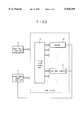
- FIG. 1 shows a block diagram of the structure of a conventional reset device.
- FIG. 2 shows a flow chart for illustrating a conventional reset operation of the conventional reset device.
- a reset signal input unit 1 inputs a reset signal to all component blocks for systematically initializing the driving mode of all the component blocks.
- the reset signal is most effective in simultaneously initialing all the component blocks.
- the component blocks include a register 2, a driving mode setting unit 3 and a port data register 4, and are driven normally or abnormally.
- step S1 if the reset signal from the reset signal input unit 1 is input to the system while any one of the component blocks is operating normally or abnormally (step S1), all the component blocks stop their operations (step S3). Then the driving mode of the overall system is initialized (step S4). If the reset signal is not input, each component block continues its present operation (step S2). In the initializing step (S4), a resetting function is performed as follows.
- the reset signal is input to discontinue the abnormal operation of the apparatus and to initialize the apparatus immediately.
- the reset signal is generated according to the user's selection. If the apparatus is operating normally, the present operation is completed and then the apparatus returns to its initial state to perform other operations.
- the above conventional reset operation automatically initializes the entire system without considering whether the operation of each component block prior to the reset signal is normal or abnormal.
- the reset signal initializes even the component blocks of the system which do not require resetting. Therefore, many component blocks of the system are unnecessarily reset to the initial state, which wastes power and operation time and results in a decreased efficiency.
- the present invention is directed to a reset device and a driving mode setting method that substantially obviates one or more of the problems due to limitations and disadvantages of the related art.
- An object of the present invention is to provide a reset device and a driving mode setting method for selectively determining whether each of the component blocks of a system need to be initialized based on the driving state of each component block prior to the reset signal, so that the user is not inconvenienced by the unnecessarily reset component blocks.
- the reset device selectively performs a reset function to maintain a present set value of a component block or to perform an initialization according to a reset signal which is selectively input to each of the component blocks according to the external or internal data provided by an apparatus having an MCU.
- the driving mode setting method using the reset device includes the steps of detecting a present state of each component block of a system when the reset signal is input, determining whether a pertinent component block need to be reset or maintained in its present driving mode, and setting the rest of the component blocks of the system based on the determination.
- the present invention is directed to a reset device for selectively resetting component blocks of a system having a microprocessor control unit, the device including reset signal means for generating a reset signal to the system; and driving means for determining whether each of the component blocks is to be initialized or maintained in its present state upon receiving the reset signal, and selectively initializing the component blocks of the system based on the determination.
- the present invention is directed to a method of selectively resetting component blocks of a system having a microprocessor control unit, the method including the steps of generating a reset signal to the system; determining whether each of the component blocks is to be initialized or maintained in its present state, upon receiving the reset signal; and selectively initializing the component blocks of the system based on the determination.
- FIG. 1 is a block diagram of a conventional reset device
- FIG. 2 is a flow chart for explaining a conventional reset operation by the conventional reset device
- FIG. 3 is a block diagram of a reset device according to one embodiment of the present invention.
- FIG. 4 is a flow chart for explaining a reset operation of the reset device according to the embodiments of the present invention.
- FIG. 5 is a block diagram of a reset device according to another embodiment of the present invention.
- FIG. 6 is a constructive illustration of a portion of a reset device according to still another embodiment of the present invention.
- all of the component blocks of a system having an MCU are not initialized by an input of a system reset signal. Instead, a reset device is utilized to determine whether each component block needs to be initialized and to initialize the component blocks according to the determination. As a result, the component blocks which do not require initialization are maintained in their present states.
- the design of the reset device may depend on the way in which the information for making such determination is received.
- the reset device as shown in FIG. 3 allows selective initializing of component blocks.
- a reset signal input unit 31 inputs a reset signal according to a user's selection when the operation of the system is in an abnormal state.
- the reset signal may be generated by the reset input unit 31 or by an external source.
- the reset signal from the input unit 31 is input to a main system having a plurality of component blocks, such as, a register 34 and a port data register 35.
- a mode setting signal input unit 32 detects the present setting of each component block in the main system and determines whether the present setting of each component block is to be maintained. Based on this determination, the mode setting signal input unit 32 inputs a mode setting signal to the main system.
- a driving mode setting unit 33 selectively initializes the component blocks based on the reset signal and the mode setting signal. That is, the register 34, the port data register 35, and other component blocks are initialized or maintained in their present states according to signals output by the driving mode setting unit 33.
- the driving mode setting unit 33 can use circuits know in the art for selectively outputting the reset signal to the component blocks based on the mode setting signal, e.g., based on the level of the mode setting signal.
- the mode setting signal input unit 32 outputs the mode setting signal to initialize the relevant component blocks according to the logic state of pins corresponding to each component block, e.g., by comparing the logic states of the pins of each component block with prestored data using a comparator known in the art.
- step S10 if the reset signal is input to the main system by the reset signal input unit 31 in step S10, the operation being performed by each component block of the main system is stopped in step S11.
- the set value of the first component block's present state is read in step S12.
- step S13 it is determined whether the present state set value of the component block is to be reused according to the information given by the mode setting signal input unit 32. If the set value of the component block is not to be reused, the set value of the component block is initialized in step S15. If the set value is to be reused, the present state of the component block is maintained in step S14.
- step S17 After completing the steps S13 to S15, if the present component block is not the last component block in the system as determined in step S16, the set value of the next component block's present state is read in step S17. The steps S13 to S17 are repeated for all of the component blocks, so that only those component blocks which need to be initialized are reset. If the reset signal is not input, the present operations of the component blocks are continuously performed in step S18.
- the component blocks which do not require initialization are unaffected by the reset signal.
- the present state set values are reused in a manner similar to a restart operation.
- a reset device and a driving mode setting method according to another embodiment of the present invention are as follows.
- the reset device includes a register block for deciding whether the present state set value of each component block is to be reused. If there is an insufficient number of ports in the system, a separate register is used to determine the present state set value of each component block. Once the register block or separate register determines that the set value of the component block is to be reused, initialization of that component block does not occur even if the reset signal is received.
- the reset device includes a reset signal input unit 131 for inputting a reset signal according to the user's selection when the operation of the apparatus having the MCU is abnormal, a decision register circuit 136 (register block) for receiving the reset signal, and a plurality of component blocks.
- the decision register circuit 136 includes a register, e.g., for storing data therein.
- the reset signal can be generated by the reset signal input unit 131 or by an external source.
- the component blocks include a register 134, a port data register 135, and a driving mode setting unit 133.
- the decision register circuit 136 detects the set value of the present state of each component block in the main system and determines if the set value can be reused, e.g., by comparing the detected values of the present state of each component block with prestored data using a comparator known in the art. Based on this determination, the decision register circuit 136 selectively initializes only the component blocks which need to be initialized. The states of other component blocks are maintained.
- the driving mode setting method utilizes the reset device as shown in FIG. 5.
- This method is substantially the same as the method described referring to FIG. 4, except that the reset signal input by the reset signal input unit 131 passes through the decision register circuit 136 before it reaches the appropriate component blocks.
- the decision register circuit 136 stores data for determining whether or not the present state set value of each component block is reusable. Therefore, the decision register circuit 136 selectively transmits the reset signal to the component blocks based on this data.
- a reset device and a driving mode setting Method according to still another embodiment of the present invention is described as follows.
- FIG. 6 shows a plurality of registers each corresponding to a component block of the main system. Each register stores information relevant to authorize initialization of the corresponding component block.
- a register of each component block of the main system is provided with a decision bit.
- the decision bit may be stored in an unused space of the register or in a newly added memory.
- the decision bit indicates whether the corresponding block component is to be initialized or to be maintained in its present state. For example, the "0" decision bit may allow initialization of the component block, whereas the "1" decision bit may cause the component block to be maintained in its present state.
- each component block When the reset signal by a reset signal input unit is directly input to each of the component blocks of the main system, each component block is reset or maintained in its present set value, depending on the value of the decision bit (0 or 1) stored in the corresponding register.
- the driving mode setting method using the above reset device operates in the same manner as the method described referring to FIG. 4, except that each component block stores the information necessary to decide whether the component block is to be initialized. Therefore, reading of the component block's present state set value for determining whether the component block is to be initialized, is substituted by reading the decision bit stored in the register of the component block. Based on the value of the decision bit, the component block is initialized or maintained in its present state.
- not all of the component blocks are initialized even if the reset signal is input.
- Some set values of the component blocks are selectively kept so that the component blocks which do not require initialization can perform their previous operations without interruptions. Consequently, there is no need to have an initial program for specifying the states of the component blocks. As a result, a smaller memory size can be used.
- the present invention facilitates error detection, thereby facilitating programming and increasing system efficiency.
Landscapes
- Engineering & Computer Science (AREA)
- Theoretical Computer Science (AREA)
- Physics & Mathematics (AREA)
- General Engineering & Computer Science (AREA)
- General Physics & Mathematics (AREA)
- Microcomputers (AREA)
- Debugging And Monitoring (AREA)
- Electronic Switches (AREA)
- Retry When Errors Occur (AREA)
Abstract
Description
Claims (20)
Applications Claiming Priority (2)
| Application Number | Priority Date | Filing Date | Title |
|---|---|---|---|
| KR1019960049054A KR100209762B1 (en) | 1996-10-28 | 1996-10-28 | Reset apparatus and operation mode regulating method using its |
| KR96-49054 | 1996-10-28 |
Publications (1)
| Publication Number | Publication Date |
|---|---|
| US5928359A true US5928359A (en) | 1999-07-27 |
Family
ID=19479235
Family Applications (1)
| Application Number | Title | Priority Date | Filing Date |
|---|---|---|---|
| US08/866,237 Expired - Lifetime US5928359A (en) | 1996-10-28 | 1997-05-30 | Device and method for selectively resetting component blocks of a system |
Country Status (3)
| Country | Link |
|---|---|
| US (1) | US5928359A (en) |
| JP (1) | JPH10143285A (en) |
| KR (1) | KR100209762B1 (en) |
Cited By (5)
| Publication number | Priority date | Publication date | Assignee | Title |
|---|---|---|---|---|
| US6446201B1 (en) * | 1998-09-17 | 2002-09-03 | Hartmann & Braun Gmbh & Co. Kg | Method and system of sending reset signals only to slaves requiring reinitialization by a bus master |
| US20020161992A1 (en) * | 2001-04-26 | 2002-10-31 | Fujitsu Limited | Processor and reset control method for the processor |
| US6792527B1 (en) * | 2000-12-22 | 2004-09-14 | Xilinx, Inc. | Method to provide hierarchical reset capabilities for a configurable system on a chip |
| US20070168688A1 (en) * | 2005-10-04 | 2007-07-19 | Chelstrom Nathan P | Clock control hierarchy for integrated microprocessors and systems-on-a-chip |
| US20080091863A1 (en) * | 2006-10-16 | 2008-04-17 | Samsung Electronics Co., Ltd. | Apparatus and method for generating reset signals for function chips in a terminal |
Families Citing this family (4)
| Publication number | Priority date | Publication date | Assignee | Title |
|---|---|---|---|---|
| KR100476870B1 (en) * | 1997-09-24 | 2005-07-05 | 삼성전자주식회사 | Initializing signal generating circuit for control register |
| DE102007034692A1 (en) * | 2006-07-12 | 2008-02-14 | Samsung Electronics Co., Ltd., Suwon | Memory card e.g. smart card, resetting method for e.g. mobile phone, involves resetting set of function blocks when no interface other than selected interface is active, and detecting interface related to reset signal |
| KR100764743B1 (en) | 2006-07-12 | 2007-10-08 | 삼성전자주식회사 | Memory card including reset control unit and reset control method thereof |
| JP5258610B2 (en) * | 2009-02-10 | 2013-08-07 | 三菱電機株式会社 | Electrical circuit and standby system |
Citations (4)
| Publication number | Priority date | Publication date | Assignee | Title |
|---|---|---|---|---|
| US5086505A (en) * | 1989-06-30 | 1992-02-04 | Motorola, Inc. | Selective individual reset apparatus and method |
| US5155856A (en) * | 1988-08-27 | 1992-10-13 | International Business Machines Corporation | Arrangement in a self-guarding data processing system for system initialization and reset |
| US5465360A (en) * | 1989-11-03 | 1995-11-07 | Compaq Computer Corp. | Method and apparatus for independently resetting processors and cache controllers in multiple processor systems |
| US5758185A (en) * | 1992-10-01 | 1998-05-26 | Hudson Soft Co. Ltd. | Method for resetting a system controlled by a CPU and having a semi-autonomous IC unit |
-
1996
- 1996-10-28 KR KR1019960049054A patent/KR100209762B1/en not_active IP Right Cessation
-
1997
- 1997-05-30 US US08/866,237 patent/US5928359A/en not_active Expired - Lifetime
- 1997-09-04 JP JP9239384A patent/JPH10143285A/en active Pending
Patent Citations (4)
| Publication number | Priority date | Publication date | Assignee | Title |
|---|---|---|---|---|
| US5155856A (en) * | 1988-08-27 | 1992-10-13 | International Business Machines Corporation | Arrangement in a self-guarding data processing system for system initialization and reset |
| US5086505A (en) * | 1989-06-30 | 1992-02-04 | Motorola, Inc. | Selective individual reset apparatus and method |
| US5465360A (en) * | 1989-11-03 | 1995-11-07 | Compaq Computer Corp. | Method and apparatus for independently resetting processors and cache controllers in multiple processor systems |
| US5758185A (en) * | 1992-10-01 | 1998-05-26 | Hudson Soft Co. Ltd. | Method for resetting a system controlled by a CPU and having a semi-autonomous IC unit |
Non-Patent Citations (2)
| Title |
|---|
| Mitsubishi Co. Data Book: '94 Data Book, "Something New", p. 11, pp. 77-80. |
| Mitsubishi Co. Data Book: 94 Data Book, Something New , p. 11, pp. 77 80. * |
Cited By (8)
| Publication number | Priority date | Publication date | Assignee | Title |
|---|---|---|---|---|
| US6446201B1 (en) * | 1998-09-17 | 2002-09-03 | Hartmann & Braun Gmbh & Co. Kg | Method and system of sending reset signals only to slaves requiring reinitialization by a bus master |
| US6792527B1 (en) * | 2000-12-22 | 2004-09-14 | Xilinx, Inc. | Method to provide hierarchical reset capabilities for a configurable system on a chip |
| US20020161992A1 (en) * | 2001-04-26 | 2002-10-31 | Fujitsu Limited | Processor and reset control method for the processor |
| US6963969B2 (en) * | 2001-04-26 | 2005-11-08 | Fujitsu Limited | Method and processor for initializing a plurality of non-overlapping areas with associated flags and signals |
| US20070168688A1 (en) * | 2005-10-04 | 2007-07-19 | Chelstrom Nathan P | Clock control hierarchy for integrated microprocessors and systems-on-a-chip |
| US7627771B2 (en) * | 2005-10-04 | 2009-12-01 | International Business Machines Corporation | Clock control hierarchy for integrated microprocessors and systems-on-a-chip |
| US20080091863A1 (en) * | 2006-10-16 | 2008-04-17 | Samsung Electronics Co., Ltd. | Apparatus and method for generating reset signals for function chips in a terminal |
| US7814305B2 (en) * | 2006-10-16 | 2010-10-12 | Samsung Electronics Co., Ltd | Apparatus and method for generating reset signals for function chips in a terminal |
Also Published As
| Publication number | Publication date |
|---|---|
| KR100209762B1 (en) | 1999-07-15 |
| KR19980029728A (en) | 1998-07-25 |
| JPH10143285A (en) | 1998-05-29 |
Similar Documents
| Publication | Publication Date | Title |
|---|---|---|
| CA2046356C (en) | Method and apparatus for improved initialization of computer system features | |
| EP0127440A2 (en) | Integrated circuit device incorporating a data processing unit and a ROM storing applications program therein | |
| EP0469239A2 (en) | Small programmable array associated to the on-chip control store for microcode correction | |
| US5928359A (en) | Device and method for selectively resetting component blocks of a system | |
| JPH08137763A (en) | Flash memory controller | |
| US7093115B2 (en) | Method and apparatus for detecting an interruption in memory initialization | |
| US6571347B1 (en) | Apparatus and method for intelligent computer initiation program recovery | |
| KR100238917B1 (en) | Supervision of microprocessors | |
| US20090193242A1 (en) | Computer system with dual basic input output system and operation method thereof | |
| US7596681B2 (en) | Processor and processing method for reusing arbitrary sections of program code | |
| US5958074A (en) | Data processor having data bus and instruction fetch bus provided separately from each other | |
| KR100377608B1 (en) | Data processor and method of processing data | |
| WO1980002881A1 (en) | Microcomputer with mpu-programmable eprom | |
| JP3091526B2 (en) | Processing element and method of programming such a processing element | |
| JP2003167649A (en) | Information processor | |
| JP2007157143A (en) | Processing arrangement, memory card device and method for operating and manufacturing processing arrangement | |
| EP0381140A2 (en) | Data processing apparatus | |
| KR100290280B1 (en) | Microcontroller with Programmable Flash Memory | |
| US6378034B1 (en) | Microcomputer with flash EEPROM having automatic communication mode determining function | |
| JPH0527875A (en) | Electronic equipment | |
| KR960003096B1 (en) | Error detecting circuit | |
| KR20020067144A (en) | Apparatus and method for reset confirmation of computer system | |
| KR20070037922A (en) | Image display apparatus controlling communication of inside circuit-module and method thereof | |
| JPH1196012A (en) | Distributed controller | |
| JPH0764822A (en) | Microcomputer |
Legal Events
| Date | Code | Title | Description |
|---|---|---|---|
| AS | Assignment |
Owner name: LG SEMICON CO., LTD., KOREA, REPUBLIC OF Free format text: ASSIGNMENT OF ASSIGNORS INTEREST;ASSIGNOR:LEE, KANG BOK;REEL/FRAME:008593/0562 Effective date: 19970512 |
|
| STCF | Information on status: patent grant |
Free format text: PATENTED CASE |
|
| FEPP | Fee payment procedure |
Free format text: PAYOR NUMBER ASSIGNED (ORIGINAL EVENT CODE: ASPN); ENTITY STATUS OF PATENT OWNER: LARGE ENTITY |
|
| FPAY | Fee payment |
Year of fee payment: 4 |
|
| AS | Assignment |
Owner name: HYNIX SEMICONDUCTOR INC., KOREA, REPUBLIC OF Free format text: CHANGE OF NAME;ASSIGNOR:LG SEMICON CO., LTD.;REEL/FRAME:015246/0634 Effective date: 19990726 |
|
| AS | Assignment |
Owner name: MAGNACHIP SEMICONDUCTOR, LTD., KOREA, REPUBLIC OF Free format text: ASSIGNMENT OF ASSIGNORS INTEREST;ASSIGNOR:HYNIX SEMICONDUCTOR, INC.;REEL/FRAME:016216/0649 Effective date: 20041004 |
|
| AS | Assignment |
Owner name: U.S. BANK NATIONAL ASSOCIATION, AS COLLATERAL TRUS Free format text: SECURITY INTEREST;ASSIGNOR:MAGNACHIP SEMICONDUCTOR, LTD.;REEL/FRAME:016470/0530 Effective date: 20041223 |
|
| FPAY | Fee payment |
Year of fee payment: 8 |
|
| FEPP | Fee payment procedure |
Free format text: PAYER NUMBER DE-ASSIGNED (ORIGINAL EVENT CODE: RMPN); ENTITY STATUS OF PATENT OWNER: LARGE ENTITY |
|
| FEPP | Fee payment procedure |
Free format text: PAYOR NUMBER ASSIGNED (ORIGINAL EVENT CODE: ASPN); ENTITY STATUS OF PATENT OWNER: LARGE ENTITY |
|
| AS | Assignment |
Owner name: MAGNACHIP SEMICONDUCTOR LTD.,KOREA, DEMOCRATIC PEO Free format text: RELEASE BY SECURED PARTY;ASSIGNOR:U.S. BANK NATIONAL ASSOCIATION;REEL/FRAME:024563/0807 Effective date: 20100527 |
|
| FPAY | Fee payment |
Year of fee payment: 12 |
|
| AS | Assignment |
Owner name: MAGNACHIP SEMICONDUCTOR LTD., KOREA, REPUBLIC OF Free format text: CORRECTIVE ASSIGNMENT TO CORRECT THE RECEIVING PARTY ADDRESS PREVIOUSLY RECORDED AT REEL: 024563 FRAME: 0807. ASSIGNOR(S) HEREBY CONFIRMS THE RELEASE BY SECURED PARTY;ASSIGNOR:US BANK NATIONAL ASSOCIATION;REEL/FRAME:034469/0001 Effective date: 20100527 |