US5889301A - Semiconductor memory device having an E-shaped storage node - Google Patents
Semiconductor memory device having an E-shaped storage node Download PDFInfo
- Publication number
- US5889301A US5889301A US08/725,807 US72580796A US5889301A US 5889301 A US5889301 A US 5889301A US 72580796 A US72580796 A US 72580796A US 5889301 A US5889301 A US 5889301A
- Authority
- US
- United States
- Prior art keywords
- layer
- capacitor
- storage node
- insulating layer
- polysilicon
- Prior art date
- Legal status (The legal status is an assumption and is not a legal conclusion. Google has not performed a legal analysis and makes no representation as to the accuracy of the status listed.)
- Expired - Lifetime
Links
Images


Classifications
-
- H—ELECTRICITY
- H10—SEMICONDUCTOR DEVICES; ELECTRIC SOLID-STATE DEVICES NOT OTHERWISE PROVIDED FOR
- H10B—ELECTRONIC MEMORY DEVICES
- H10B12/00—Dynamic random access memory [DRAM] devices
- H10B12/30—DRAM devices comprising one-transistor - one-capacitor [1T-1C] memory cells
- H10B12/31—DRAM devices comprising one-transistor - one-capacitor [1T-1C] memory cells having a storage electrode stacked over the transistor
- H10B12/318—DRAM devices comprising one-transistor - one-capacitor [1T-1C] memory cells having a storage electrode stacked over the transistor the storage electrode having multiple segments
-
- H—ELECTRICITY
- H10—SEMICONDUCTOR DEVICES; ELECTRIC SOLID-STATE DEVICES NOT OTHERWISE PROVIDED FOR
- H10B—ELECTRONIC MEMORY DEVICES
- H10B12/00—Dynamic random access memory [DRAM] devices
- H10B12/01—Manufacture or treatment
- H10B12/02—Manufacture or treatment for one transistor one-capacitor [1T-1C] memory cells
- H10B12/03—Making the capacitor or connections thereto
- H10B12/033—Making the capacitor or connections thereto the capacitor extending over the transistor
Definitions
- the present invention relates to a method of fabricating a dynamic random access memory having an increased capacitance capacitor having an E-shaped storage node.
- DRAMs In recent years there has been a dramatic increase in the packing density of DRAMs. Large DRAM devices are normally silicon based, and each cell typically embodies a single MOS field effect transistor with its source connected to a storage capacitor. This large integration of DRAMs has been accomplished by a reduction in individual cell size. However, the reduction in cell size results in a decrease in storage capacitance leading to reliability drawbacks, such as a lowering of source/drain ratio and undesirable signal problems. In order to achieve the desired higher level of integration, the technology must keep almost the same storage capacitance on a greatly reduced cell area.
- a method for forming a dynamic random access memory cell with an increased capacitance capacitor Relatively thick field oxide areas are formed on the surface of a semiconductor substrate while leaving device areas for fabrication of semiconductor devices.
- Device structures are formed within the device areas of the semiconductor substrate wherein the device structures include a capacitor node contact region within the silicon substrate.
- the capacitors are formed by the following steps.
- a dielectric layer is deposited overlying the semiconductor device structures.
- An insulating layer is deposited overlying the dielectric layer and is planarized.
- a contact is opened through the insulating layer and the dielectric layer to the capacitor node contact region.
- a first layer of polysilicon is deposited overlying the insulating layer and filling the contact opening wherein the portion of the first polysilicon layer contacting the node contact region forms the bottom electrode of the capacitor.
- a portion of the first polysilicon layer is etched away wherein a well opening is formed above the contact opening.
- a layer of silicon oxide is deposited overlying the first polysilicon layer and conformally within the well opening. The silicon oxide layer is etched back to leave spacers on the sidewalls of the well opening.
- a second layer of polysilicon is deposited overlying the first polysilicon layer and within the well opening. The second polysilicon layer is removed except where the second polysilicon layer forms a plug within the well opening.
- the spacers on the walls of the well opening are removed wherein gaps are left on either side of the plug.
- the first polysilicon layer is patterned so that an E-shaped structure having three prongs is formed wherein the prongs of the E-shaped structure point upward and wherein the plug forms the central prong and wherein the outer two prongs are formed by the patterned first polysilicon layer and wherein the E-shaped structure forms the storage node of the capacitor.
- a capacitor dielectric layer is deposited over all surfaces of the substrate wherein the capacitor dielectric layer covers the surfaces of the E-shaped structure.
- a third polysilicon layer is deposited overlying the capacitor dielectric layer wherein the third polysilicon layer covers and fills the gaps of the E-shaped structure and wherein the third polysilicon layer forms the top electrode of the capacitor to complete formation of the DRAM with capacitor.
- a dynamic random access memory having a high capacitance capacitor is described.
- Field oxide areas on the surface of a semiconductor substrate surround device areas for fabrication of field effect devices, gate dielectric and electrode structures on the substrate in the device areas.
- Source/drain structures associated with the gate structures lie within the device areas of the semiconductor substrate.
- a capacitor structure comprises a bottom electrode formed by the central cylindrical portion of a polysilicon layer which electrically contacts the source/drain structures, a storage node having an E-shape with three prongs wherein the prongs point upward from the central cylindrical portion of the polysilicon layer, a capacitor dielectric layer overlying all surfaces of the storage node, and a top plate electrode layer overlying the capacitor dielectric layer on all surfaces of the storage node to complete the capacitor.
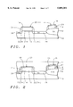
- FIGS. 1 through 12 are schematic cross-sectional representations of a preferred embodiment of the present invention.
- FIGS. 9A and 9B schematically illustrate in cross-sectional representation two alternative methods in the process of the present invention.
- the first series of steps involve the formation of the dielectric isolation regions for isolating semiconductor surface regions from other such regions in the semiconductor substrate 10.
- the semiconductor substrate is preferably composed of silicon having a (100) crystallographic orientation.
- Field oxide regions 12 are formed in and on the semiconductor substrate.
- the surface of the silicon substrate 10 is thermally oxidized to form the desired gate oxide 14 thickness.
- the preferred thickness is between about 80 to 200 Angstroms.
- the polysilicon layer 16 is blanket deposited by low pressure chemical vapor deposition (LPCVD) to a preferred thickness of between about 1500 to 3500 Angstroms.
- a layer 18 of silicon oxide is chemically vapor deposited over the surface of the polysilicon to a thickness of between about 600 to 1200 Angstroms.
- the layers 14, 16, and 18 are patterned by lithography and anisotropic etching techniques as are conventional in the art to provide a desired pattern of gate electrodes and word lines 20 as seen in FIG. 1.
- FIGS. 1 through 12 illustrate the formation of an N channel FET integrated circuit device.
- a P channel FET integrated circuit device could also be formed by simply substituting opposite polarities to those given for the N channel embodiment.
- a CMOS FET could in a similar way be formed by making both N channel and P channel devices upon the same substrate.
- the DRAM cell is composed of a combination device structure of an N channel FET and a stacked capacitor while the peripheral circuits are often composed of CMOS devices.
- FIG. 1 shows the ion implantations of N- dopants.
- Lithographic masks may be required to protect the areas not to be subjected to that particular N- ion implantation.
- the formation of the lithographic masks is done by conventional lithography and etching techniques.
- the N- lightly doped drain implantation 22 is done with, for example, P 31 at a dosage of between about 1 E 13 to 1 E 14 atoms/cm 2 and an energy of between about 20 to 40 Kev.
- the dielectric spacer 24 is now to be formed followed by the completion of the lightly doped drain source/drain structures.
- a tetraethyloxysilane (TEOS) LPCVD deposition is preferred to a thickness of between about 1000 to 2000 Angstroms.
- the heavily doped source and drain regions 26 are formed by implantation with, for example, arsenic at a dosage of between about 1 E 15 to 1 E 16 atoms/cm 2 and an energy of between about 20 to 80 Kev.
- a layer of silicon oxide or nitride 28 is formed over the field oxide and device areas to a thickness of between about 800 to 2000 Angstroms.
- a thick insulating layer such as chemically vapor deposited (CVD) oxide or borophosphosilicate glass (BPSG) 30 is deposited to a thickness of between about 5000 to 10,000 Angstroms and then planarized, for example by chemical mechanical polishing (CMP), to obtain a flat surface.
- CVD chemically vapor deposited
- BPSG borophosphosilicate glass
- contact openings are made through the CVD oxide or BPSG layer 30 and silicon nitride layer 28 to the silicon substrate. Opening 31 is made to the node contact region for the capacitor structure.
- a first thick polysilicon layer 32 is deposited over CVD oxide or BPSG layer 30 by LPCVD either in situ doped or doped after deposition by ion implantation.
- the thickness of this layer is between about 2000 to 6000 Angstroms.
- the thick polysilicon layer 32 is anisotropically etched into to form a well 34, as shown in FIG. 5. This may be a Magnetic Enhanced Reactive Ion Etching (MERIE).
- MERIE Magnetic Enhanced Reactive Ion Etching
- the width of the well 34 can be of the minimum dimension on the chip.
- the depth of the well 34 must be less than the thickness of layer 32.
- a layer of silicon oxide 36 is deposited over layer 32 and within the well 34 by CVD to a thickness of between about 2000 to 6000 Angstroms, as illustrated in FIG. 6.
- the silicon oxide layer 36 is etched back, using MERIE, to form spacers on the sidewalls of the well 34.
- a second layer of polysilicon 38 is deposited over the first polysilicon layer 32, spacers 36, and within the well 34.
- the in-situ doped polysilicon layer 38 is deposited by LPCVD. This layer has a thickness of between about 500 to 1500 Angstroms.
- the polysilicon layer 38 is thermally oxidized to form polyoxide layer 40, shown in FIG. 9A.
- the polyoxide layer 40 and oxide spacers 36 are removed, using, for example, a hydrofluoric acid solution, to leave polysilicon plug 42.
- the polysilicon layer 38 can be etched back to leave the polysilicon plug 42, as shown in FIG. 9B. Then the oxide spacers 36 can be removed using, for example, a hydrofluoric acid solution, resulting also in FIG. 10.
- the polysilicon layer 32 is patterned to form the storage node of the capacitor.
- the portion of layer 32 contacting the node contact region forms the bottom electrode of the capacitor.
- Layer 32 and plug 42 together form the E-shaped storage node of the capacitor where the three prongs of the E-shape point upward.
- the capacitor dielectric layer 44 is now deposited conformally over the polysilicon 32 and 42 and insulating layer 30 surfaces.
- This layer is typically either composed of layers of silicon nitride and silicon oxide (NO) or layers of silicon oxide, silicon nitride and silicon oxide (ONO).
- the first or bottom silicon oxide, O layer is usually a native oxide grown to a thickness of about 15 Angstroms.
- the silicon nitride, N layer is formed by LPCVD to give a resulting thickness of between about 80 to 200 Angstroms.
- the top silicon oxide, O layer may be formed in an oxidation furnace.
- the total ONO thickness is in the order of between about 100 to 250 Angstroms.
- the top plate electrode is formed by depositing a third in-situ doped polysilicon layer 46 by LPCVD.
- the thickness of this layer 46 is between about 1000 to 2000 Angstroms.
- the process of the invention results in an increased capacitance DRAM capacitor having an E-shaped storage node. Since the insulating layer 30 is planarized using CMP, the etchback to form the plug 42, which forms the middle prong of the E-shape, leaves no residue.
- MOS devices such as gate electrodes and word lines 20 lie on a semiconductor substrate 10.
- Source and drain regions 26 lie within the semiconductor substrate not covered by the MOS devices.
- a stacked capacitor 32 contacts one of the source and drain regions 26.
- the storage node of the capacitor comprises a cylindrical polysilicon structure 32 at the top of which is an E-shaped polysilicon structure 32,42 having the prongs of the E pointing upward.
- the capacitor dielectric 44 comprises NO or ONO covering all surfaces of the storage node 32 and 42.
- the top electrode 46 comprises polysilicon overlying the capacitor dielectric.
Abstract
Description
Claims (6)
Priority Applications (1)
| Application Number | Priority Date | Filing Date | Title |
|---|---|---|---|
| US08/725,807 US5889301A (en) | 1996-06-10 | 1996-10-04 | Semiconductor memory device having an E-shaped storage node |
Applications Claiming Priority (2)
| Application Number | Priority Date | Filing Date | Title |
|---|---|---|---|
| US08/661,245 US5604146A (en) | 1996-06-10 | 1996-06-10 | Method to fabricate a semiconductor memory device having an E-shaped storage node |
| US08/725,807 US5889301A (en) | 1996-06-10 | 1996-10-04 | Semiconductor memory device having an E-shaped storage node |
Related Parent Applications (1)
| Application Number | Title | Priority Date | Filing Date |
|---|---|---|---|
| US08/661,245 Division US5604146A (en) | 1996-06-10 | 1996-06-10 | Method to fabricate a semiconductor memory device having an E-shaped storage node |
Publications (1)
| Publication Number | Publication Date |
|---|---|
| US5889301A true US5889301A (en) | 1999-03-30 |
Family
ID=24652789
Family Applications (2)
| Application Number | Title | Priority Date | Filing Date |
|---|---|---|---|
| US08/661,245 Expired - Lifetime US5604146A (en) | 1996-06-10 | 1996-06-10 | Method to fabricate a semiconductor memory device having an E-shaped storage node |
| US08/725,807 Expired - Lifetime US5889301A (en) | 1996-06-10 | 1996-10-04 | Semiconductor memory device having an E-shaped storage node |
Family Applications Before (1)
| Application Number | Title | Priority Date | Filing Date |
|---|---|---|---|
| US08/661,245 Expired - Lifetime US5604146A (en) | 1996-06-10 | 1996-06-10 | Method to fabricate a semiconductor memory device having an E-shaped storage node |
Country Status (1)
| Country | Link |
|---|---|
| US (2) | US5604146A (en) |
Cited By (7)
| Publication number | Priority date | Publication date | Assignee | Title |
|---|---|---|---|---|
| US6064085A (en) * | 1998-06-03 | 2000-05-16 | Texas Instruments-Acer Incorporated | DRAM cell with a multiple fin-shaped structure capacitor |
| US6097055A (en) * | 1998-04-18 | 2000-08-01 | Samsung Electronics Co., Ltd. | Capacitor and method for fabricating the same |
| US6350707B1 (en) * | 1999-09-03 | 2002-02-26 | United Microelectronics Corp. | Method of fabricating capacitor dielectric |
| US6424043B1 (en) | 1997-03-13 | 2002-07-23 | Micron Technology, Inc. | Semiconductor processing methods of forming integrated circuitry memory devices, methods of forming capacitor containers, methods of making electrical connection to circuit nodes and related integrated circuitry |
| KR100422063B1 (en) * | 2001-05-02 | 2004-03-10 | 삼성전자주식회사 | Capacitor in semiconductor device and method for manufacturing the same |
| US6707096B2 (en) * | 1996-12-05 | 2004-03-16 | Micron Technology, Inc. | Fork-like memory structure for ULSI DRAM and method of fabrication |
| US20060022260A1 (en) * | 2004-07-29 | 2006-02-02 | Renesas Technology Corp. | Semiconductor device and manufacturing method of semiconductor device |
Families Citing this family (22)
| Publication number | Priority date | Publication date | Assignee | Title |
|---|---|---|---|---|
| JP3156878B2 (en) * | 1992-04-30 | 2001-04-16 | 株式会社東芝 | Semiconductor device and method of manufacturing the same |
| US5753559A (en) * | 1996-01-16 | 1998-05-19 | United Microelectronics Corporation | Method for growing hemispherical grain silicon |
| JPH1022476A (en) * | 1996-07-02 | 1998-01-23 | Sony Corp | Capacitive element |
| US5766993A (en) * | 1996-11-25 | 1998-06-16 | Vanguard International Semiconductor Corporation | Method of fabricating storage node electrode, for DRAM devices, using polymer spacers, to obtain polysilicon columns, with minimum spacing between columns |
| GB2322964B (en) * | 1997-03-07 | 2001-10-17 | United Microelectronics Corp | Polysilicon CMP process for high-density DRAM cell structures |
| US6322600B1 (en) | 1997-04-23 | 2001-11-27 | Advanced Technology Materials, Inc. | Planarization compositions and methods for removing interlayer dielectric films |
| US5899716A (en) * | 1997-05-19 | 1999-05-04 | Vanguard International Semiconductor Corporation | Oxygen ion implantation procedure to increase the surface area of an STC structure |
| US5770499A (en) * | 1997-05-29 | 1998-06-23 | Texas Instruments Incorporated | Planarized capacitor array structure for high density memory applications |
| TW330326B (en) * | 1997-07-18 | 1998-04-21 | Nanya Technology Co Ltd | The manufacturing method for semiconductor capacitor electrode plate |
| US5920763A (en) * | 1997-08-21 | 1999-07-06 | Micron Technology, Inc. | Method and apparatus for improving the structural integrity of stacked capacitors |
| US5926710A (en) * | 1997-10-23 | 1999-07-20 | Vanguard International Semiconductor Corporation | Method for making dynamic random access memory cells using a novel stacked capacitor process |
| US5940701A (en) * | 1997-12-03 | 1999-08-17 | Vanguard International Semiconductor Corporation | Method for forming a DRAM capacitor with four polysilicon pillars |
| US5956587A (en) * | 1998-02-17 | 1999-09-21 | Vanguard International Semiconductor Corporation | Method for crown type capacitor in dynamic random access memory |
| US5895250A (en) * | 1998-06-11 | 1999-04-20 | Vanguard International Semiconductor Corporation | Method of forming semicrown-shaped stacked capacitors for dynamic random access memory |
| US6063548A (en) * | 1998-09-04 | 2000-05-16 | Taiwan Semiconductor Manufacturing Company | Method for making DRAM using a single photoresist masking step for making capacitors with node contacts |
| US6071773A (en) * | 1998-10-05 | 2000-06-06 | Taiwan Semiconductor Manufacturing Company | Process for fabricating a DRAM metal capacitor structure for use in an integrated circuit |
| US6165865A (en) * | 1998-10-30 | 2000-12-26 | United Microelectronics Corp. | Method of fabricating dual cylindrical capacitor |
| US6033966A (en) * | 1998-11-09 | 2000-03-07 | Worldwide Seminconductor Manufacturing Corporation | Method for making an 8-shaped storage node DRAM cell |
| US6130127A (en) * | 1999-07-23 | 2000-10-10 | Vanguard International Semiconductor Corporation | Method for making dynamic random access memory cells having cactus-shaped stacked capacitors with increased capacitance |
| US6686235B2 (en) * | 2001-04-12 | 2004-02-03 | Micron Technology, Inc. | Buried digit spacer-separated capacitor array |
| US6815753B2 (en) * | 2002-08-29 | 2004-11-09 | Micron Technology, Inc. | Semiconductor capacitor structure and method to form same |
| TWI310214B (en) * | 2006-06-07 | 2009-05-21 | Promos Technologies Inc | A capacitor structure of a semiconducotr memory and a method for preparing the same |
Citations (14)
| Publication number | Priority date | Publication date | Assignee | Title |
|---|---|---|---|---|
| US5126280A (en) * | 1991-02-08 | 1992-06-30 | Micron Technology, Inc. | Stacked multi-poly spacers with double cell plate capacitor |
| US5150276A (en) * | 1992-01-24 | 1992-09-22 | Micron Technology, Inc. | Method of fabricating a vertical parallel cell capacitor having a storage node capacitor plate comprising a center fin effecting electrical communication between itself and parallel annular rings |
| US5158905A (en) * | 1990-11-29 | 1992-10-27 | Samsung Electronics Corp., Ltd. | Method for manufacturing a semiconductor device with villus-type capacitor |
| US5164881A (en) * | 1991-01-30 | 1992-11-17 | Samsung Electronics Co., Ltd. | Highly integrated semiconductor memory device and the fabrication method thereof |
| US5223729A (en) * | 1990-09-26 | 1993-06-29 | Matsushita Electric Industrial Co., Ltd. | Semiconductor device and a method of producing the same |
| US5274258A (en) * | 1991-01-30 | 1993-12-28 | Samsung Electronics Co., Ltd. | High density semiconductor memory device (MBC cell) |
| US5285092A (en) * | 1988-12-08 | 1994-02-08 | Mitsubishi Denki Kabushiki Kaisha | Semiconductor memory device having a stacked type capacitor and manufacturing method therefor |
| US5338700A (en) * | 1993-04-14 | 1994-08-16 | Micron Semiconductor, Inc. | Method of forming a bit line over capacitor array of memory cells |
| US5364809A (en) * | 1991-05-23 | 1994-11-15 | Samsung Electronics Co., Ltd. | Method of fabricating a capacitor for a dynamic random access memory cell |
| US5389568A (en) * | 1992-10-29 | 1995-02-14 | Samsung Electronics Co., Ltd. | Method of making a dynamic random access memory device |
| US5438013A (en) * | 1992-08-26 | 1995-08-01 | Samsung Electronics Co., Ltd. | Method of making a semiconductor memory device having a capacitor |
| US5512768A (en) * | 1994-03-18 | 1996-04-30 | United Microelectronics Corporation | Capacitor for use in DRAM cell using surface oxidized silicon nodules |
| US5572053A (en) * | 1987-11-25 | 1996-11-05 | Fujitsu Limited | Dynamic random access memory cell having a stacked capacitor |
| US5714779A (en) * | 1992-06-30 | 1998-02-03 | Siemens Aktiengesellschaft | Semiconductor memory device having a transistor, a bit line, a word line and a stacked capacitor |
Family Cites Families (3)
| Publication number | Priority date | Publication date | Assignee | Title |
|---|---|---|---|---|
| US5340763A (en) * | 1993-02-12 | 1994-08-23 | Micron Semiconductor, Inc. | Multi-pin stacked capacitor utilizing micro villus patterning in a container cell and method to fabricate same |
| US5354705A (en) * | 1993-09-15 | 1994-10-11 | Micron Semiconductor, Inc. | Technique to fabricate a container structure with rough inner and outer surfaces |
| US5418180A (en) * | 1994-06-14 | 1995-05-23 | Micron Semiconductor, Inc. | Process for fabricating storage capacitor structures using CVD tin on hemispherical grain silicon |
-
1996
- 1996-06-10 US US08/661,245 patent/US5604146A/en not_active Expired - Lifetime
- 1996-10-04 US US08/725,807 patent/US5889301A/en not_active Expired - Lifetime
Patent Citations (15)
| Publication number | Priority date | Publication date | Assignee | Title |
|---|---|---|---|---|
| US5572053A (en) * | 1987-11-25 | 1996-11-05 | Fujitsu Limited | Dynamic random access memory cell having a stacked capacitor |
| US5285092A (en) * | 1988-12-08 | 1994-02-08 | Mitsubishi Denki Kabushiki Kaisha | Semiconductor memory device having a stacked type capacitor and manufacturing method therefor |
| US5223729A (en) * | 1990-09-26 | 1993-06-29 | Matsushita Electric Industrial Co., Ltd. | Semiconductor device and a method of producing the same |
| US5158905A (en) * | 1990-11-29 | 1992-10-27 | Samsung Electronics Corp., Ltd. | Method for manufacturing a semiconductor device with villus-type capacitor |
| US5164881A (en) * | 1991-01-30 | 1992-11-17 | Samsung Electronics Co., Ltd. | Highly integrated semiconductor memory device and the fabrication method thereof |
| US5274258A (en) * | 1991-01-30 | 1993-12-28 | Samsung Electronics Co., Ltd. | High density semiconductor memory device (MBC cell) |
| US5126280A (en) * | 1991-02-08 | 1992-06-30 | Micron Technology, Inc. | Stacked multi-poly spacers with double cell plate capacitor |
| US5364809A (en) * | 1991-05-23 | 1994-11-15 | Samsung Electronics Co., Ltd. | Method of fabricating a capacitor for a dynamic random access memory cell |
| US5150276A (en) * | 1992-01-24 | 1992-09-22 | Micron Technology, Inc. | Method of fabricating a vertical parallel cell capacitor having a storage node capacitor plate comprising a center fin effecting electrical communication between itself and parallel annular rings |
| US5714779A (en) * | 1992-06-30 | 1998-02-03 | Siemens Aktiengesellschaft | Semiconductor memory device having a transistor, a bit line, a word line and a stacked capacitor |
| US5438013A (en) * | 1992-08-26 | 1995-08-01 | Samsung Electronics Co., Ltd. | Method of making a semiconductor memory device having a capacitor |
| US5389568A (en) * | 1992-10-29 | 1995-02-14 | Samsung Electronics Co., Ltd. | Method of making a dynamic random access memory device |
| US5453633A (en) * | 1992-10-29 | 1995-09-26 | Samsung Electronics Co., Ltd. | Dynamic random access memory device and a manufacturing method thereof |
| US5338700A (en) * | 1993-04-14 | 1994-08-16 | Micron Semiconductor, Inc. | Method of forming a bit line over capacitor array of memory cells |
| US5512768A (en) * | 1994-03-18 | 1996-04-30 | United Microelectronics Corporation | Capacitor for use in DRAM cell using surface oxidized silicon nodules |
Non-Patent Citations (2)
| Title |
|---|
| IBM Technical Disclosure Bulletin, vol. 33, No. 2, pp. 245 247, Jul. 1990. * |
| IBM Technical Disclosure Bulletin, vol. 33, No. 2, pp. 245-247, Jul. 1990. |
Cited By (12)
| Publication number | Priority date | Publication date | Assignee | Title |
|---|---|---|---|---|
| US6707096B2 (en) * | 1996-12-05 | 2004-03-16 | Micron Technology, Inc. | Fork-like memory structure for ULSI DRAM and method of fabrication |
| US6724033B1 (en) | 1996-12-05 | 2004-04-20 | Micron Technology Inc | Fork-like memory structure for ULSI DRAM |
| US6424043B1 (en) | 1997-03-13 | 2002-07-23 | Micron Technology, Inc. | Semiconductor processing methods of forming integrated circuitry memory devices, methods of forming capacitor containers, methods of making electrical connection to circuit nodes and related integrated circuitry |
| US6495410B2 (en) * | 1997-03-13 | 2002-12-17 | Micron Technology, Inc. | Semiconductor processing methods of forming integrated circuitry memory devices, methods of forming capacitor containers, methods of making electrical connection to circuit nodes and related integrated circuitry |
| US6583002B2 (en) | 1997-03-13 | 2003-06-24 | Micron Technology, Inc. | Semiconductor processing methods of forming integrated circuitry memory devices, methods of forming capacitor containers, methods of making electrical connection to circuit nodes and related integrated circuitry |
| US6611018B2 (en) | 1997-03-13 | 2003-08-26 | Micron Technology, Inc. | Semiconductor processing methods of forming integrated circuitry memory devices, methods of forming capacitor containers, methods of making electrical connection to circuit nodes and related integrated circuitry |
| US6653187B2 (en) | 1997-03-13 | 2003-11-25 | Micron Technology, Inc. | Semiconductor processing methods |
| US6097055A (en) * | 1998-04-18 | 2000-08-01 | Samsung Electronics Co., Ltd. | Capacitor and method for fabricating the same |
| US6064085A (en) * | 1998-06-03 | 2000-05-16 | Texas Instruments-Acer Incorporated | DRAM cell with a multiple fin-shaped structure capacitor |
| US6350707B1 (en) * | 1999-09-03 | 2002-02-26 | United Microelectronics Corp. | Method of fabricating capacitor dielectric |
| KR100422063B1 (en) * | 2001-05-02 | 2004-03-10 | 삼성전자주식회사 | Capacitor in semiconductor device and method for manufacturing the same |
| US20060022260A1 (en) * | 2004-07-29 | 2006-02-02 | Renesas Technology Corp. | Semiconductor device and manufacturing method of semiconductor device |
Also Published As
| Publication number | Publication date |
|---|---|
| US5604146A (en) | 1997-02-18 |
Similar Documents
| Publication | Publication Date | Title |
|---|---|---|
| US5889301A (en) | Semiconductor memory device having an E-shaped storage node | |
| US5780338A (en) | Method for manufacturing crown-shaped capacitors for dynamic random access memory integrated circuits | |
| US5792689A (en) | Method for manufacturing double-crown capacitors self-aligned to node contacts on dynamic random access memory | |
| US6008513A (en) | Dynamic random access memory (DRAM) cells with minimum active cell areas using sidewall-space bit lines | |
| JP4302785B2 (en) | Method of manufacturing high density integrated circuit with oxide and polysilicon spacers | |
| US5240871A (en) | Corrugated storage contact capacitor and method for forming a corrugated storage contact capacitor | |
| US5162890A (en) | Stacked capacitor with sidewall insulation | |
| US6262449B1 (en) | High density dynamic random access memory cell structure having a polysilicon pillar capacitor | |
| US6642097B2 (en) | Structure for capacitor-top-plate to bit-line-contact overlay margin | |
| US5429980A (en) | Method of forming a stacked capacitor using sidewall spacers and local oxidation | |
| US5766994A (en) | Dynamic random access memory fabrication method having stacked capacitors with increased capacitance | |
| US6010933A (en) | Method for making a planarized capacitor-over-bit-line structure for dynamic random access memory (DRAM) devices | |
| US5326714A (en) | Method of making a fully used tub DRAM cell | |
| US6204526B1 (en) | Method for fabricating a DRAM cell with a cup shaped storage node | |
| US6291286B1 (en) | Two-step strap implantation of making deep trench capacitors for DRAM cells | |
| US5501998A (en) | Method for fabricating dynamic random access memory cells having vertical sidewall stacked storage capacitors | |
| US6589837B1 (en) | Buried contact structure in semiconductor device and method of making the same | |
| US5989955A (en) | Method of forming stacked and trench type DRAM capacitor | |
| US5705438A (en) | Method for manufacturing stacked dynamic random access memories using reduced photoresist masking steps | |
| US5792693A (en) | Method for producing capacitors having increased surface area for dynamic random access memory | |
| US5656532A (en) | Method for fabricating a coaxial capacitor of a semiconductor device | |
| US5536673A (en) | Method for making dynamic random access memory (DRAM) cells having large capacitor electrode plates for increased capacitance | |
| US5396456A (en) | Fully used tub DRAM cell | |
| US5904521A (en) | Method of forming a dynamic random access memory | |
| US5491104A (en) | Method for fabricating DRAM cells having fin-type stacked storage capacitors |
Legal Events
| Date | Code | Title | Description |
|---|---|---|---|
| STCF | Information on status: patent grant |
Free format text: PATENTED CASE |
|
| FPAY | Fee payment |
Year of fee payment: 4 |
|
| FPAY | Fee payment |
Year of fee payment: 8 |
|
| FPAY | Fee payment |
Year of fee payment: 12 |
|
| FEPP | Fee payment procedure |
Free format text: PAYER NUMBER DE-ASSIGNED (ORIGINAL EVENT CODE: RMPN); ENTITY STATUS OF PATENT OWNER: LARGE ENTITY Free format text: PAYOR NUMBER ASSIGNED (ORIGINAL EVENT CODE: ASPN); ENTITY STATUS OF PATENT OWNER: LARGE ENTITY |
|
| AS | Assignment |
Owner name: TAIWAN SEMICONDUCTOR MANUFACTURING CO., LTD., TAIW Free format text: ASSIGNMENT OF ASSIGNORS INTEREST;ASSIGNOR:VANGUARD INTERNATIONAL SEMICONDUCTOR CORPORATION;REEL/FRAME:025645/0397 Effective date: 20101026 |