US5886558A - Semiconductor unit - Google Patents
Semiconductor unit Download PDFInfo
- Publication number
- US5886558A US5886558A US08/703,884 US70388496A US5886558A US 5886558 A US5886558 A US 5886558A US 70388496 A US70388496 A US 70388496A US 5886558 A US5886558 A US 5886558A
- Authority
- US
- United States
- Prior art keywords
- electric potential
- circuit
- source line
- potential side
- electric
- Prior art date
- Legal status (The legal status is an assumption and is not a legal conclusion. Google has not performed a legal analysis and makes no representation as to the accuracy of the status listed.)
- Expired - Lifetime
Links
- 239000004065 semiconductor Substances 0.000 title claims abstract description 78
- 230000001681 protective effect Effects 0.000 claims abstract description 125
- 230000002159 abnormal effect Effects 0.000 claims description 5
- 238000010586 diagram Methods 0.000 description 30
- 230000003111 delayed effect Effects 0.000 description 4
- 230000005540 biological transmission Effects 0.000 description 3
- 230000015556 catabolic process Effects 0.000 description 1
- 230000002441 reversible effect Effects 0.000 description 1
Images


Classifications
-
- H—ELECTRICITY
- H01—ELECTRIC ELEMENTS
- H01L—SEMICONDUCTOR DEVICES NOT COVERED BY CLASS H10
- H01L27/00—Devices consisting of a plurality of semiconductor or other solid-state components formed in or on a common substrate
- H01L27/02—Devices consisting of a plurality of semiconductor or other solid-state components formed in or on a common substrate including semiconductor components specially adapted for rectifying, oscillating, amplifying or switching and having potential barriers; including integrated passive circuit elements having potential barriers
- H01L27/04—Devices consisting of a plurality of semiconductor or other solid-state components formed in or on a common substrate including semiconductor components specially adapted for rectifying, oscillating, amplifying or switching and having potential barriers; including integrated passive circuit elements having potential barriers the substrate being a semiconductor body
-
- H—ELECTRICITY
- H03—ELECTRONIC CIRCUITRY
- H03K—PULSE TECHNIQUE
- H03K19/00—Logic circuits, i.e. having at least two inputs acting on one output; Inverting circuits
- H03K19/003—Modifications for increasing the reliability for protection
- H03K19/00315—Modifications for increasing the reliability for protection in field-effect transistor circuits
Definitions
- the present invention relates generally to a semiconductor unit having two or more types of electric source systems.
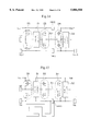
- An example of a conventional semiconductor unit shown in FIG. 1 has an analog section as a first circuit and a digital section as a second circuit.
- the analog section includes an analog circuit 1, an output circuit 3 and an input protective circuit 5.
- the digital section includes a digital circuit 2 and an input circuit 4.
- the first and second circuits are connected with each other through a signal line S1 between the output circuit 3 and the input circuit 4 of the respective first and second circuits.
- An electric source voltage applied to the analog section is supplied through electric source lines Vdd1 and Vss1, and an electric source voltage applied to the digital section is supplied through electric source lines Vdd2 and Vss2.
- the electric source line Vdd1 is separated from the electric source line Vdd2, and the electric source line Vss1 is separated from the electric source line Vss2.
- a signal is output from the analog circuit 1 through the output circuit 3 to the digital section. Thereafter, the signal is input to the input circuit 4, an inverter, through the signal line S1 and is transmitted to the digital circuit 2.
- FIG. 2 another conventional semiconductor unit shown in FIG. 2 has an analog section composed of an analog circuit 11, an output circuit 13 and an input protective circuit 15 and a digital section composed of a digital circuit 12 and an input circuit 14.
- the first and second circuits are connected with each other through a signal line S1.
- An electric source voltage applied to the analog section is supplied through electric source lines Vdd and Vss, and an electric source voltage applied to the digital section is supplied through the same electric source lines Vdd and Vss.
- the path for the electric source line Vss takes a long way around because of a design requirement and the electric source line Vss becomes lengthy.
- An object of the present invention is to provide, with due consideration to the drawbacks of such a conventional semiconductor unit, a semiconductor unit in which break down of an element caused by an electric potential difference between two electric source systems is suppressed.
- a gate electric potential of a metal-oxide-semiconductor (MOS) transistor Q1 in the inverter of the input circuit 4 is excessively increased to increase a voltage between a gate and a source of the MOS transistor Q1 excessively increased. This increased voltage breaks down a gate oxide film of the MOS transistor Q1.
- MOS metal-oxide-semiconductor
- a semiconductor unit comprises a first circuit, a second circuit, a signal line, and a protective circuit for electrically connecting a first electric source line of a low electric potential side (or a high electric potential side) and a second electric source line of a low electric potential side (or a high electric potential side) in cases where an electric potential difference between the first electric source line of the low electric potential side (or the high electric potential side) and the second electric source line of the low electric potential side (or the high electric potential side) exceeds a prescribed value.
- the protective circuit electrically connects the first electric source line of the low electric potential side (or the high electric potential side) and the second electric source line of the low electric potential side (or the high electric potential side), so that the electric potential of the first electric source line of the low electric potential side (or the high electric potential side) becomes equal to that of the second electric source line of the low electric potential side (or the high electric potential side).
- another semiconductor unit comprises a first circuit, a second circuit, a signal line, and a protective circuit for electrically connecting the signal line and an electric source line of a low electric potential side (or a high electric potential side) in cases where an electric potential difference between the signal line and the electric source line of the low electric potential side (or the high electric potential side) exceeds a prescribed value.
- the protective circuit electrically connects the signal line and the electric source line of the low electric potential side (or the high electric potential side), so that the electric potential of the electric source line of the low electric potential side (or the high electric potential side) becomes equal to that of the signal line.
- the protective circuit is provided for the semiconductor unit, the current is split by the protective circuit, and a major part of the current passes through the electric source line of the low electric potential side (or the high electric potential side). Therefore, because any large amount of current does not pass through the signal line, break down of input and output circuits connected to the signal line can be prevented.
- a protective circuit is provided across a lengthy section of an electric source line between first and second circuits so as to short cut the lengthy section when an electric potential across the lengthy section exceeds a prescribed value.
- FIG. 1 is an electrical diagram of a conventional semiconductor unit.
- FIG. 2 is an electrical diagram of another conventional semiconductor unit.
- FIG. 3 is an electrical diagram of a semiconductor unit according to a first embodiment of the present invention.
- FIG. 4 is a diagram of a first type of protective circuit (HK1 or HK2) according to the first embodiment of the present invention.
- FIG. 5 is a diagram of a second type of protective circuit (HK1 or HK2) according to the first embodiment of the present invention.
- FIG. 6 is a diagram of a third type of protective circuit (HK1 or HK2) according to the first embodiment of the present invention.
- FIG. 7 is a diagram of a fourth type of protective circuit (HK1 or HK2) according to the first embodiment of the present invention.
- FIG. 8 is a diagram of a fifth type of protective circuit (HK1 or HK2) according to the first embodiment of the present invention.
- FIG. 9 is a diagram of a sixth type of protective circuit (HK1 or HK2) according to the first embodiment of the present invention.
- FIG. 10 is a diagram of a seventh type of protective circuit (HK1 or HK2) according to the first embodiment of the present invention.
- FIG. 11 is a diagram of an eighth type of protective circuit (HK1 or HK2) according to the first embodiment of the present invention.
- FIG. 12 is a diagram of a ninth type of protective circuit (HK1 or HK2) according to the first embodiment of the present invention.
- FIG. 13 is a diagram of a second variation of the semiconductor unit according to the first embodiment of the present invention.
- FIG. 14 is a diagram of a third variation of the semiconductor unit according to the first embodiment of the present invention.
- FIG. 15 is an electrical diagram of a semiconductor unit according to a second embodiment of the present invention.
- FIG. 16 is a diagram of a second variation of the semiconductor unit according to the second embodiment of the present invention.
- FIG. 17 is a diagram of a semiconductor unit according to a third embodiment of the present invention.
- FIG. 18 is a diagram of a first type of a protective circuit (HK3) according to the third embodiment of the present invention.
- FIG. 19 is a diagram of a second type of protective circuit (HK3) according to the third embodiment of the present invention.
- FIG. 20 is a diagram of a third type of protective circuit (HK3) according to the third embodiment of the present invention.
- FIG. 21 is a diagram of a second variation of the semiconductor unit according to the third embodiment of the present invention.
- FIG. 22 is a diagram of a first type of a protective circuit (HK4) according to the third embodiment of the present invention.
- FIG. 23 is a diagram of a second type of protective circuit (HK4) according to the third embodiment of the present invention.
- FIG. 24 is a diagram of a third type of protective circuit (HK4) according to the third embodiment of the present invention.
- FIG. 25 is a diagram of a third variation of the semiconductor unit according to the third embodiment of the present invention.
- FIG. 26 is an electrical diagram of a semiconductor unit according to a fourth embodiment of the present invention.
- FIG. 27 is a diagram of a second variation of the semiconductor unit according to the fourth embodiment of the present invention.
- FIG. 28 is an electrical diagram of a semiconductor unit according to a fifth embodiment of the present invention.
- FIG. 29 is a diagram of a second variation of the semiconductor unit according to the fifth embodiment of the present invention.
- FIG. 30 is a diagram of a third variation of the semiconductor unit according to the fifth embodiment of the present invention.
- a semiconductor unit comprises a digital unit and an analog unit in the same manner as a semiconductor memory or the like.
- the analog unit comprises an analog circuit 21, an output circuit 23 and an input protective circuit 25.
- the digital unit comprises a digital circuit 22 and an input circuit 24.
- the analog unit and the digital unit are connected with each other through a signal line S11.
- An electric source voltage applied to the analog unit is supplied through each of electric source lines Vdd1 and Vss1, and an electric source voltage applied to the digital unit is supplied through each of electric source lines Vdd2 and Vss2.
- the electric source line Vdd1 is separated from the electric source line Vdd2, and the electric source line Vss1 and the electric source line Vss2 are connected to each other through a protective circuit HK1.
- the analog unit is an example of a first circuit
- the digital unit is an example of a second circuit.
- the electric source line Vdd1 is an example of a first electric source line of a high electric potential side
- the electric source line Vss1 is an example of a first electric source line of a low electric potential side
- the electric source line Vdd2 is an example of a second electric source line of a high electric potential side
- the electric source line Vss2 is an example of a second electric source line of a low electric potential side.
- a digital circuit can be the first circuit and an analog circuit can be the second circuit.
- digital circuits can be the first and second circuits or analog circuits can be the first and second circuits.
- the protective circuit HK1 functions to electrically connect the electric source line Vss1 and the electric source line Vss2 in cases where an electric potential difference between the electric source lines Vss1 and Vss2 exceeds a prescribed value. That is, the protective circuit HK1 is a switching circuit which, when operated, sets the electric source lines Vss1 and Vss2 to the same electric potential.
- a signal generated in the analog circuit 21 is output to the signal line S11 through the output circuit 23 and is transmitted to the digital circuit 22 through the input circuit 24 made of an inverter.
- an electric potential difference between the electric source lines Vss1 and Vss2 is induced to become large.
- the protective circuit HK1 is operated, the electric source lines Vss1 and Vss2 are electrically connected to each other, and the electric source lines Vss1 and Vss2 are set to the same electric potential.
- the protective circuit HK1 shown in FIGS. 4 to 6 is one or more n-channel MOS transistors
- the protective circuit HK1 shown in FIGS. 7 to 9 is one or more p-channel MOS transistors
- the protective circuit HK1 shown in FIGS. 10 to 12 is one or more diodes.
- the electric source line Vss1 and the electric source line Vss2 are electrically connected to each other in cases where an electric potential difference between the electric source lines Vss1 and Vss2 exceeds a prescribed value, so that the electric source lines Vss1 and Vss2 are held to almost the same electric potential.
- the configuration of the protective circuit HK1 is not limited to the examples shown in FIGS. 4 to 12.
- the protective circuit HK1 can be made by connecting two or more examples in series or in parallel.
- the protective circuit HK1 can be composed of one or more bipolar transistors such as PNP type transistors or NPN transistors.
- any circuit can be used as the protective circuit HK1 on condition that two electric source lines are electrically connected to set the two electric source lines to the same electric potential in cases where an electric potential difference between the two electric source lines exceeds a prescribed value.
- the protective circuit HK1 shown in FIG. 10 is described as an example.
- the protective circuit HK1 is composed of a single diode. In this circuit, when an electric potential difference between the electric source lines Vss1 and Vss2 is equal to or lower than about 0.6 V, the electric source lines Vss1 and Vss2 are not electrically connected to each other.
- the electric source lines Vss1 and Vss2 are electrically connected to each other, and the electric source lines Vss1 and Vss2 are set to almost the same electric potential in the same manner.
- the protective circuit HK1 is arranged between the electric source lines Vss1 and Vss2 of the low electric potential side.
- the present invention is not limited to the protective circuit HK1. That is, as shown in FIG. 13, a protective circuit HK2 can be arranged between the electric source lines Vdd1 and Vdd2 of the high electric potential side. Also, as shown in FIG. 14, the protective circuit HK1 can be arranged between the electric source lines Vss1 and Vss2 of the low electric potential side and the protective circuit HK2 can be arranged between the electric source lines Vdd1 and Vdd2 of the high electric potential side be provided for the semiconductor unit.
- a semiconductor unit comprises an analog unit and a digital unit.
- the analog unit comprises an analog circuit 31, an input protective circuit 35 connected to the analog circuit 31, and an output circuit 33 connected to the analog circuit 31.
- the digital unit comprises a digital circuit 32 and an input circuit 34 connected to the digital circuit 32.
- An electric source line Vss of a low electric potential side and an electric source line Vdd of a high electric potential side are connected to the circuits 31 to 35, and a signal line S11 connects the output circuit 33 and the input circuit 34.
- the electric source line Vss takes a long way around another section (not shown) because of a design requirement, so that the electric source line Vss between the analog and digital units becomes lengthy.
- the protective circuit HK1 is connected across this lengthy section of the electric source line Vss between the analog unit and the digital unit to short-cut the electric source line Vss.
- a signal generated in the analog circuit 31 is output to the signal line S11 through the output circuit 33 and is transmitted to the digital circuit 32 through the input circuit 34 made of an inverter.
- an electric potential difference instantaneously occurring between the portion of the electric source line Vss close to the analog circuit 31 and the portion of the electric source line Vss close to the digital circuit 32 and exceeding a prescribed electric potential difference operates the protective circuit HK1 to short-cut the lengthy portion of the electric source line Vss between the analog and digital circuits, so that an electric potential of the portion of the electric source line Vss close to the digital circuit 32 is rapidly increased to the prescribed electric source voltage. Therefore, the break down of the gate insulating film of the MOS transistor Q1 can be prevented.
- the protective circuit HK1 is arranged on the electric source lines Vss of the low electric potential side.
- a protective circuit HK2, FIG. 16 can be connected to the electric source line Vdd of the high electric potential side between the analog unit and the digital unit to short-cut the electric source line Vdd.
- the protective circuit HK1 can be connected to the electric source line Vss of the low electric potential side and the protective circuit HK2 can be connected to the electric source line Vdd of the high electric potential side in the semiconductor unit.
- each of the protective circuits HK1 and HK2 is shown in FIGS. 4 to 12 in the same manner as in the first embodiment.
- a semiconductor unit according to the third embodiment comprises an analog unit and a digital unit in the same manner as the semiconductor memory.
- the analog unit of the semiconductor unit according to the third embodiment comprises an analog circuit 41, an output circuit 43 and an input protective circuit 45
- the digital unit of the semiconductor unit comprises a digital circuit 42 and an input circuit 44.
- a signal line S11 connects the output circuit 43 of the analog unit and the input circuit 44 of the digital unit.
- An electric source voltage applied to the analog unit is supplied through each of electric source lines Vdd1 and Vss1, and an electric source voltage applied to the digital unit is supplied through each of electric source lines Vdd2 and Vss2.
- the electric source line Vdd1 is separated from the electric source line Vdd2, and the electric source line Vss1 is separated from the electric source line Vss2.
- the analog unit is an example of a first circuit
- the digital unit is an example of a second circuit.
- the electric source line Vdd1 is an example of a first electric source line of a high electric potential side
- the electric source line Vss1 is an example of a first electric source line of a low electric potential side
- the electric source line Vdd2 is an example of a second electric source line of a high electric potential side
- the electric source line Vss2 is an example of a second electric source line of a low electric potential side.
- the semiconductor unit further comprises a protective circuit HK3 connecting the electric source line Vss2 and the signal line S11.
- a protective circuit HK3 connecting the electric source line Vss2 and the signal line S11.
- a signal generated in the analog circuit 41 is output to the signal line S11 through the output circuit 43 and is transmitted to the digital circuit 42 through the input circuit 44 made of an inverter.
- FIGS. 18 to 20 A plurality of examples of the protective circuit HK3 are shown in FIGS. 18 to 20. Also, the protective circuit HK3 can be made by connecting two or more examples in series or in parallel. Also, the protective circuit HK3 can be one or more bipolar transistors such as PNP type transistors or NPN transistors. In conclusion, any circuit can be used as the protective circuit HK3 on condition that one electric source line and one signal line are electrically connected to set the electric source line and the signal line to the same electric potential in cases where an electric potential difference between the electric source line and the signal line exceeds a prescribed value.
- the protective circuit HK3 is arranged to electrically connect the electric source line Vss2 of the low electric potential side and the signal line S11.
- the present invention is not limited to such placement of the protective circuit HK3.
- a protective circuit HK4 can be arranged to electrically connect the electric source line Vdd2 of the high electric potential side and the signal line S11.
- the protective circuit HK3 can electrically connect the electric source line Vss2 of the low electric potential side and the signal line S11 and the protective circuit HK4 can electrically connect the electric source line Vdd2 of the high electric potential side and the signal line S11.
- FIGS. 22 to 24 A plurality of examples of the protective circuit HK4 are shown in FIGS. 22 to 24. Also, the protective circuit HK4 can be made by connecting two or more examples in series or in parallel. Also, the protective circuit HK4 can be one or more bipolar transistors such as PNP type transistors or NPN transistors. In conclusion, any circuit can be used as the protective circuit HK3 on condition that one electric source line and one signal line are electrically connected to set the electric source line and the signal line to the same electric potential in cases where an electric potential difference between the electric source line and the signal line exceeds a prescribed value.
- a semiconductor unit comprises an analog unit and a digital unit.
- the analog unit comprises an analog circuit 51, an input protective circuit 55 connected to the analog circuit 51, and an output circuit 53 connected to the analog circuit 51.
- the digital unit comprises a digital circuit 52 and an input circuit 54 connected to the digital circuit 52.
- An electric source line Vss of a low electric potential side and an electric source line Vdd of a high electric potential side are respectively connected to the circuits 51 to 55, and a signal line S11 connects the output circuit 53 and the input circuit 54.
- the electric source line Vss takes a long way around another section (not shown) because of a design requirement, so that the section of the electric source line Vss between the analog and digital units becomes lengthy.
- the semiconductor unit further comprises the protective circuit HK3 connecting the electric source line Vss close to the digital circuit 52 and the signal line S11, in the same manner as in the third embodiment.
- a signal generated in the analog circuit 51 is output to the signal line S11 through the output circuit 53 and is transmitted to the digital circuit 52 through the input circuit 54 made of an inverter.
- the protective circuit HK3 is operated to electrically connect the electric source line Vss close to the digital circuit 52 and the signal line S11, so that the portion of the electric source line Vss close to the digital circuit 52 and the signal line S11 are set to the same electric potential.
- the protective circuit HK3 is arranged to electrically connect the electric source line Vss close to the digital circuit 52 and the signal line S11.
- the protective circuit HK3 can be arranged to electrically connect the electric source line Vdd close to the digital circuit 52 and the signal line S11.
- both the protective circuit HK3 electrically connects the electric source line Vss close to the digital circuit 52 and the signal line S11
- the protective circuit HK4 electrically connects the electric source line Vdd close to the digital circuit 52 and the signal line S11 for the semiconductor unit.
- a semiconductor unit comprises an analog unit and a digital unit.
- the analog unit comprises an analog circuit 61, an input protective circuit 65 connected to the analog circuit 61, and an output circuit 63 connected to the analog circuit 61.
- the digital unit comprises a digital circuit 62 and an input circuit 64 connected to the digital circuit 62.
- a signal line S11 connects the output circuit 63 and the input circuit 64.
- An electric source voltage applied to the analog unit is supplied through each of electric source lines Vdd1 and Vss1, and an electric source voltage applied to the digital unit is supplied through each of electric source lines Vdd2 and Vss2.
- the analog unit is an example of a first circuit
- the digital unit is an example of a second circuit.
- the electric source line Vdd1 is an example of a first electric source line of a high electric potential side
- the electric source line Vss1 is an example of a first electric source line of a low electric potential side
- the electric source line Vdd2 is an example of a second electric source line of a high electric potential side
- the electric source line Vss2 is an example of a second electric source line of a low electric potential side.
- the semiconductor unit further comprises a protective circuit HK5 through which the electric source lines Vdd1, Vdd2, Vss1 and Vss2 are connected to each other.
- the protective circuit HK5 comprises a first p-channel MOS transistor T1 in which a drain is connected with the electric source line Vdd1, a source is connected with the electric source line Vss2 and a gate and the drain are electrically connected, a second p-channel MOS transistor T2 in which a source is connected with the electric source line Vss1, a drain is connected with the electric source line Vdd2 and a gate and the drain are electrically connected, a third p-channel MOS transistor T3 in which a drain is connected with the electric source line Vdd1, a source is connected with the electric source line Vss1 and a gate and the drain are electrically connected, and a fourth p-channel MOS transistor T4 in which a drain is connected with the electric source line Vdd2, a source is connected with the electric source line Vss
- a signal generated in the analog circuit 61 is output to the signal line S11 through the output circuit 63 and is transmitted to the digital circuit 62 through the input circuit 64 made of an inverter.
- the protective circuit HK5 is equivalent to a diode circuit shown in FIG. 30, the MOS transistors T1 to T4 are turned off in the normal operation, and the electric source lines Vdd1, Vdd2, Vss1 and Vss2 are electrically separated from each other.
- the electric source lines Vdd1 and Vss2 are electrically separated from each other by the first MOS transistor T1
- the electric source lines Vdd2 and Vss1 are electrically separated from each other by the second MOS transistor T2
- the electric source lines Vdd1 and Vss1 are electrically separated from each other by the third MOS transistor T3
- the electric source lines Vdd2 and Vss2 are electrically separated from each other by the fourth MOS transistor T4.
- a part of the surge current SR passes through a first route connecting the electric source line Vss1, the second MOS transistor T2, the electric source line Vdd2, the fourth MOS transistor T4 and the electric source line Vss2, and another part of the surge current SR passes through a second route connecting the electric source line Vss1, the third MOS transistor T3, the electric source line Vdd1, the first MOS transistor T1 and the electric source line Vss2. Accordingly, the electric source lines Vss1 and Vss2 are set to almost the same electric potential, and break down of a gate oxide film of a MOS transistor Q1 of the input circuit 64 can be prevented.
- the electric source lines Vdd1 and Vdd2 are set to almost the same electric potential in the same manner, and break down of the gate oxide film of the MOS transistor Q1 can be prevented.
- the p-channel MOS transistors T1 to T4 are used for the protective circuit HK5.
- the protective circuit HK5 comprise four n-channel MOS transistors T11 to T14.
- gates of the n-channel MOS transistors T12 and T13 are electrically connected with the electric source line Vss1
- gates of the n-channel MOS transistors T11 and T14 are electrically connected with the electric source line Vss 2.
- a surge current SR when supplied to the applied terminal NT or a terminal of the electric source line Vss1, a part of the surge current SR passes through a first route connecting the electric source line Vss1, the MOS transistor T12 the electric source line Vdd2, the MOS transistor T14 and the electric source line Vss2, and another part of the surge current SR passes through second route connecting the electric source line Vss1, the MOS transistor T13, the electric source line Vdd1, the MOS transistor T11 and the electric source line Vss2. Accordingly, the electric source lines Vss1 and Vss2 are set to almost the same electric potential, and break down of the gate oxide film of the MOS transistor Q1 can be prevented.
- the diodes D1 to D4 be used in place of the MOS transistors T1 to T4 (or T11 to T14). That is, a cathode of the diode D1 is connected with the electric source line Vdd1, an anode of the diode D1 is connected with the electric source line Vss2, a cathode of the diode D2 is connected with the electric source line Vdd2, an anode of the diode D2 is connected with the electric source line Vss1, a cathode of the diode D3 is connected with the electric source line Vdd1, an anode of the diode D3 is connected with the electric source line Vss1, a cathode of the diode D4 is connected with the electric source line Vss2, and an anode of the diode D4 is connected with the electric source line Vdd2.
Landscapes
- Engineering & Computer Science (AREA)
- Physics & Mathematics (AREA)
- Computer Hardware Design (AREA)
- Computing Systems (AREA)
- General Engineering & Computer Science (AREA)
- Mathematical Physics (AREA)
- Power Engineering (AREA)
- Condensed Matter Physics & Semiconductors (AREA)
- General Physics & Mathematics (AREA)
- Microelectronics & Electronic Packaging (AREA)
- Semiconductor Integrated Circuits (AREA)
- Insulated Gate Type Field-Effect Transistor (AREA)
Abstract
Description
Claims (24)
Applications Claiming Priority (6)
| Application Number | Priority Date | Filing Date | Title |
|---|---|---|---|
| JP22438195 | 1995-08-31 | ||
| JP7-224381 | 1995-08-31 | ||
| JP26709795 | 1995-10-16 | ||
| JP7-267097 | 1995-10-16 | ||
| JP13537296A JP3229809B2 (en) | 1995-08-31 | 1996-05-29 | Semiconductor device |
| JP8-135372 | 1996-05-29 |
Publications (1)
| Publication Number | Publication Date |
|---|---|
| US5886558A true US5886558A (en) | 1999-03-23 |
Family
ID=27317071
Family Applications (1)
| Application Number | Title | Priority Date | Filing Date |
|---|---|---|---|
| US08/703,884 Expired - Lifetime US5886558A (en) | 1995-08-31 | 1996-08-27 | Semiconductor unit |
Country Status (3)
| Country | Link |
|---|---|
| US (1) | US5886558A (en) |
| JP (1) | JP3229809B2 (en) |
| KR (1) | KR100250018B1 (en) |
Cited By (21)
| Publication number | Priority date | Publication date | Assignee | Title |
|---|---|---|---|---|
| US6271706B1 (en) * | 1998-01-22 | 2001-08-07 | Intel Corporation | Divided voltage de-coupling structure |
| US6404016B1 (en) * | 1999-05-21 | 2002-06-11 | Sanyo Electric Co. Ltd. | Semiconductor device |
| US20030227304A1 (en) * | 2002-06-10 | 2003-12-11 | Hitachi, Ltd. | Semiconductor integrated circuit device |
| US20040169541A1 (en) * | 2003-02-27 | 2004-09-02 | Nec Electronics Corporation | Semiconductor integrated device and apparatus for designing the same |
| US20050190513A1 (en) * | 2004-03-01 | 2005-09-01 | Omron Corporation | Surge suppression circuit |
| US20050201031A1 (en) * | 2004-03-10 | 2005-09-15 | Nec Electronics Corporation | Protection circuit in semiconductor circuit device comprising a plurality of chips |
| US20060103421A1 (en) * | 2003-02-27 | 2006-05-18 | Morihisa Hirata | System-in-package type semiconductor device |
| US20060114047A1 (en) * | 2004-11-26 | 2006-06-01 | Nec Electronics Corporation | Semiconductor unit |
| US20060202679A1 (en) * | 2003-12-18 | 2006-09-14 | Hitachi, Ltd. | Displacement sensor |
| US20070025033A1 (en) * | 2005-07-28 | 2007-02-01 | Oki Electric Industry Co., Ltd. | Semiconductor device |
| US20070182444A1 (en) * | 2006-01-24 | 2007-08-09 | Nec Electronics Corporation | Semiconductor integrated circuit device |
| CN100420993C (en) * | 2005-04-28 | 2008-09-24 | 乐金显示有限公司 | Integrated chip and planel display device using same |
| US20090205649A1 (en) * | 2008-02-19 | 2009-08-20 | Portaero, Inc. | Multi-layer pneumostoma management system and methods for treatment of chronic obstructive pulmonary disease |
| CN102117803A (en) * | 2009-12-31 | 2011-07-06 | 无锡中星微电子有限公司 | Chip provided with high electrostatic discharge performance |
| US20130077196A1 (en) * | 2011-09-28 | 2013-03-28 | Texas Instruments Incorporated | ESD Robust Level Shifter |
| US8803237B2 (en) | 2009-04-09 | 2014-08-12 | Renesas Electronics Corporation | Semiconductor device |
| US20160322115A1 (en) * | 2015-04-29 | 2016-11-03 | Boe Technology Group Co., Ltd. | Shift Register Unit, Driving Method Thereof, Gate Driving Circuit and Display Apparatus |
| US9941270B2 (en) | 2015-01-08 | 2018-04-10 | Panasonic Intellectual Property Management Co., Ltd. | Semiconductor device and design method of same |
| CN111180440A (en) * | 2020-01-20 | 2020-05-19 | 杭州电子科技大学 | Single-phase direct current motor driving chip and chip drawing method |
| EP4055394A4 (en) * | 2019-11-05 | 2023-12-13 | FormFactor, Inc. | Probe systems and methods for testing a device under test |
| US11990465B2 (en) | 2020-07-15 | 2024-05-21 | Renesas Electronics Corporation | Semiconductor device |
Families Citing this family (9)
| Publication number | Priority date | Publication date | Assignee | Title |
|---|---|---|---|---|
| JP3302665B2 (en) | 1999-10-25 | 2002-07-15 | ローム株式会社 | Semiconductor integrated circuit device |
| JP3786608B2 (en) * | 2002-01-28 | 2006-06-14 | 株式会社ルネサステクノロジ | Semiconductor integrated circuit device |
| JP3495031B2 (en) | 2002-05-28 | 2004-02-09 | 沖電気工業株式会社 | ESD protection circuit for semiconductor devices |
| JP3713013B2 (en) * | 2002-12-06 | 2005-11-02 | 松下電器産業株式会社 | Manufacturing method of semiconductor integrated circuit device |
| JP2006203801A (en) * | 2005-01-24 | 2006-08-03 | Fujitsu Ltd | Buffer circuit and integrated circuit |
| JP4806540B2 (en) | 2005-05-18 | 2011-11-02 | ルネサスエレクトロニクス株式会社 | Semiconductor integrated circuit device |
| JP4987447B2 (en) | 2006-11-30 | 2012-07-25 | オンセミコンダクター・トレーディング・リミテッド | Semiconductor integrated circuit |
| JP5175597B2 (en) * | 2007-11-12 | 2013-04-03 | エスケーハイニックス株式会社 | Semiconductor integrated circuit |
| JP5576674B2 (en) * | 2010-02-23 | 2014-08-20 | ルネサスエレクトロニクス株式会社 | Semiconductor device |
Citations (9)
| Publication number | Priority date | Publication date | Assignee | Title |
|---|---|---|---|---|
| US4847518A (en) * | 1987-11-13 | 1989-07-11 | Harris Semiconductor Patents, Inc. | CMOS voltage divider circuits |
| US4958132A (en) * | 1989-05-09 | 1990-09-18 | Advanced Micro Devices, Inc. | Complementary metal-oxide-semiconductor translator |
| JPH048115A (en) * | 1990-04-25 | 1992-01-13 | Oki Electric Ind Co Ltd | Antistatic circuit |
| US5272399A (en) * | 1992-02-25 | 1993-12-21 | Siemens Aktiengesellschaft | Circuit limiting the load current of a power MOSFET |
| US5280200A (en) * | 1989-04-10 | 1994-01-18 | Tarng Min M | Pipelined buffer for analog signal and power supply |
| US5440163A (en) * | 1992-09-01 | 1995-08-08 | Nec Corporation | CMOS ESD protection structure |
| US5486716A (en) * | 1991-05-14 | 1996-01-23 | Seiko Instruments Inc. | Semiconductor integrated circuit device with electrostatic damage protection |
| US5574395A (en) * | 1994-06-17 | 1996-11-12 | Mitsubishi Denki Kabushiki Kaisha | Semiconductor circuit |
| US5610550A (en) * | 1993-01-29 | 1997-03-11 | Mitsubishi Denki Kabushiki Kaisha | Intermediate potential generator stably providing an internal voltage precisely held at a predeterminded intermediate potential level with reduced current consumption |
Family Cites Families (2)
| Publication number | Priority date | Publication date | Assignee | Title |
|---|---|---|---|---|
| JP2598147B2 (en) * | 1990-02-09 | 1997-04-09 | シャープ株式会社 | Semiconductor integrated circuit |
| JPH0613555A (en) * | 1992-06-25 | 1994-01-21 | Toshiba Corp | Electrostatic damage preventing circuit |
-
1996
- 1996-05-29 JP JP13537296A patent/JP3229809B2/en not_active Expired - Fee Related
- 1996-08-27 US US08/703,884 patent/US5886558A/en not_active Expired - Lifetime
- 1996-08-30 KR KR1019960036708A patent/KR100250018B1/en not_active IP Right Cessation
Patent Citations (9)
| Publication number | Priority date | Publication date | Assignee | Title |
|---|---|---|---|---|
| US4847518A (en) * | 1987-11-13 | 1989-07-11 | Harris Semiconductor Patents, Inc. | CMOS voltage divider circuits |
| US5280200A (en) * | 1989-04-10 | 1994-01-18 | Tarng Min M | Pipelined buffer for analog signal and power supply |
| US4958132A (en) * | 1989-05-09 | 1990-09-18 | Advanced Micro Devices, Inc. | Complementary metal-oxide-semiconductor translator |
| JPH048115A (en) * | 1990-04-25 | 1992-01-13 | Oki Electric Ind Co Ltd | Antistatic circuit |
| US5486716A (en) * | 1991-05-14 | 1996-01-23 | Seiko Instruments Inc. | Semiconductor integrated circuit device with electrostatic damage protection |
| US5272399A (en) * | 1992-02-25 | 1993-12-21 | Siemens Aktiengesellschaft | Circuit limiting the load current of a power MOSFET |
| US5440163A (en) * | 1992-09-01 | 1995-08-08 | Nec Corporation | CMOS ESD protection structure |
| US5610550A (en) * | 1993-01-29 | 1997-03-11 | Mitsubishi Denki Kabushiki Kaisha | Intermediate potential generator stably providing an internal voltage precisely held at a predeterminded intermediate potential level with reduced current consumption |
| US5574395A (en) * | 1994-06-17 | 1996-11-12 | Mitsubishi Denki Kabushiki Kaisha | Semiconductor circuit |
Non-Patent Citations (1)
| Title |
|---|
| IBM Tech Disc Bul., vol. 38, No. 12 327/314, Protect diode scheme for chips requiring isolated power/ground planes for internal/external noise isolation, Dec. 1995. * |
Cited By (42)
| Publication number | Priority date | Publication date | Assignee | Title |
|---|---|---|---|---|
| US6271706B1 (en) * | 1998-01-22 | 2001-08-07 | Intel Corporation | Divided voltage de-coupling structure |
| US6404016B1 (en) * | 1999-05-21 | 2002-06-11 | Sanyo Electric Co. Ltd. | Semiconductor device |
| US20030227304A1 (en) * | 2002-06-10 | 2003-12-11 | Hitachi, Ltd. | Semiconductor integrated circuit device |
| CN1326242C (en) * | 2002-06-10 | 2007-07-11 | 株式会社日立制作所 | Semiconductor integrated circuit device |
| US6828842B2 (en) * | 2002-06-10 | 2004-12-07 | Hitachi, Ltd. | Semiconductor integrated circuit device |
| US7631279B2 (en) * | 2003-02-27 | 2009-12-08 | Nec Electronics Corporation | Semiconductor integrated device and apparatus for designing the same |
| US20090077517A1 (en) * | 2003-02-27 | 2009-03-19 | Morihisa Hirata | Semiconductor intergrated device and apparatus for designing the same |
| US20060103421A1 (en) * | 2003-02-27 | 2006-05-18 | Morihisa Hirata | System-in-package type semiconductor device |
| US7312517B2 (en) | 2003-02-27 | 2007-12-25 | Nec Electronics Corporation | System-in-package type semiconductor device |
| US7076757B2 (en) | 2003-02-27 | 2006-07-11 | Nec Electronics Corporation | Semiconductor integrated device and apparatus for designing the same |
| US20090077516A1 (en) * | 2003-02-27 | 2009-03-19 | Morihisa Hirata | Semiconductor integrated device and apparatus for designing the same |
| US20060218518A1 (en) * | 2003-02-27 | 2006-09-28 | Morihisa Hirata | Semiconductor integrated device and apparatus for designing the same |
| US7624365B2 (en) * | 2003-02-27 | 2009-11-24 | Nec Electronics Corporation | Semiconductor integrated device and apparatus for designing the same |
| US20040169541A1 (en) * | 2003-02-27 | 2004-09-02 | Nec Electronics Corporation | Semiconductor integrated device and apparatus for designing the same |
| US7552404B2 (en) * | 2003-02-27 | 2009-06-23 | Nec Electronics Corporation | Semiconductor integrated device and apparatus for designing the same |
| CN100334729C (en) * | 2003-02-27 | 2007-08-29 | 恩益禧电子股份有限公司 | Semiconductor integrated device and apparatus for designing the same |
| US20060202679A1 (en) * | 2003-12-18 | 2006-09-14 | Hitachi, Ltd. | Displacement sensor |
| US7622913B2 (en) * | 2003-12-18 | 2009-11-24 | Hitachi, Ltd. | Displacement sensor |
| US20050190513A1 (en) * | 2004-03-01 | 2005-09-01 | Omron Corporation | Surge suppression circuit |
| US7561390B2 (en) | 2004-03-10 | 2009-07-14 | Nec Electronics Corporation | Protection circuit in semiconductor circuit device comprising a plurality of chips |
| US20050201031A1 (en) * | 2004-03-10 | 2005-09-15 | Nec Electronics Corporation | Protection circuit in semiconductor circuit device comprising a plurality of chips |
| US7495872B2 (en) | 2004-11-26 | 2009-02-24 | Nec Electronics Corporation | Semiconductor unit |
| CN100448006C (en) * | 2004-11-26 | 2008-12-31 | 恩益禧电子股份有限公司 | Semiconductor unit |
| US20060114047A1 (en) * | 2004-11-26 | 2006-06-01 | Nec Electronics Corporation | Semiconductor unit |
| CN100420993C (en) * | 2005-04-28 | 2008-09-24 | 乐金显示有限公司 | Integrated chip and planel display device using same |
| US20070025033A1 (en) * | 2005-07-28 | 2007-02-01 | Oki Electric Industry Co., Ltd. | Semiconductor device |
| US7489486B2 (en) | 2005-07-28 | 2009-02-10 | Oki Electric Industry Co., Ltd. | Semiconductor device |
| US8270132B2 (en) | 2006-01-24 | 2012-09-18 | Renesas Electronics Corporation | Semiconductor device with a plurality of power supply systems |
| US20070182444A1 (en) * | 2006-01-24 | 2007-08-09 | Nec Electronics Corporation | Semiconductor integrated circuit device |
| US7869174B2 (en) | 2006-01-24 | 2011-01-11 | Renesas Electronics Corporation | Semiconductor device with a plurality of power supply systems |
| US8749932B2 (en) | 2006-01-24 | 2014-06-10 | Renesas Electronics Corporation | Semiconductor device with a plurality of power supply systems |
| US20090205649A1 (en) * | 2008-02-19 | 2009-08-20 | Portaero, Inc. | Multi-layer pneumostoma management system and methods for treatment of chronic obstructive pulmonary disease |
| US8803237B2 (en) | 2009-04-09 | 2014-08-12 | Renesas Electronics Corporation | Semiconductor device |
| CN102117803A (en) * | 2009-12-31 | 2011-07-06 | 无锡中星微电子有限公司 | Chip provided with high electrostatic discharge performance |
| CN102117803B (en) * | 2009-12-31 | 2014-10-08 | 无锡中星微电子有限公司 | Chip provided with high electrostatic discharge performance |
| US20130077196A1 (en) * | 2011-09-28 | 2013-03-28 | Texas Instruments Incorporated | ESD Robust Level Shifter |
| US9154133B2 (en) * | 2011-09-28 | 2015-10-06 | Texas Instruments Incorporated | ESD robust level shifter |
| US9941270B2 (en) | 2015-01-08 | 2018-04-10 | Panasonic Intellectual Property Management Co., Ltd. | Semiconductor device and design method of same |
| US20160322115A1 (en) * | 2015-04-29 | 2016-11-03 | Boe Technology Group Co., Ltd. | Shift Register Unit, Driving Method Thereof, Gate Driving Circuit and Display Apparatus |
| EP4055394A4 (en) * | 2019-11-05 | 2023-12-13 | FormFactor, Inc. | Probe systems and methods for testing a device under test |
| CN111180440A (en) * | 2020-01-20 | 2020-05-19 | 杭州电子科技大学 | Single-phase direct current motor driving chip and chip drawing method |
| US11990465B2 (en) | 2020-07-15 | 2024-05-21 | Renesas Electronics Corporation | Semiconductor device |
Also Published As
| Publication number | Publication date |
|---|---|
| JP3229809B2 (en) | 2001-11-19 |
| KR970013425A (en) | 1997-03-29 |
| JPH09172146A (en) | 1997-06-30 |
| KR100250018B1 (en) | 2000-03-15 |
Similar Documents
| Publication | Publication Date | Title |
|---|---|---|
| US5886558A (en) | Semiconductor unit | |
| US5532621A (en) | Output buffer circuit, input buffer circuit and bi-directional buffer circuit for plural voltage systems | |
| EP0575062B1 (en) | ESD protection of output buffers | |
| US5852375A (en) | 5v tolerant I/O circuit | |
| US4481432A (en) | Programmable output buffer | |
| KR0128508B1 (en) | Integrated circuit with esd protection of output buffers | |
| US5639680A (en) | Method of making analog multiplexer cell for mixed digital and analog signal inputs | |
| JP3036438B2 (en) | Analog switch circuit | |
| US5343352A (en) | Integrated circuit having two circuit blocks energized through different power supply systems | |
| US6538867B1 (en) | FET switch with overvoltage protection | |
| US6483346B2 (en) | Failsafe interface circuit with extended drain services | |
| US5739998A (en) | Protective circuit and semiconductor integrated circuit incorporating protective circuit | |
| US6414360B1 (en) | Method of programmability and an architecture for cold sparing of CMOS arrays | |
| EP0704974B1 (en) | Off-chip driver circuit | |
| US5576655A (en) | High-withstand-voltage integrated circuit for driving a power semiconductor device | |
| US4572970A (en) | Miller capacitance effect eliminator for use with a push-pull amplifier output stage | |
| US20040141270A1 (en) | Semiconductor integrated circuit with electrostatic discharge protection | |
| US5841723A (en) | Method and apparatus for programming anti-fuses using an isolated well programming circuit | |
| US6414515B1 (en) | Failsafe interface circuit with extended drain devices | |
| JP2598147B2 (en) | Semiconductor integrated circuit | |
| US6043968A (en) | ESD protection circuit | |
| US5661431A (en) | Output circuit in Darlington configuration | |
| US5903184A (en) | Semiconductor device having protection circuit | |
| JP2914408B2 (en) | High voltage integrated circuit | |
| US6150844A (en) | High voltage tolerance output stage |
Legal Events
| Date | Code | Title | Description |
|---|---|---|---|
| AS | Assignment |
Owner name: SANYO ELECTRIC CO., LTD., JAPAN Free format text: ASSIGNMENT OF ASSIGNORS INTEREST;ASSIGNORS:IIJIMA, HIROAKI;DASAI, FUMIHIRO;FUJINO, TSUTOMU;REEL/FRAME:008202/0771 Effective date: 19960821 |
|
| STCF | Information on status: patent grant |
Free format text: PATENTED CASE |
|
| FEPP | Fee payment procedure |
Free format text: PAYOR NUMBER ASSIGNED (ORIGINAL EVENT CODE: ASPN); ENTITY STATUS OF PATENT OWNER: LARGE ENTITY |
|
| FPAY | Fee payment |
Year of fee payment: 4 |
|
| FPAY | Fee payment |
Year of fee payment: 8 |
|
| FPAY | Fee payment |
Year of fee payment: 12 |
|
| FEPP | Fee payment procedure |
Free format text: PAYER NUMBER DE-ASSIGNED (ORIGINAL EVENT CODE: RMPN); ENTITY STATUS OF PATENT OWNER: LARGE ENTITY Free format text: PAYOR NUMBER ASSIGNED (ORIGINAL EVENT CODE: ASPN); ENTITY STATUS OF PATENT OWNER: LARGE ENTITY |
|
| AS | Assignment |
Owner name: SEMICONDUCTOR COMPONENTS INDUSTRIES, LLC, ARIZONA Free format text: ASSIGNMENT OF ASSIGNORS INTEREST;ASSIGNOR:SANYO ELECTRIC CO., LTD.;REEL/FRAME:026594/0385 Effective date: 20110101 |
|
| AS | Assignment |
Owner name: SEMICONDUCTOR COMPONENTS INDUSTRIES, LLC, ARIZONA Free format text: CORRECTIVE ASSIGNMENT TO CORRECT THE INCORRECT #12/577882 PREVIOUSLY RECORDED ON REEL 026594 FRAME 0385. ASSIGNOR(S) HEREBY CONFIRMS THE ASSIGNMENT;ASSIGNOR:SANYO ELECTRIC CO., LTD;REEL/FRAME:032836/0342 Effective date: 20110101 |
|
| AS | Assignment |
Owner name: DEUTSCHE BANK AG NEW YORK BRANCH, NEW YORK Free format text: SECURITY INTEREST;ASSIGNOR:SEMICONDUCTOR COMPONENTS INDUSTRIES, LLC;REEL/FRAME:038620/0087 Effective date: 20160415 |
|
| AS | Assignment |
Owner name: DEUTSCHE BANK AG NEW YORK BRANCH, AS COLLATERAL AG Free format text: CORRECTIVE ASSIGNMENT TO CORRECT THE INCORRECT PATENT NUMBER 5859768 AND TO RECITE COLLATERAL AGENT ROLE OF RECEIVING PARTY IN THE SECURITY INTEREST PREVIOUSLY RECORDED ON REEL 038620 FRAME 0087. ASSIGNOR(S) HEREBY CONFIRMS THE SECURITY INTEREST;ASSIGNOR:SEMICONDUCTOR COMPONENTS INDUSTRIES, LLC;REEL/FRAME:039853/0001 Effective date: 20160415 Owner name: DEUTSCHE BANK AG NEW YORK BRANCH, AS COLLATERAL AGENT, NEW YORK Free format text: CORRECTIVE ASSIGNMENT TO CORRECT THE INCORRECT PATENT NUMBER 5859768 AND TO RECITE COLLATERAL AGENT ROLE OF RECEIVING PARTY IN THE SECURITY INTEREST PREVIOUSLY RECORDED ON REEL 038620 FRAME 0087. ASSIGNOR(S) HEREBY CONFIRMS THE SECURITY INTEREST;ASSIGNOR:SEMICONDUCTOR COMPONENTS INDUSTRIES, LLC;REEL/FRAME:039853/0001 Effective date: 20160415 |
|
| AS | Assignment |
Owner name: FAIRCHILD SEMICONDUCTOR CORPORATION, ARIZONA Free format text: RELEASE OF SECURITY INTEREST IN PATENTS RECORDED AT REEL 038620, FRAME 0087;ASSIGNOR:DEUTSCHE BANK AG NEW YORK BRANCH, AS COLLATERAL AGENT;REEL/FRAME:064070/0001 Effective date: 20230622 Owner name: SEMICONDUCTOR COMPONENTS INDUSTRIES, LLC, ARIZONA Free format text: RELEASE OF SECURITY INTEREST IN PATENTS RECORDED AT REEL 038620, FRAME 0087;ASSIGNOR:DEUTSCHE BANK AG NEW YORK BRANCH, AS COLLATERAL AGENT;REEL/FRAME:064070/0001 Effective date: 20230622 |