US5840630A - FBI etching enhanced with 1,2 di-iodo-ethane - Google Patents
FBI etching enhanced with 1,2 di-iodo-ethane Download PDFInfo
- Publication number
- US5840630A US5840630A US08/771,804 US77180496A US5840630A US 5840630 A US5840630 A US 5840630A US 77180496 A US77180496 A US 77180496A US 5840630 A US5840630 A US 5840630A
- Authority
- US
- United States
- Prior art keywords
- ethane
- iodo
- specimen
- torr
- surface region
- Prior art date
- Legal status (The legal status is an assumption and is not a legal conclusion. Google has not performed a legal analysis and makes no representation as to the accuracy of the status listed.)
- Expired - Fee Related
Links
Images


Classifications
-
- C—CHEMISTRY; METALLURGY
- C23—COATING METALLIC MATERIAL; COATING MATERIAL WITH METALLIC MATERIAL; CHEMICAL SURFACE TREATMENT; DIFFUSION TREATMENT OF METALLIC MATERIAL; COATING BY VACUUM EVAPORATION, BY SPUTTERING, BY ION IMPLANTATION OR BY CHEMICAL VAPOUR DEPOSITION, IN GENERAL; INHIBITING CORROSION OF METALLIC MATERIAL OR INCRUSTATION IN GENERAL
- C23F—NON-MECHANICAL REMOVAL OF METALLIC MATERIAL FROM SURFACE; INHIBITING CORROSION OF METALLIC MATERIAL OR INCRUSTATION IN GENERAL; MULTI-STEP PROCESSES FOR SURFACE TREATMENT OF METALLIC MATERIAL INVOLVING AT LEAST ONE PROCESS PROVIDED FOR IN CLASS C23 AND AT LEAST ONE PROCESS COVERED BY SUBCLASS C21D OR C22F OR CLASS C25
- C23F4/00—Processes for removing metallic material from surfaces, not provided for in group C23F1/00 or C23F3/00
-
- H—ELECTRICITY
- H01—ELECTRIC ELEMENTS
- H01L—SEMICONDUCTOR DEVICES NOT COVERED BY CLASS H10
- H01L21/00—Processes or apparatus adapted for the manufacture or treatment of semiconductor or solid state devices or of parts thereof
- H01L21/02—Manufacture or treatment of semiconductor devices or of parts thereof
- H01L21/04—Manufacture or treatment of semiconductor devices or of parts thereof the devices having at least one potential-jump barrier or surface barrier, e.g. PN junction, depletion layer or carrier concentration layer
- H01L21/18—Manufacture or treatment of semiconductor devices or of parts thereof the devices having at least one potential-jump barrier or surface barrier, e.g. PN junction, depletion layer or carrier concentration layer the devices having semiconductor bodies comprising elements of Group IV of the Periodic System or AIIIBV compounds with or without impurities, e.g. doping materials
- H01L21/30—Treatment of semiconductor bodies using processes or apparatus not provided for in groups H01L21/20 - H01L21/26
- H01L21/31—Treatment of semiconductor bodies using processes or apparatus not provided for in groups H01L21/20 - H01L21/26 to form insulating layers thereon, e.g. for masking or by using photolithographic techniques; After treatment of these layers; Selection of materials for these layers
- H01L21/3205—Deposition of non-insulating-, e.g. conductive- or resistive-, layers on insulating layers; After-treatment of these layers
- H01L21/321—After treatment
- H01L21/3213—Physical or chemical etching of the layers, e.g. to produce a patterned layer from a pre-deposited extensive layer
-
- H—ELECTRICITY
- H01—ELECTRIC ELEMENTS
- H01J—ELECTRIC DISCHARGE TUBES OR DISCHARGE LAMPS
- H01J2237/00—Discharge tubes exposing object to beam, e.g. for analysis treatment, etching, imaging
- H01J2237/30—Electron or ion beam tubes for processing objects
- H01J2237/317—Processing objects on a microscale
- H01J2237/3174—Etching microareas
Definitions
- the present invention relates to methods and apparatus for etching of materials using a focused ion beam (FIB), particularly employing 1,2 di-iodo-ethane to accelerate the etching rate of certain materials.
- FIB focused ion beam
- FIB systems having an injector tube and gas source for injecting gas at a surface region of an integrated circuit (IC) where the FIB is directed are also known. See, for example, U.S. Pat. No. 5,140,164, the content of which is incorporated herein by this reference.
- a FIB system commercially available as the "IDS P2X” system from Schlumberger Technologies, Inc., San Jose, Calif., has a gas manifold with a plurality of controllable inlet valves and a positionable outlet needle for selectively injecting gases from any of a plurality of gas sources toward an IC surface region to be treated with the FIB.
- FIG. 1 shows a more detailed schematic diagram of such a FIB system 100.
- a vacuum chamber 102 evacuated by pumps 104 encloses a FIB column 106, a specimen stage 108 for holding a specimen 110 such as an IC device to be repaired, a detector 112, and a gas injector 114.
- Column 106 includes an ion source 116, and ion-optical elements 118 for controlling alignment and deflection of an ion beam 120.
- Detector 112 may comprise a scintillator 122 and a photo-multiplier tube 124 for detecting secondary electrons 126 emitted when ion beam 120 impinges on specimen 110.
- the system includes a workstation 130 having a processor unit (CPU) 134, a monitor 136 and input/output (I/O) devices 138 such as a keyboard and/or mouse.
- Workstation 130 is linked by a bus 140 to a system control unit 142 comprising a control CPU, an image processor and image memory.
- System control unit 142 communicates via a bus 144 with a vacuum-pumps control 146 for controlling vacuum pumps 104, with gas injector control 148 for controlling gas injector 114, with FIB high-voltage control 150 for controlling ion source 116, with FIB alignment & deflection control 152 for controlling ion optical elements 118, with imaging electronics 154 which receive a detector signal from detector 112, and with specimen-stage control 156 for controlling specimen stage 108 to position specimen 110.
- System control unit 142 preferably receives image information from imaging electronics 154 and supplies beam control information to FIB alignment and deflection control 152.
- a specimen 110 is placed in vacuum chamber 102. Chamber 102 is evacuated. Under control of system control unit 142, FIB 120 is scanned over a selected region of the specimen to mill away material from the surface of specimen 110 and/or to deposit material on the surface of specimen 110. During milling and deposition, a suitable gas is injected at the surface of specimen 110 from gas injector 114.
- gas injector 114 In the Schlumberger IDS P2X system, for example, separate crucibles are provided for storage of multiple gas-producing compounds. The crucibles supply gas to an injector needle via a controllable manifold (not illustrated) so that rapid switch-over from one gas to another is possible upon command from the system control unit.
- FIG. 2 shows a schematic view of prior-art apparatus for localized injection of a chemical at the surface area of a sample being etched with a FIB.
- a crucible 200 containing a quantity of the chemical is provided with a temperature-control element such as a heater 205.
- a valve 210 is controllable to allow passage of the chemical from crucible 200 via a tube 215, through vacuum-chamber wall 220 to an injection needle 225.
- Tube 215 and needle 225 are provided with temperature-control elements such as heaters 230 and 235.
- Chemical 240 is directed at the surface of a sample 245 in a region being worked by an ion beam 250.
- the FIB can be used to mill away (etch) material.
- the rate and controllability of milling can be enhanced by injecting gases which preferentially mill particular materials, such as dielectric or metal.
- gases which preferentially mill particular materials, such as dielectric or metal.
- Such techniques can be used to selectively expose IC structure for probing or examination, cut holes through power and ground planes, and to selectively sever conductors.
- Techniques are also known for injecting a gas in the presence of the FIB at the IC surface to selectively deposit conductive or insulating material.
- the conductor deposition techniques can be used to construct or reconstruct conductors, and to deposit pads used for mechanical or electron-beam probing.
- etching employing electron-beam or ion-beam radiation and a noble gas halide such as XeF 2 , XeF 4 , XeF 6 , KrF 2 , KrF 4 and KrF 6 .
- XeF 2 with a FIB for preferential etching of dielectric in semiconductor devices has become commonplace--that is, the use of XeF 2 substantially increases the etching rate of dielectric relative to the etching rate of most metals so that conductors can be exposed rapidly and with less risk of electrostatic discharge damage.
- iodine has a number of disadvantages.
- iodine causes a variety of problems in the delivery system. It tends to settle in valve seats, resulting in valve failure, and frequently clogs delivery tubulation.
- Improved techniques for FIB etching of materials are needed, preferably techniques which can be implemented in Ga-ion-beam systems now used for milling and deposition of material in IC repair.
- An etch enhancer having the favorable properties of iodine but which avoids the disadvantages of iodine is needed.
- Preferred embodiments of the invention offer methods and apparatus for enhanced etching of materials with a focused-ion beam in conjunction with 1,2 di-iodo-ethane.
- Enhanced etching in accordance with the invention is useful in diagnosis and repair of semiconductor IC devices with a charged-particle beam such as a FIB, particularly in facilitating certain types of repair and minimizing repair time.
- a FIB system is operated in accordance with the invention to rapidly and preferentially etch a conductor of an IC, while minimizing damage to surrounding dielectric structure.
- a method of etching material from a specimen in accordance with the invention comprises placing a specimen in a vacuum chamber, directing a vapor containing molecules of 1,2 di-iodo-ethane at a localized surface region of the specimen from which material is to be etched, generating a focused ion beam; and directing the focused ion beam at the localized surface region to etch material from the specimen.
- the specimen may be an integrated circuit.
- the material to be etched may, for example, be aluminum or gold.
- the focused ion beam may be scanned over the localized surface region at an average beam-current density of about 1 pA/ ⁇ m 2 to about 60 pA/ ⁇ m 2 , preferably of about 5 pA/ ⁇ m 2 to about 10 pA/ ⁇ m 2 .
- the vacuum chamber may have a background chamber pressure prior to introduction of 1,2 di-iodo-ethane of less than about 1.5 ⁇ 10 -5 Torr, preferably of less than about 1.0 ⁇ 10 -5 Torr.
- the vacuum chamber may have a total chamber pressure during introduction of 1,2 di-iodo-ethane of less than about 6 ⁇ 10 -5 Torr, preferably of between about 4 ⁇ 10 -5 Torr and about 5 ⁇ 10 -5 Torr.
- Directing a vapor containing molecules of 1,2 di-iodo-ethane at a localized surface region of the specimen from which material is to be etched may comprise maintaining a quantity of 1,2 di-iodo-ethane in a crucible at a temperature of about 30°-38° Celcius, preferably about 32°-35° Celcius, and allowing vapor of 1,2, di-iodo-ethane to pass along a pathway from the crucible through an injection orifice toward the localized surface region.
- the pathway is preferably maintained at a temperature of about 60° Celcius.
- the ions may have an energy in the range of 5 kev to 40 kev.
- the focused ion beam may be generated from a liquid metal ion source of Gallium ions.
- FIG. 1 shows a schematic diagram of a prior-art FIB system
- FIG. 2 shows a schematic view of prior-art apparatus for localized injection of a chemical at the surface area of a sample being etched with a FIB;
- FIG. 3 shows schematically the etching process using a FIB and 1,2 di-iodo-ethane in accordance with the invention as it is believed to occur at the surface of a device
- FIG. 4 shows an approximate relationship between milling acceleration and ion current when etching aluminum in accordance with the invention.
- the compound 1,2 di-iodo-ethane, ICH 2 CH 2 I (CAS # 624-73-7), is commercially available from the Bulk Chemical Division of Aldrich Chemical Co., Inc., Milwaukee, Wis., USA, at a purity ⁇ 99%.
- the high purity of the 1,2 di-iodo-ethane is not believed to be significant for accelerating focused-ion-beam etching of materials in accordance with the invention, though high purity is preferred for use in modification of semiconductor integrated circuits.
- the 1,2 di-iodo-ethane compound is loaded into a small crucible of a FIB system, such as shown at 200 in FIG. 2.
- the vapor pressure of the 1,2 di-iodo-ethane at room temperature is too low to deliver the 1,2 di-iodo-ethane to the sample.
- the crucible and delivery path, such as tube 215 and needle 225 of FIG. 2 are therefore heated to assure sufficient vapor pressure to assure delivery of the 1,2 di-iodo-ethane effluent to the surface of the sample being worked.
- Ambient background chamber pressure is monitored prior to introduction of 1,2 di-iodo-ethane.
- Total chamber pressure is monitored during introduction of 1,2 di-iodo-ethane. The difference between these values is taken to be the partial pressure of 1,2 di-iodo-ethane in the chamber.
- a gas flow rate of 1,2 di-iodo-ethane can be calculated from the partial pressure and orifice are of the injection needle.
- a 1,2 di-iodo-ethane partial pressure of ⁇ 4 ⁇ 10 -5 results from a gas flow rate into the chamber of ⁇ 1.5 ⁇ 10 -2 atm-cc/sec through an injection needle, resulting in a calculated flux of 1,2 di-iodo-ethane onto a surface 700 ⁇ m away from the discharge end of the needle of ⁇ 3 ⁇ 10 31 17 molecules/cm 2 /sec.
- the delivery tubulation and injection needle confine the 1,2 di-iodo-ethane effluent until it reaches the vacuum chamber, whereupon it expands in roughly a cosine distribution with the highest density being directed at the sample.
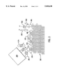
- FIG. 3 illustrates the mechanism as it is believed to occur.
- Crystalline sample structure such as metallic aluminum, is shown at 300.
- Molecules of 1,2 di-iodo-ethane are shown at 305, 310, 315 being directed from an injection needle 320.
- Molecules of 1,2 di-iodo-ethane 325, 330, 335, 340 are shown as building up a concentration on the upper surface of the sample. No measurable chemical reaction was found to take place on the surface from the simple exposure of 1,2 di-iodo-ethane.
- the 1,2 di-iodo-ethane surface layer is altered and a chemical change occurs which lowers the surface binding energy.
- Atoms of the crystalline metal are removed in molecules 355, 360, 365.
- the physics of sputtering is such that it is limited both by the kinetic energy transport within the solid or liquid sample and the binding energy of the surface atoms/molecules.
- the impinging ion mass or type only influences the sputtering rate insofar as it relates to energy transfer.
- the role the primary ions play in relation to the enhanced etching relates to activation of the 1,2 di-iodo-ethane--it is believed that free iodine atoms or ions bind to the aluminum or other sample material and lower the surface binding energy so that physical sputtering is accelerated and therefore etching rates are increased.
- the acceleration can be at least 15 ⁇ . Dielectric etching is accelerated by a factor of ⁇ 4 ⁇ . Some metals, such as tungsten, do not appear to experience an acceleration of etching rate with 1,2, di-iodo-ethane. As most integrated circuit metallization is now aluminum 1,2 di-iodo-ethane is useful for rapid and preferential etching of aluminum conductors. Because all metals are not accelerated in the same way and as they have differing secondary emission coefficients, care must be taken when etching a metal trace to sever the metallization that the barrier material is removed as well as the aluminum metallization.
- selectivity is of most importance in the etching process. Less operator expertise is required when the process removes metal preferentially relative to dielectric. The process then has more precision and more uniformity.
- 1,2 di-iodo-ethane is not classified as hazardous for shipping. This simplifies handling and shipping. Because of finite shelf life, the 1,2 di-iodo-ethane compound is preferably stored in a sealed plastic storage bag, below 5° Celcius (40° Fahrenheit) in a refrigerator dedicated to chemical storage. The compound 1,2 di-iodo-ethane decomposes with time, and subsequent increased pressure requires a purge routine.
- the crucible Before commencing etching, it is preferable to heat the crucible and flow the 1,2 di-iodo-ethane compound through the tubulation and the injection needle into the vacuum chamber of the FIB system for about 5 minutes.
- This purging is critical because the pre-purged chemical can cause formation on the sample of a compound which is difficult to mill with either the purged chemical or with the unassisted Ga+ focused-ion beam.
- the compound formed on the sample by the pre-purged chemical has been found to be non-uniform, which results during subsequent etching in removal of some dielectric under the aluminum while leaving some of the compound.
- the acceleration factor has been found to be 10 or greater.
- Enhanced FIB etching with 1,2 di-iodo-ethane has a number of advantages:
- the compound 1,2 di-iodo-ethane operates cleaner than iodine.
- 1,2 di-iodo-ethane does not coat the inside of delivery tubing or foul the crucible valves, and is not considered hazardous material for shipping purposes.
- Prior iodine contamination of the system appears to be removed by 1,2 di-iodo-ethane.
- the 5-minute purge sequence for 1,2 di-iodo-ethane (described above) is adequate to stabilize the process, and is of considerably shorter duration than that required for iodine.
- the crucible is preferably thermally well insulated and maintained at a temperature which provides a working chamber pressure of 3-5 ⁇ 10 -5 Torr.
- Other components of the vapor delivery system outlined above are also preferably thermally well insulated, including the manifold and jet assembly, and are maintained at a temperature above the crucible temperature so as to keep 1,2 di-iodo-ethane vapor from condensing out on some cold spot of the delivery system.
- the vapor delivery system components may be maintained, for example, at or about 60° Celcius.
- the elevated crucible temperature increases the vapor pressure of the 1,2 di-iodo-ethane, which flows through the delivery system, only limited by the manifold valve, and onto the sample surface in a region of interest.
- System total chamber pressure should not exceed 6.0 ⁇ 10 -5 Torr, to avoid damage to devices connected to the chamber, including the ion beam column.
- System total chamber pressure should be less than 1.0 ⁇ 10 -5 Torr before starting a gas-assisted operation. Partial pressure of the 1,2 di-iodo-ethane gas must be over 1.0 ⁇ 10 -5 Torr in order to have a significant effect on operation.
- Preferred nominal operating pressure is 4.0 ⁇ 10 -5 Torr which results when the 1,2 di-iodo-ethane crucible temperature is maintained at 35° Celcius, ⁇ 5° Celcius. This results in a gas flow through the needle of approximately 0.9 SCCM (standard cubic centimeters per minute) and a flow rate at the device surface, some 700 microns away from the injection needle of 800 micron diameter, of approximately 3 ⁇ 10 17 molecules/cm 2 /sec.
- Object To cut a 2 ⁇ m ⁇ 5 ⁇ m hole through an aluminum layer. With the chamber pressure initially below 1.0 ⁇ 10 -5 Torr, the 1,2 di-iodo-ethane (held at 35° Celcius) is introduced to the chamber resulting in a chamber pressure of 4.0 ⁇ 10 -5 Torr.
- the ion beam current is determined by requiring a beam current density of at least 10 pA/ ⁇ m 2 , therefore a 100 pA beam is used for this case.
- the beam is then turned on and in approximately 30 seconds the beam will have etched through 1 ⁇ m of aluminum.
- the same size box with the same beam current but without introducing the 1,2 di-iodo-ethane gas to the device surface would take over 15 minutes.
- Object To cut a 2 ⁇ m ⁇ 5 ⁇ m hole through an aluminum layer but with a less than optimal beam current density. If in this example the beam current is chosen to be 20 pA, resulting in 2 pA/ ⁇ m 2 beam current density, then cutting through 1 ⁇ m of aluminum will take a little over 2 minutes as opposed to 30 seconds at 10 pA/ ⁇ m 2 .
- Object To cut a 2 ⁇ m ⁇ 5 ⁇ m hole through an aluminum layer but with a more than optimal beam current density. If in this example the beam current is chosen to be 250 pA, resulting in 25 pA/ ⁇ m 2 beam current density, then cutting through 1 ⁇ m of aluminum will only take approximately 10 seconds. While this is faster than 30 seconds, the high milling rate makes it more difficult for the operator or the machine to stop after going through the aluminum and the higher beam current density will also start cutting through what is beneath the aluminum more quickly, resulting in a less precise operation.
- FIB etching enhanced with 1,2 di-iodo-ethane gas has been tested on gold thin-films and found to result in an etch rate enhancement (compared to the etch rate without using any gas at all) of some 5 to 7 times. It performs in a similar manner to etching aluminum but with less than half the etching enhancement Acceleration Factor. This can still be a useful tool for repairing x-ray lithography masks and high-power GaAs and Si devices as well as other processes that use gold thin-films.
- a FIB system suitable for carrying out the methods of the present invention is the IDS P2X system, available commercially from Schlumberger Technologies, Inc., of San Jose, Calif.
- chamber pressures were monitored using the Penning gauge of the IDS P2X system. Since the gas flux and pressure at the surface of the DUT were not measured, the calibration data and chamber pressures were used as an indirect indicator.
- Etching is conducted by scanning the FIB over a specified "box" (e.g. a region of 2 ⁇ m ⁇ 5 ⁇ m or other specified dimension) while vapor is injected at the surface of the region through a needle. Regardless of the box dimension, 500 horizontal scan lines are used to cover the region, and one full sweep of the box is performed in 30 milliseconds (ms).
- a specified "box” e.g. a region of 2 ⁇ m ⁇ 5 ⁇ m or other specified dimension
- Table 1 is a summary of useful ranges and optimum/typical values for FIB etching of aluminum enhanced with injection of 1,2 di-iodo-ethane.
- FIG. 5 shows an approximate relationship between milling acceleration and ion current when etching aluminum in accordance with the invention.
- the ion current is given for a nominal FIB working area size of about 4 ⁇ m 2 .
Landscapes
- Engineering & Computer Science (AREA)
- Chemical & Material Sciences (AREA)
- General Physics & Mathematics (AREA)
- Manufacturing & Machinery (AREA)
- Metallurgy (AREA)
- Organic Chemistry (AREA)
- Physics & Mathematics (AREA)
- Condensed Matter Physics & Semiconductors (AREA)
- Materials Engineering (AREA)
- Mechanical Engineering (AREA)
- Computer Hardware Design (AREA)
- Microelectronics & Electronic Packaging (AREA)
- Power Engineering (AREA)
- Drying Of Semiconductors (AREA)
- ing And Chemical Polishing (AREA)
- Sampling And Sample Adjustment (AREA)
Abstract
Description
AF=5×T1/T2
              TABLE 1
______________________________________
Parameter    Range of Values
                          Optimum/Typical Value
______________________________________
Average      i-60 pA/μm.sup.2
                          5-10 pA/μm.sup.2
Beam-Current Density
Background   <1.5 × 10.sup.-5 Torr
                          <1.0 × 10.sup.-5 Torr
Chamber Pressure
Total Chamber Pressure
             <6 × 10.sup.-5 Torr
                          4 × 10.sup.-5 to 5 × 10.sup.-5
                          Torr
with 1,2 di-iodo-ethane
Crucible Temperature
             30°-38° Celcius
                          32°-35° Celcius
Injector Temperature
             ˜60° Celcius
                          ˜60° Celcius
Calculated Gas Flux
Milling Rate 0.03-0.6     0.3 μm.sup.3 /second
             μm.sup.3 /second
______________________________________
 Notes to Table I:
 Milling over a region of 2 μm × 2 μm = 4 μm.sup.2, with
 beam currents of 250 pA, 500 pA and 1000 pA, the acceleration factor for
 aluminum removal has been found to be ≈4× at a beam current
 density of 60 pA/μm.sup.2 and to approach unity (1×) at beam
 current densities >60 pA/μm.sup.2. The absolute rate of etching at bea
 current densities ≧60 pA/μm.sup.2 is high, and the low
 acceleration factor means that the the etching process is not as selectiv
 - aluminum and dielectric are both removed at an undesirably high rate fo
 most semiconductor integrated circuit operations.
 No enhancement of aluminum etch rate was noted at a Total Chamber Pressur
 with 1,2 diiodo-ethane of less than about 1.5 × 10.sup.-5 Torr.
 In the Schlumberger IDS P2X system, the practical upper limit of Total
 Chamber Pressure with 1,2 diiodo-ethane is ≈6 × 10.sup.-5
 Torr because, above that value, the 1,2 diiodo-ethane vapor migrates into
 the FIB column and hampers FIB column operation or triggers safety
 interlocks which shut down the FIB column.
 Indicated Crucible Temperature values may vary from machine to machine.
 The Crucible Temperature setting is established to attain the desired
 chamber pressure. Experience has shown that the indicated Total Chamber
 Pressure values are attained with Crucible Temperature settings in the
 indicated ranges.
Claims (16)
Priority Applications (6)
| Application Number | Priority Date | Filing Date | Title |
|---|---|---|---|
| US08/771,804 US5840630A (en) | 1996-12-20 | 1996-12-20 | FBI etching enhanced with 1,2 di-iodo-ethane |
| TW086116824A TW375761B (en) | 1996-12-20 | 1997-11-11 | FIB etching enhanced with 1,2-di-iodo-ethane |
| EP97402995A EP0855734B1 (en) | 1996-12-20 | 1997-12-10 | Method of focused ion beam etching (FIB) enhanced with 1,2-diiodoethane |
| DE69703611T DE69703611T2 (en) | 1996-12-20 | 1997-12-10 | Etching process using a focused ion beam (FIB) with 1,2-diiodoethane |
| JP9345286A JPH10204660A (en) | 1996-12-20 | 1997-12-15 | Focused ion beam etching improved by 1,2-diiodoethane |
| KR1019970070005A KR100510431B1 (en) | 1996-12-20 | 1997-12-17 | F I B etching enhanced with 1,2 de-iodo-ethane |
Applications Claiming Priority (1)
| Application Number | Priority Date | Filing Date | Title |
|---|---|---|---|
| US08/771,804 US5840630A (en) | 1996-12-20 | 1996-12-20 | FBI etching enhanced with 1,2 di-iodo-ethane |
Publications (1)
| Publication Number | Publication Date |
|---|---|
| US5840630A true US5840630A (en) | 1998-11-24 |
Family
ID=25093016
Family Applications (1)
| Application Number | Title | Priority Date | Filing Date |
|---|---|---|---|
| US08/771,804 Expired - Fee Related US5840630A (en) | 1996-12-20 | 1996-12-20 | FBI etching enhanced with 1,2 di-iodo-ethane |
Country Status (6)
| Country | Link |
|---|---|
| US (1) | US5840630A (en) |
| EP (1) | EP0855734B1 (en) |
| JP (1) | JPH10204660A (en) |
| KR (1) | KR100510431B1 (en) |
| DE (1) | DE69703611T2 (en) |
| TW (1) | TW375761B (en) |
Cited By (15)
| Publication number | Priority date | Publication date | Assignee | Title |
|---|---|---|---|---|
| US6211527B1 (en) | 1998-10-09 | 2001-04-03 | Fei Company | Method for device editing |
| US6300628B1 (en) * | 1997-12-11 | 2001-10-09 | Seiko Instruments Inc. | Focused ion beam machining method and device thereof |
| US6365905B1 (en) * | 1998-06-03 | 2002-04-02 | Seiko Instruments Inc. | Focused ion beam processing apparatus |
| US6651313B1 (en) * | 2000-10-06 | 2003-11-25 | International Business Machines Corporation | Method for manufacturing a magnetic head |
| US6730237B2 (en) * | 2001-06-22 | 2004-05-04 | International Business Machines Corporation | Focused ion beam process for removal of copper |
| US6824655B2 (en) | 2001-08-27 | 2004-11-30 | Credence Systems Corporation | Process for charged particle beam micro-machining of copper |
| US6855622B2 (en) | 2002-05-30 | 2005-02-15 | Nptest, Llc | Method and apparatus for forming a cavity in a semiconductor substrate using a charged particle beam |
| US20050072756A1 (en) * | 2003-10-03 | 2005-04-07 | Makarov Vladimir V. | FIB milling of copper over organic dielectrics |
| US6955930B2 (en) | 2002-05-30 | 2005-10-18 | Credence Systems Corporation | Method for determining thickness of a semiconductor substrate at the floor of a trench |
| US7029595B1 (en) * | 2002-08-21 | 2006-04-18 | Advanced Micro Devices, Inc. | Selective etch for uniform metal trace exposure and milling using focused ion beam system |
| US20060097186A1 (en) * | 2003-12-08 | 2006-05-11 | Hitachi High-Technologies | Liquid metal ion gun |
| US20100264111A1 (en) * | 2009-04-17 | 2010-10-21 | Makarov Vladimir V | Enhanced Focused Ion Beam Etching of Dielectrics and Silicon |
| US20190074184A1 (en) * | 2017-07-25 | 2019-03-07 | Tescan Brno, S.R.O. | Method for Removal of Matter |
| US11090434B2 (en) | 2015-11-24 | 2021-08-17 | Insulet Corporation | Automated drug delivery system |
| US20220223431A1 (en) * | 2020-12-28 | 2022-07-14 | American Air Liquide, Inc. | High conductive passivation layers and method of forming the same during high aspect ratio plasma etching |
Families Citing this family (1)
| Publication number | Priority date | Publication date | Assignee | Title |
|---|---|---|---|---|
| KR100590575B1 (en) * | 2004-12-24 | 2006-06-19 | 삼성전자주식회사 | Method of electron beam lithography using new material |
Citations (5)
| Publication number | Priority date | Publication date | Assignee | Title |
|---|---|---|---|---|
| US4226666A (en) * | 1978-08-21 | 1980-10-07 | International Business Machines Corporation | Etching method employing radiation and noble gas halide |
| US5009743A (en) * | 1989-11-06 | 1991-04-23 | Gatan Incorporated | Chemically-assisted ion beam milling system for the preparation of transmission electron microscope specimens |
| US5104164A (en) * | 1989-06-15 | 1992-04-14 | Dom-Sicherheitstechnik Gmbh & Co. Kg | Lock with facility for preventing unauthorized entry |
| US5188705A (en) * | 1991-04-15 | 1993-02-23 | Fei Company | Method of semiconductor device manufacture |
| US5376791A (en) * | 1991-04-15 | 1994-12-27 | Fei Company | Secondary ion mass spectometry system |
Family Cites Families (7)
| Publication number | Priority date | Publication date | Assignee | Title |
|---|---|---|---|---|
| US4126523A (en) * | 1976-10-21 | 1978-11-21 | Alumatec, Inc. | Method and means for electrolytic precleaning of substrates and the electrodeposition of aluminum on said substrates |
| DE3785737T2 (en) * | 1986-12-26 | 1993-09-02 | Seiko Instr Inc | DEVICE FOR REPAIRING A PATTERNED FILM. |
| US4874947A (en) * | 1988-02-26 | 1989-10-17 | Micrion Corporation | Focused ion beam imaging and process control |
| JPH088245B2 (en) * | 1990-09-28 | 1996-01-29 | 株式会社島津製作所 | Focused ion beam etching system |
| US5140164A (en) * | 1991-01-14 | 1992-08-18 | Schlumberger Technologies, Inc. | Ic modification with focused ion beam system |
| DE4421517A1 (en) * | 1993-06-28 | 1995-01-05 | Schlumberger Technologies Inc | Method for removing or depositing material by means of a particle beam and device for carrying out the method |
| US5580419A (en) * | 1994-03-23 | 1996-12-03 | Trw Inc. | Process of making semiconductor device using focused ion beam for resistless in situ etching, deposition, and nucleation |
-
1996
- 1996-12-20 US US08/771,804 patent/US5840630A/en not_active Expired - Fee Related
-
1997
- 1997-11-11 TW TW086116824A patent/TW375761B/en not_active IP Right Cessation
- 1997-12-10 EP EP97402995A patent/EP0855734B1/en not_active Expired - Lifetime
- 1997-12-10 DE DE69703611T patent/DE69703611T2/en not_active Expired - Fee Related
- 1997-12-15 JP JP9345286A patent/JPH10204660A/en active Pending
- 1997-12-17 KR KR1019970070005A patent/KR100510431B1/en not_active IP Right Cessation
Patent Citations (5)
| Publication number | Priority date | Publication date | Assignee | Title |
|---|---|---|---|---|
| US4226666A (en) * | 1978-08-21 | 1980-10-07 | International Business Machines Corporation | Etching method employing radiation and noble gas halide |
| US5104164A (en) * | 1989-06-15 | 1992-04-14 | Dom-Sicherheitstechnik Gmbh & Co. Kg | Lock with facility for preventing unauthorized entry |
| US5009743A (en) * | 1989-11-06 | 1991-04-23 | Gatan Incorporated | Chemically-assisted ion beam milling system for the preparation of transmission electron microscope specimens |
| US5188705A (en) * | 1991-04-15 | 1993-02-23 | Fei Company | Method of semiconductor device manufacture |
| US5376791A (en) * | 1991-04-15 | 1994-12-27 | Fei Company | Secondary ion mass spectometry system |
Non-Patent Citations (6)
| Title |
|---|
| "Dry Etching of III-V Semiconductors in CH3 I, C2 H5 I, and C3 H7 I Discharges"; Chakrabarti et al.; J. Voc. Sci, and Tech, B; vol. 10, No. 6, pp. 2378-2386; Dec. 1992. |
| "Low Temperature Chemically Assisted Ion-Beam Etching Processes Using C1/2, CH3 I, and IBr3 to etch InP Optoelectronic Devices"; J. Voc. Sci. Tech., B (Jun. 1996'), pp. 1780-1783; Eisele et al.; 14(3). |
| Dry Etching of III V Semiconductors in CH 3 I, C 2 H 5 I, and C 3 H 7 I Discharges ; Chakrabarti et al.; J. Voc. Sci, and Tech, B; vol. 10, No. 6, pp. 2378 2386; Dec. 1992. * |
| Low Temperature Chemically Assisted Ion Beam Etching Processes Using C1/2, CH 3 I, and IBr 3 to etch InP Optoelectronic Devices ; J. Voc. Sci. Tech., B (Jun. 1996 ), pp. 1780 1783; Eisele et al.; 14(3). * |
| Materials Safety Data Sheet, Epigrade EDI10 Source for Etching, NovaMOS Division, Advanced Technology Materials, Inc., dated Mar. 27, 1996, four pages. * |
| Materials Safety Data Sheet, Epigrade® EDI10 Source for Etching, NovaMOS Division, Advanced Technology Materials, Inc., dated Mar. 27, 1996, four pages. |
Cited By (29)
| Publication number | Priority date | Publication date | Assignee | Title |
|---|---|---|---|---|
| US6300628B1 (en) * | 1997-12-11 | 2001-10-09 | Seiko Instruments Inc. | Focused ion beam machining method and device thereof |
| US6365905B1 (en) * | 1998-06-03 | 2002-04-02 | Seiko Instruments Inc. | Focused ion beam processing apparatus |
| US6211527B1 (en) | 1998-10-09 | 2001-04-03 | Fei Company | Method for device editing |
| US6268608B1 (en) | 1998-10-09 | 2001-07-31 | Fei Company | Method and apparatus for selective in-situ etching of inter dielectric layers |
| US6651313B1 (en) * | 2000-10-06 | 2003-11-25 | International Business Machines Corporation | Method for manufacturing a magnetic head |
| US7259934B2 (en) * | 2000-10-06 | 2007-08-21 | International Business Machines Corporation | Pole tip trimmed magnetic recording head with minimal edge rounding |
| US20050073775A1 (en) * | 2000-10-06 | 2005-04-07 | Chang Thomas Young | Pole tip trimmed magnetic recording head with minimal edge rounding |
| US6730237B2 (en) * | 2001-06-22 | 2004-05-04 | International Business Machines Corporation | Focused ion beam process for removal of copper |
| US6824655B2 (en) | 2001-08-27 | 2004-11-30 | Credence Systems Corporation | Process for charged particle beam micro-machining of copper |
| US6855622B2 (en) | 2002-05-30 | 2005-02-15 | Nptest, Llc | Method and apparatus for forming a cavity in a semiconductor substrate using a charged particle beam |
| US6955930B2 (en) | 2002-05-30 | 2005-10-18 | Credence Systems Corporation | Method for determining thickness of a semiconductor substrate at the floor of a trench |
| US7029595B1 (en) * | 2002-08-21 | 2006-04-18 | Advanced Micro Devices, Inc. | Selective etch for uniform metal trace exposure and milling using focused ion beam system |
| US20060219949A1 (en) * | 2003-10-03 | 2006-10-05 | Credence Systems Corporation | Fib milling of copper over organic dielectrics |
| US7883630B2 (en) | 2003-10-03 | 2011-02-08 | Dcg Systems, Inc. | FIB milling of copper over organic dielectrics |
| US20050072756A1 (en) * | 2003-10-03 | 2005-04-07 | Makarov Vladimir V. | FIB milling of copper over organic dielectrics |
| US20090114851A1 (en) * | 2003-10-03 | 2009-05-07 | Makarov Vladimir V | Fib milling of copper over organic dielectrics |
| US7060196B2 (en) | 2003-10-03 | 2006-06-13 | Credence Systems Corporation | FIB milling of copper over organic dielectrics |
| US20060097186A1 (en) * | 2003-12-08 | 2006-05-11 | Hitachi High-Technologies | Liquid metal ion gun |
| US7211805B2 (en) * | 2003-12-08 | 2007-05-01 | Hitachi High-Technologies Corporation | Liquid metal ion gun |
| US7420181B2 (en) | 2003-12-08 | 2008-09-02 | Hitachi High-Technologies Corporation | Liquid metal ion gun |
| US20080210883A1 (en) * | 2003-12-08 | 2008-09-04 | Hitachi High-Technologies Corporation | Liquid metal ion gun |
| US7804073B2 (en) | 2003-12-08 | 2010-09-28 | Hitachi High-Technologies Corporation | Liquid metal ion gun |
| US20100264111A1 (en) * | 2009-04-17 | 2010-10-21 | Makarov Vladimir V | Enhanced Focused Ion Beam Etching of Dielectrics and Silicon |
| US8277672B2 (en) | 2009-04-17 | 2012-10-02 | Tiza Lab, LLC | Enhanced focused ion beam etching of dielectrics and silicon |
| US11090434B2 (en) | 2015-11-24 | 2021-08-17 | Insulet Corporation | Automated drug delivery system |
| US11744944B2 (en) | 2015-11-24 | 2023-09-05 | Insulet Corporation | Wearable automated medication delivery system |
| US20190074184A1 (en) * | 2017-07-25 | 2019-03-07 | Tescan Brno, S.R.O. | Method for Removal of Matter |
| US10832918B2 (en) * | 2017-07-25 | 2020-11-10 | Tescan Brno, S.R.O. | Method for removal of matter |
| US20220223431A1 (en) * | 2020-12-28 | 2022-07-14 | American Air Liquide, Inc. | High conductive passivation layers and method of forming the same during high aspect ratio plasma etching |
Also Published As
| Publication number | Publication date |
|---|---|
| KR19980064271A (en) | 1998-10-07 |
| DE69703611D1 (en) | 2001-01-04 |
| TW375761B (en) | 1999-12-01 |
| KR100510431B1 (en) | 2005-11-11 |
| EP0855734A1 (en) | 1998-07-29 |
| JPH10204660A (en) | 1998-08-04 |
| EP0855734B1 (en) | 2000-11-29 |
| DE69703611T2 (en) | 2001-05-03 |
Similar Documents
| Publication | Publication Date | Title |
|---|---|---|
| US5840630A (en) | FBI etching enhanced with 1,2 di-iodo-ethane | |
| US6926935B2 (en) | Proximity deposition | |
| US10304658B2 (en) | Electron beam-induced etching | |
| US6268608B1 (en) | Method and apparatus for selective in-situ etching of inter dielectric layers | |
| Joyce et al. | An investigation of silicon-oxygen interactions using Auger electron spectroscopy | |
| US8921811B2 (en) | High pressure charged particle beam system | |
| US7883630B2 (en) | FIB milling of copper over organic dielectrics | |
| US6730237B2 (en) | Focused ion beam process for removal of copper | |
| JP2003504616A (en) | Method and apparatus for increasing the yield of secondary ions | |
| US9799490B2 (en) | Charged particle beam processing using process gas and cooled surface | |
| Lipp et al. | A comparison of focused ion beam and electron beam induced deposition processes | |
| US10103008B2 (en) | Charged particle beam-induced etching | |
| EP1048071B1 (en) | Integrated circuit rewiring using gas-assisted focused ion beam (fib) etching | |
| US20040262518A1 (en) | Metrology process for enhancing image contrast | |
| TWI730407B (en) | Ion implantation processes and apparatus using gallium | |
| US20040132287A1 (en) | Dry etch process for copper | |
| Park et al. | Comparison of beam-induced deposition using ion microprobe | |
| US20240030004A1 (en) | Ion beam irradiation apparatus and method | |
| Sahra Gard | Construction and testing of a hydrogen cracking cell | |
| Durandet et al. | Pure silicon plasma in a helicon plasma deposition system | |
| JPH08129981A (en) | Field emission type electron gun and electron beam device | |
| Brooks et al. | Lithium-argon discharges in a multicusp-ECR microwave resonant cavity | |
| Chiang | Surface kinetic study of ion induced chemical vapor deposition of copper | |
| Ross | Nano-cellular microstructure evolution in ion-induced chemical vapor deposition (II-CVD) of copper | |
| JPS61242990A (en) | Particle beam source for particle beam epitaxial apparatus |
Legal Events
| Date | Code | Title | Description |
|---|---|---|---|
| AS | Assignment |
Owner name: SCHLUMBERGER TECHNOLOGIES, INC., CALIFORNIA Free format text: ASSIGNMENT OF ASSIGNORS INTEREST;ASSIGNORS:CECERE, MICHAEL A.;LUNDQUIST, THEODORE RALPH;REEL/FRAME:008476/0355 Effective date: 19970306 |
|
| FEPP | Fee payment procedure |
Free format text: PAYOR NUMBER ASSIGNED (ORIGINAL EVENT CODE: ASPN); ENTITY STATUS OF PATENT OWNER: SMALL ENTITY |
|
| CC | Certificate of correction | ||
| FPAY | Fee payment |
Year of fee payment: 4 |
|
| AS | Assignment |
Owner name: NPTEST, LLC, CALIFORNIA Free format text: ASSIGNMENT OF ASSIGNORS INTEREST;ASSIGNOR:SCHLUMBERGER TECHNOLOGIES, INC.;REEL/FRAME:014268/0115 Effective date: 20020510 |
|
| AS | Assignment |
Owner name: CREDENCE SYSTEMS CORPORATION, CALIFORNIA Free format text: ASSIGNMENT OF ASSIGNORS INTEREST;ASSIGNOR:NPTEST, LLC;REEL/FRAME:015242/0574 Effective date: 20040713 |
|
| FPAY | Fee payment |
Year of fee payment: 8 |
|
| FEPP | Fee payment procedure |
Free format text: PAT HOLDER CLAIMS SMALL ENTITY STATUS, ENTITY STATUS SET TO SMALL (ORIGINAL EVENT CODE: LTOS); ENTITY STATUS OF PATENT OWNER: SMALL ENTITY |
|
| AS | Assignment |
Owner name: DCG SYSTEMS, INC., CALIFORNIA Free format text: ASSIGNMENT OF ASSIGNORS INTEREST;ASSIGNOR:CREDENCE SYSTEMS CORPORATION;REEL/FRAME:023519/0001 Effective date: 20080220 |
|
| REMI | Maintenance fee reminder mailed | ||
| LAPS | Lapse for failure to pay maintenance fees | ||
| STCH | Information on status: patent discontinuation |
Free format text: PATENT EXPIRED DUE TO NONPAYMENT OF MAINTENANCE FEES UNDER 37 CFR 1.362 |
|
| FP | Lapsed due to failure to pay maintenance fee |
Effective date: 20101124 |