US5822366A - Transceiver and method for generating and processing complex I/Q-signals - Google Patents
Transceiver and method for generating and processing complex I/Q-signals Download PDFInfo
- Publication number
- US5822366A US5822366A US08/634,509 US63450996A US5822366A US 5822366 A US5822366 A US 5822366A US 63450996 A US63450996 A US 63450996A US 5822366 A US5822366 A US 5822366A
- Authority
- US
- United States
- Prior art keywords
- signal
- frequency
- mixer
- reception
- mixing
- Prior art date
- Legal status (The legal status is an assumption and is not a legal conclusion. Google has not performed a legal analysis and makes no representation as to the accuracy of the status listed.)
- Expired - Lifetime
Links
- 238000000034 method Methods 0.000 title claims description 19
- 230000005540 biological transmission Effects 0.000 claims abstract description 58
- 238000002156 mixing Methods 0.000 claims abstract description 41
- 230000010363 phase shift Effects 0.000 claims abstract description 41
- 230000000694 effects Effects 0.000 claims abstract description 11
- 238000010295 mobile communication Methods 0.000 description 6
- 239000013598 vector Substances 0.000 description 5
- 238000006243 chemical reaction Methods 0.000 description 4
- 230000003321 amplification Effects 0.000 description 3
- 230000008878 coupling Effects 0.000 description 3
- 238000010168 coupling process Methods 0.000 description 3
- 238000005859 coupling reaction Methods 0.000 description 3
- 230000001419 dependent effect Effects 0.000 description 3
- 238000001914 filtration Methods 0.000 description 3
- 238000003199 nucleic acid amplification method Methods 0.000 description 3
- 239000004020 conductor Substances 0.000 description 2
- 238000004519 manufacturing process Methods 0.000 description 2
- 238000007792 addition Methods 0.000 description 1
- 230000015572 biosynthetic process Effects 0.000 description 1
- 230000003247 decreasing effect Effects 0.000 description 1
- 230000001934 delay Effects 0.000 description 1
- 238000010586 diagram Methods 0.000 description 1
- 238000002955 isolation Methods 0.000 description 1
- 239000000463 material Substances 0.000 description 1
- 235000014366 other mixer Nutrition 0.000 description 1
- 230000002265 prevention Effects 0.000 description 1
- 238000005070 sampling Methods 0.000 description 1
- 229910052710 silicon Inorganic materials 0.000 description 1
- 239000010703 silicon Substances 0.000 description 1
- 238000003786 synthesis reaction Methods 0.000 description 1
- 230000002194 synthesizing effect Effects 0.000 description 1
Images


Classifications
-
- H—ELECTRICITY
- H03—ELECTRONIC CIRCUITRY
- H03C—MODULATION
- H03C3/00—Angle modulation
- H03C3/02—Details
- H03C3/09—Modifications of modulator for regulating the mean frequency
- H03C3/0908—Modifications of modulator for regulating the mean frequency using a phase locked loop
- H03C3/0975—Modifications of modulator for regulating the mean frequency using a phase locked loop applying frequency modulation in the phase locked loop at components other than the divider, the voltage controlled oscillator or the reference clock
-
- H—ELECTRICITY
- H03—ELECTRONIC CIRCUITRY
- H03C—MODULATION
- H03C3/00—Angle modulation
- H03C3/02—Details
- H03C3/09—Modifications of modulator for regulating the mean frequency
- H03C3/0908—Modifications of modulator for regulating the mean frequency using a phase locked loop
- H03C3/0941—Modifications of modulator for regulating the mean frequency using a phase locked loop applying frequency modulation at more than one point in the loop
-
- H—ELECTRICITY
- H03—ELECTRONIC CIRCUITRY
- H03C—MODULATION
- H03C3/00—Angle modulation
- H03C3/02—Details
- H03C3/09—Modifications of modulator for regulating the mean frequency
- H03C3/0908—Modifications of modulator for regulating the mean frequency using a phase locked loop
- H03C3/0966—Modifications of modulator for regulating the mean frequency using a phase locked loop modulating the reference clock
-
- H—ELECTRICITY
- H03—ELECTRONIC CIRCUITRY
- H03D—DEMODULATION OR TRANSFERENCE OF MODULATION FROM ONE CARRIER TO ANOTHER
- H03D3/00—Demodulation of angle-, frequency- or phase- modulated oscillations
- H03D3/007—Demodulation of angle-, frequency- or phase- modulated oscillations by converting the oscillations into two quadrature related signals
-
- H—ELECTRICITY
- H03—ELECTRONIC CIRCUITRY
- H03D—DEMODULATION OR TRANSFERENCE OF MODULATION FROM ONE CARRIER TO ANOTHER
- H03D7/00—Transference of modulation from one carrier to another, e.g. frequency-changing
- H03D7/16—Multiple-frequency-changing
- H03D7/165—Multiple-frequency-changing at least two frequency changers being located in different paths, e.g. in two paths with carriers in quadrature
-
- H—ELECTRICITY
- H04—ELECTRIC COMMUNICATION TECHNIQUE
- H04B—TRANSMISSION
- H04B1/00—Details of transmission systems, not covered by a single one of groups H04B3/00 - H04B13/00; Details of transmission systems not characterised by the medium used for transmission
- H04B1/06—Receivers
- H04B1/16—Circuits
- H04B1/30—Circuits for homodyne or synchrodyne receivers
-
- H—ELECTRICITY
- H04—ELECTRIC COMMUNICATION TECHNIQUE
- H04L—TRANSMISSION OF DIGITAL INFORMATION, e.g. TELEGRAPHIC COMMUNICATION
- H04L27/00—Modulated-carrier systems
- H04L27/18—Phase-modulated carrier systems, i.e. using phase-shift keying
- H04L27/20—Modulator circuits; Transmitter circuits
-
- H—ELECTRICITY
- H04—ELECTRIC COMMUNICATION TECHNIQUE
- H04L—TRANSMISSION OF DIGITAL INFORMATION, e.g. TELEGRAPHIC COMMUNICATION
- H04L27/00—Modulated-carrier systems
- H04L27/18—Phase-modulated carrier systems, i.e. using phase-shift keying
- H04L27/22—Demodulator circuits; Receiver circuits
- H04L27/227—Demodulator circuits; Receiver circuits using coherent demodulation
- H04L27/2271—Demodulator circuits; Receiver circuits using coherent demodulation wherein the carrier recovery circuit uses only the demodulated signals
- H04L27/2273—Demodulator circuits; Receiver circuits using coherent demodulation wherein the carrier recovery circuit uses only the demodulated signals associated with quadrature demodulation, e.g. Costas loop
-
- H—ELECTRICITY
- H03—ELECTRONIC CIRCUITRY
- H03B—GENERATION OF OSCILLATIONS, DIRECTLY OR BY FREQUENCY-CHANGING, BY CIRCUITS EMPLOYING ACTIVE ELEMENTS WHICH OPERATE IN A NON-SWITCHING MANNER; GENERATION OF NOISE BY SUCH CIRCUITS
- H03B19/00—Generation of oscillations by non-regenerative frequency multiplication or division of a signal from a separate source
-
- H—ELECTRICITY
- H03—ELECTRONIC CIRCUITRY
- H03B—GENERATION OF OSCILLATIONS, DIRECTLY OR BY FREQUENCY-CHANGING, BY CIRCUITS EMPLOYING ACTIVE ELEMENTS WHICH OPERATE IN A NON-SWITCHING MANNER; GENERATION OF NOISE BY SUCH CIRCUITS
- H03B27/00—Generation of oscillations providing a plurality of outputs of the same frequency but differing in phase, other than merely two anti-phase outputs
-
- H—ELECTRICITY
- H04—ELECTRIC COMMUNICATION TECHNIQUE
- H04L—TRANSMISSION OF DIGITAL INFORMATION, e.g. TELEGRAPHIC COMMUNICATION
- H04L27/00—Modulated-carrier systems
- H04L27/0014—Carrier regulation
- H04L2027/0024—Carrier regulation at the receiver end
- H04L2027/0026—Correction of carrier offset
- H04L2027/0028—Correction of carrier offset at passband only
-
- H—ELECTRICITY
- H04—ELECTRIC COMMUNICATION TECHNIQUE
- H04L—TRANSMISSION OF DIGITAL INFORMATION, e.g. TELEGRAPHIC COMMUNICATION
- H04L27/00—Modulated-carrier systems
- H04L27/0014—Carrier regulation
- H04L2027/0044—Control loops for carrier regulation
- H04L2027/0053—Closed loops
- H04L2027/0057—Closed loops quadrature phase
-
- H—ELECTRICITY
- H04—ELECTRIC COMMUNICATION TECHNIQUE
- H04L—TRANSMISSION OF DIGITAL INFORMATION, e.g. TELEGRAPHIC COMMUNICATION
- H04L27/00—Modulated-carrier systems
- H04L27/0014—Carrier regulation
- H04L2027/0044—Control loops for carrier regulation
- H04L2027/0063—Elements of loops
- H04L2027/0067—Phase error detectors
Definitions
- the invention relates to a method and a transceiver for generating a complex I/Q-signal at a transmission frequency and for receiving the same at a reception frequency.
- the object of the invention is a transceiver based on the I/Q architecture.
- I/Q-transceivers are generally used in digital radio-frequency data transmission which is based on phase modulation.
- this kind of a receiver is also linear, meaning that the amplitude of the output signal obtained from the receiver is linearly proportional to the amplitude of an input signal.
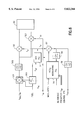
- FIG. 1 shows a known radio-frequency transceiver in which the reception is based on direct conversion.
- received signals coming from antenna 1 are brought, via deplexer 2 separating the transmission and reception signals, to receiver 3, of which only the parts essential to the description of the principle of the invention are presented in FIG. 1.
- the signal received by direct conversion is expressed in the form of zero-frequency I- and Q-vectors of the carrier wave, and is further A/D-converted into digital sampled data I RX (t n ) and Q RX (t n ).
- A(t) is the signal amplitude as a function of time
- ⁇ c is the angular frequency of the carrier wave
- ⁇ (t) is the phase of the carrier wave and, especially in the case of phase modulation, the ⁇ (t) that varies as a function of time represents the modulation.
- the value of the equation (1) at moment t n in time is presented as vector 21 in FIG. 2.
- the reception takes place so that two carriewave frequency ⁇ c signals U I (t) and U Q (t) are formed in the receiver, the one of them, i.e., the I-component, being in the same phase with the unmodulated carrier wave, i.e.:
- phase quadrature component i.e. the phase quadrature component, which is phase-shifted by 90 degrees with the above, is:
- the modulation for the transmission takes place in modulator 4 shown in FIG. 1 so that, in multipliers 5 and 6, the unmodulated I- and Q-components of desired carrierwave frequency ⁇ c are multiplied by modulations I TX (t) and Q TX (t) and summed in adder 7 into a desired modulated transmission signal.
- the requirement of accuracy for the phase difference between the I- and Q-components is in the order of a few degrees.
- the implementation of the I/Q-transceiver is made rather difficult because of the fact that on the circuit board (in the circuit board material) of the transceiver the wavelength of a 1 GHz frequency signal is about 10 cm, whereby a phase shift of tens of degrees occurs in the conductors between the different parts of the transceiver. Furthermore, a phase shift of tens of degrees to the 1 GHz frequency signal easily occurs in the amplifier stages, which phase shift often depends on the temperature, and varies from unit to unit and is therefore difficult to manage. To a 2 GHz frequency the wavelength on the circuit board is only 5 cm and the phase shift in the amplifiers is larger than on the 1 GHz frequency. Therefore, the wiring of the I- and Q-signals or local frequencies U I and U Q from a synthesizer to the multipliers, maintaining the 90° phase shift, is problematic.
- FIG. 3a A known method/device for implementing the 90° phase shift not dependent on the frequency is shown in FIG. 3a, where the input frequency is doubled in a frequency doubler 31, the Q-branch is inverted in an inverting amplifier, such as logic inverter 32, corresponding to a 180° phase shift, and finally, the I- and Q-signals are divided by two in dividers 33 and 34. If the total delays of the I- and Q-branches from point A to points B1 and B2 are equal and the phase shift caused by amplifier 32 is 180°, output signals U I and U Q are in a 90° degree phase shift to one another. This is illustrated in FIG. 3b in which the signals are shown in different points A, B, B', B1, B2 in the circuit of FIG. 3a.
- the circuit of FIG. 3a is functional and can be integrated, but the structures are partially redundant, they consume power and require operation on a double frequency with respect to the RF-frequency of the equipment. Consequently, in radio sets of 1 GHz, for example, the operating frequency of the dividers is 2 GHz and, correspondingly, in devices operating on frequencies of 2 GHz, the circuit would operate on a 4 GHz frequency, causing problems with the silicon in integrated circuits (where such high operating frequencies are difficult to achieve).
- the purpose of the present invention is to eliminate the problems mentioned above.
- the phase difference between the I- and Q-branches on the mixing circuits can be controlled accurately by means of the invention, independent of the phase shifts between the frequency synthesizer and the mixers or the variations thereof so that in order to implement the phase shift, neither double operating frequencies nor phase shifters dependent on the frequency are necessary.
- the invention can be used to eliminate phasing problems of RF-signals generally occurring in I/Q-transceivers, the requirements for accuracy of multipliers used as mixers and modulators are essentially decreased, and the operation of the device is made possible on a wide frequency range and essentially on two different frequency ranges, the other frequencies preferably being about twice as high as the others.
- the above-mentioned objects are achieved by arranging two frequency synthesizers in the transceiver for providing a first mixer signal to mix the input signal of the receiver (called the I-component in the I-branch) into a lower-frequency I-signal, and for providing a second mixer signal to mix the input signal of the receiver (called the Q-signal in the Q-branch) into a lower-frequency Q-signal.
- the accurate 90° degree phase difference of the I- and Q-signals is implemented by adjusting the received I- and Q-signals first to the same phase and, thereafter, by controlling the mixer signals into a 90° degree mutual phase shift. In this way, it is ensured that the I- and Q-signals are in the 90° phase shift with respect to one another.
- the same frequency synthesizers can be further used to provide two different transmission frequencies.
- a higher transmission frequency is formed by mixing said first and second mixer signals, one of which has been modulated to form and provide the sum signal thereof as an output.
- a lower transmission frequency is formed directly from the other mixer signal.
- the transceiver according to the invention can be used to receive two different reception frequencies.
- the higher-frequency reception signal is down-converted by using the first mixer signal into a lower reception frequency while the receiver operates on the higher reception frequency.
- the reception signal is only mixed with a zero-frequency signal, whereby the frequency of the received signal is not altered.
- the transceiver according to the invention for generating complex I/Q-signals on a transmission frequency and for receiving the same on a reception frequency, the receiver comprising:
- the first branch comprises a first mixer for mixing the I-component of the received signal into a lower-frequency I-signal
- the second branch comprises a second mixer for mixing the Q-component of the received signal into a lower-frequency Q-signal
- a first frequency synthesizer for forming a first mixer signal for the mixer of the first branch to mix said I-component into said I-signal
- a second frequency synthesizer for forming a second mixer signal for the mixer of the second branch to mix said Q-component into said Q-signal
- control means first for controlling said first and second mixer signals into the same phase with respect to their mixing effects, and thereafter, into a 90 degree mutual phase shift with respect to their mixing effects when receiving signals in order to bring said lower-frequency I- and Q-signals into the 90 degree mutual phase shift.
- the I-signal is processed in the first branch
- the I-component of the signal received in the first branch is mixed into a lower-frequency I-signal
- the Q-component of the signal received in the second branch is mixed into a lower-frequency Q-signal
- a first frequency synthesizer is used to form a first mixer signal which is used to mix the I-component of the received signal into a lower-frequency I-signal, and
- a second frequency synthesizer is used to form a second mixer signal (f LQ ) which is used to mix the Q-component of the received signal into a lower-frequency Q-signal, and p1 the first and second mixer signals are first controlled into the same phase with respect to their mixing effects, whereby said lower-frequency I-signal and said lower-frequency Q-signal are of the same phase, and
- said mixer signals are controlled into a 90 degree mutual phase shift, whereby said lower-frequency I-signal and said lower-frequency Q-signal are in a 90 degree phase shift with one another.
- FIG. 1 presents the structure of a known prior art transceiver with respect to the modulation
- FIG. 2 presents the vector presentation of the I- and Q-signals
- FIG. 3a presents a known prior art solution for implementing the 90° phase shift
- FIG. 3b presents the stages and phases of signals in different points of the block diagram shown in FIG. 3a
- FIG. 4 presents the transceiver according to the invention in one of its operating modes
- FIG. 5 presents a PLL synthesizer circuit
- FIG. 6 presents the transceiver according to the invention in another operating mode
- FIG. 7 presents an example of the transmission and reception frequency ranges of a mobile phone system operating in two different frequency ranges
- FIG. 8 presents the synthesizer frequencies used in the invention for different mobile communication systems.
- the frequency-generation of the transceiver according to the invention for one transmission and reception frequency range is presented in FIG. 4. It is assumed, for exemplary purposes, that transmission frequency f TX is 890 MHz and reception frequency f RX is 935 MHz (which is the lowest frequency of the reception range in the GSM mobile communication system), and that transmission does not occur simultaneously with reception, i.e., time division multiple access (TDMA) is used, for example, in which the transmission and the reception take place in different time slots.
- TDMA time division multiple access
- the receiver operates according to the direct conversion principle, i.e., the modulation on an RF frequency is converted directly into base-band frequency I- and Q-vectors.
- the direct conversion of the received signal is presented in, e.g., publication EP 346 986.
- the lower-frequency I-component of input signal f RX is obtained by mixing it in mixer 42 with local signal f LI obtained from the output of oscillator 41 operating on reception frequency f RX , and by filtering the outputs obtained from mixer 42 by using filter 43 (such as a lowpass filter).
- filter 43 such as a lowpass filter
- the signal of the Q-branch is mixed in second mixer 421 into a lower frequency, and the desired frequency is filtered from the mixing results in second filter 431 (such as a lowpass filter).
- Reception signal f RX and unmodulated local frequency f LQ which is approximately of the same frequency with it, are conducted as input signals to mixer 421, the f LQ being of the same frequency as local signal f LI of the I-branch but in a 90 degree phase shift with respect to the same.
- the I- and Q-signals are further converted into digital words at sampling frequency f S in A/D-converters 44 and 441 and processed in signal processor 45 whose functions related to the invention are described below.
- Local frequency f LQ is generated according to the invention in the reception state so that the output signal of oscillator 411 is led to input 461 of synthesizer circuit 46, the phase difference from the synthesizer circuit being filtered in loop filter 49 into a control signal of voltage-controlled oscillator 411.
- Loop filter 49 generally comprises an integrator and a lowpass filter for integrating and filtering the phase difference.
- Input 462 of synthesizer circuit 46 is not operative in this stage.
- Synthesizer circuit 46 is capable of accurately forming, in addition to the desired frequency, a desired phase and modulation. Solutions related to modulating frequency synthesis and modulation at an offset frequency are described in detail in U.S. Pat. Nos. 5,079,520 and 5,325,075.
- the other internal parts of the synthesizer, pre-scaler 71, divider 72 of the VCO-branch, modulus controller 73 of the pre-scaler, phase comparator 74 and divider 75 of reference frequency f ref are similar to those in the known PLL frequency synthesizer.
- the modulation is applied directly as phase ⁇ to the Modulation input of PLL synthesizer circuit 46, whereby separate I and Q amplitude modulators with respective RF-adders (e.g., 5, 6, and 7 in FIG. 1) are not needed.
- the different parts of the synthesizer according to FIG. 5 already operate with preset parameters according to whether the input signal of synthesizer circuit 46 is a radio-frequency signal to input 461 or an offset frequency signal to input 462.
- the operation of the transceiver shown in FIG. 4 starts by both oscillators 41 and 411 being started and, by using a known method, being directed to search for a signal on the command channels of the mobile communications system.
- the phase difference of local frequencies f LQ and f LI is controlled by synthesizer 46 until the signals of the I- and Q-branches are observed by signal processor 45 to be of the same phase.
- Signal processor 45 receives the I- and Q-signals converted in A/D-converters 44 and 441 and initially sets them in the same phase on the basis of samples I(tn) and Q(tn) obtained from the A/D-converters.
- phase difference ⁇ k of local signals f LI and f LQ is modified stepwise and correlation over N samples between the I- and Q-signals is calculated for each phase difference ⁇ k through the sample to formula: ##EQU3## so that the amount of samples is large enough with respect to the variation of the received signal.
- the phase difference ⁇ k which provides the highest value for correlation c( ⁇ k ) thus corresponds to the I- and Q-signals of the same phase, and the following equation is true between them:
- coefficient k is now known, it can be taken into account in signal processing 45.
- the mutual phase of oscillators 41 and 411 is modified with the aid of the 90° synthesizer circuit 46 by using, e.g., an advantageous interpolation method which is described in patent publication U.S. Pat. No. 5,079,520, whereby the I- and Q-signals are set in a 90° phase shift.
- the 90° phase shift is obtained by bringing a control signal to PLL synthesizer circuit 46 from signal processor 45 via controller 40.
- the receiver operation is initiated in the manner required for each respective mobile communications system.
- the phase difference set for oscillators 41 and 411 thus remains unaltered henceforth because the synthesizing with synthesizer 46 takes place according to the phase locking principle and oscillators 41, 411 are locked in the same reference frequency.
- the above-describe method (in the reception) and the coupling presented in FIG. 4 are preferable because, e.g., there is no need to recognize and, thereby, to measure or compensate during the manufacture or the operation of the receiver, the difference in amplification and the phase shifts between the I- and Q-signal paths of the RF-signals occurring in the oscillators, mixers, or the couplings between them.
- synthesizer circuit 46 the control command is provided by signal processor 45 via controller 40
- QPSK-type Quadrature Phase Shift Keying
- phase modulation is implemented in synthesizer circuit 46 in accordance with the above-mentioned patent publications and FIG. 5.
- the method and circuit according to the invention can be used to achieve the advantage, for instance, that mixers 5, 6 and adders 7 shown in FIG. 1, or any compensation of phase shift or that of amplitude deviations are not needed to generate phase-modulated transmission signal f TX .
- the method described above also makes it easy to implement a transceiver operating on a frequency (output/reception frequency) higher than VCO frequencies f LI , f LQ (41, 411, FIG. 4), or essentially on two different frequencies, of which the one is essentially a VCO frequency and the other one is essentially sum f LI +f LQ of the VCO frequencies.
- This kind of hardware architecture is presented in FIG. 6 in such a way that the above-described receiver structures and method are included in block 50 (area marked by the dashed lines in FIG. 4).
- Synthesizer block 51 corresponds to unmodulated synthesizer 41 and block 56 corresponds to the modulating synthesizer that comprises blocks 46, 411, and 49 in FIG.
- the transceiver shown in FIG. 6 can be used (on a higher and a lower frequency range) in two mobile communications systems operating on different frequencies.
- the lower reception frequency is denoted as f RX
- the lower transmission frequency as f TX
- the higher reception frequency as f RXU
- the higher transmission frequency as F TXU .
- reception facility synthesizers 51, 56 operate in a corresponding way to that in the case presented in FIG. 4.
- local frequency f LI is taken to multiplier 501 as the second input signal
- the local-frequency mixing result is taken from the output of the multiplier to filter 502 (such as a bandpass filter) whose center frequency is approximately the same as the lower reception frequency f RX and, due to the manner of mixing, the following equation is valid in the upper reception frequency:
- element 503 When operating on the upper reception frequency f RXU , element 503 (which can be a controllable switch, such as a transistor) selects, on the basis of selection signal FSEL of frequencies, frequency f LI as the second input signal of multiplier 501, and when operating on lower reception frequency f RX , member 503 sets a zero-frequency component for the second input of multiplier 501, whereby multiplier 501 only functions as the amplifier of the lower-frequency signal f RX .
- Control signal FSEL can also be used to control the operation of multiplier 501 so that the amplification, bandwidth, noise and power consumption of the transceiver correspond to the values required on the respective reception frequencies f RX and F RXU .
- sum f LI +f LQ of the output frequencies of synthesizers 51 and 56 is selected as the transmission signal F TXU from the output signal of mixer 57 by using filter 59, and filter 58 is used to select, from the output signal of mixer 57, difference f LQ -f LI of the frequencies of said synthesizers 51, 56 for modulation into desired transfer frequency f 2 to PLL synthesizer circuit 46 of frequency synthesizer 56, i.e., in the transmission state the frequencies adhere to the following group of equations:
- synthesizers 51, 56, mixer 57, and filter 58 of FIG. 6 operate in a corresponding way to that described above on the corresponding blocks in connection with FIG. 4.
- the reception frequency range of subscriber devices is 1930-1990 MHz and the transmission frequency range is 1850-1910 MHz.
- the solution according to FIG. 6 is advantageous when implementing an I/Q-transceiver device operating on high frequencies because in order to implement reception, only the first mixer 501 of the receiver and, in order to implement the transmission to generate modulated transmission signal F TXU , the transfer frequency mixer 57 and filter 59 must be capable of operating on high frequencies.
- This is a great advantage for devices operating on 2 GHz frequency ranges, as well as the fact that, provided with only minor additions, the device is capable of operating on two different frequency ranges, the higher of which is preferably approximately twofold compared to the lower one.
- this device also comprises the same advantages related to manufacturing as the device in FIG. 4.
- radio sets according to the GSM-standard that operate on a 900 MHz frequency
- radio sets according to the DCS 1800 standard that operate on a 1.8 GHz frequency
- radio sets operating in both systems as well as the advantageous combination of 900 MHz GSM mobile stations and cordless DECT mobile stations operating on 1880-1900 MHz frequencies in one radio set.
- the method and transceiver according to the invention avoid the handling of frequencies which are twice the reception frequency when forming the phase difference of the I- and Q-signals in reception, so the desired 90° phase difference is obtained accurately.
Landscapes
- Engineering & Computer Science (AREA)
- Computer Networks & Wireless Communication (AREA)
- Signal Processing (AREA)
- Power Engineering (AREA)
- Transceivers (AREA)
Abstract
Description
U.sub.RX (t)=A(t).cos{ω.sub.c t+φ(t)} (1)
U.sub.I (t)=cos(ω.sub.c t) (2)
U.sub.Q (t)=sin(ω.sub.c t). (3)
I(t.sub.n)=A(t.sub.n).cosφ(t.sub.n)
Q(t.sub.n)=A(t.sub.n).sinφ(t.sub.n) (4)
I(t.sub.n)=kQ(t.sub.n) (8)
F.sub.RXU ≈2.f.sub.LI ≈2f.sub.Rx. (9)
|f.sub.LQ -f.sub.LI |=f.sub.2
f.sub.LI +f.sub.LQ =f.sub.TXU (10)
f.sub.LI (51):829-866,5 MHz
f.sub.LQ (511):881-918,5 MHz
f.sub.LI (51):899-929 MHz
f.sub.LQ (511):951-981 MHz
f.sub.LI (51):829-866,5 MHz,899-995 MHz
f.sub.LQ (511):881-995 MHz
Claims (15)
Applications Claiming Priority (2)
| Application Number | Priority Date | Filing Date | Title |
|---|---|---|---|
| FI951918 | 1995-04-21 | ||
| FI951918A FI951918A7 (en) | 1995-04-21 | 1995-04-21 | Transceiver device and method for generating and processing complex I/Q signals |
Publications (1)
| Publication Number | Publication Date |
|---|---|
| US5822366A true US5822366A (en) | 1998-10-13 |
Family
ID=8543286
Family Applications (1)
| Application Number | Title | Priority Date | Filing Date |
|---|---|---|---|
| US08/634,509 Expired - Lifetime US5822366A (en) | 1995-04-21 | 1996-04-18 | Transceiver and method for generating and processing complex I/Q-signals |
Country Status (4)
| Country | Link |
|---|---|
| US (1) | US5822366A (en) |
| EP (1) | EP0739090B1 (en) |
| DE (1) | DE69616136T2 (en) |
| FI (1) | FI951918A7 (en) |
Cited By (29)
| Publication number | Priority date | Publication date | Assignee | Title |
|---|---|---|---|---|
| US6085075A (en) * | 1997-12-05 | 2000-07-04 | U.S. Philips Corporation | Communication system, a communication device and a frequency synthesizer |
| US6385443B1 (en) * | 1998-12-17 | 2002-05-07 | Lg Information & Communications, Ltd. | Intermediate frequency local generating circuit |
| US6385276B1 (en) | 2001-06-12 | 2002-05-07 | Rf Micro Devices, Inc. | Dual-modulus prescaler |
| US6411660B1 (en) * | 1997-05-16 | 2002-06-25 | Samsung Electronics, Co., Ltd. | Device for reducing lock-up time of Frequency synthesizer |
| US20020094788A1 (en) * | 2001-01-12 | 2002-07-18 | Hitachi, Ltd. | Signal processing semiconductor integrated circuit device and wireless communication system |
| US20020094792A1 (en) * | 2001-01-12 | 2002-07-18 | Hitachi, Ltd. | Signal processing semiconductor integrated circuit device and wireless communication system |
| US6448831B1 (en) | 2001-06-12 | 2002-09-10 | Rf Micro Devices, Inc. | True single-phase flip-flop |
| DE10112575A1 (en) * | 2001-03-15 | 2002-10-02 | Siemens Ag | Method and device for generating mobile radio signals |
| US6463266B1 (en) * | 1999-08-10 | 2002-10-08 | Broadcom Corporation | Radio frequency control for communications systems |
| US20030031267A1 (en) * | 2001-06-12 | 2003-02-13 | Hietala Alex Wayne | Fractional-N digital modulation with analog IQ interface |
| US20040022178A1 (en) * | 2002-08-05 | 2004-02-05 | Samsung Electronics Co., Ltd. | Radio equipment for compensating transmission signals |
| US6693468B2 (en) | 2001-06-12 | 2004-02-17 | Rf Micro Devices, Inc. | Fractional-N synthesizer with improved noise performance |
| US6779010B2 (en) | 2001-06-12 | 2004-08-17 | Rf Micro Devices, Inc. | Accumulator with programmable full-scale range |
| US6782249B1 (en) * | 2000-11-22 | 2004-08-24 | Intel Corporation | Quadrature signal generation in an integrated direct conversion radio receiver |
| US20040176034A1 (en) * | 2003-02-13 | 2004-09-09 | Hunter Jeffrey K. | Systems and methods for reducing radio receiver interference from an on-board avionics transmitter |
| US20040229574A1 (en) * | 2003-04-16 | 2004-11-18 | Peter Pfann | Integrated transceiver circuit with low interference production and sensitivity |
| US20060009971A1 (en) * | 2004-06-30 | 2006-01-12 | Kushner William M | Method and apparatus for characterizing inhalation noise and calculating parameters based on the characterization |
| US20060009970A1 (en) * | 2004-06-30 | 2006-01-12 | Harton Sara M | Method for detecting and attenuating inhalation noise in a communication system |
| US20060020451A1 (en) * | 2004-06-30 | 2006-01-26 | Kushner William M | Method and apparatus for equalizing a speech signal generated within a pressurized air delivery system |
| US20060227898A1 (en) * | 2003-07-10 | 2006-10-12 | Gibson Timothy P | Radio receiver |
| US20070058754A1 (en) * | 2005-09-15 | 2007-03-15 | Ying-Yao Lin | Apparatus and Method for Calibrating IQ Mismatch |
| US20080084861A1 (en) * | 2006-10-10 | 2008-04-10 | Honeywell International Inc. | Avionics communication system and method utilizing multi-channel radio technology and a shared data bus |
| WO2008036389A3 (en) * | 2006-09-21 | 2008-06-26 | Gct Semiconductor Inc | Frequency synthesizer using two phase locked loops |
| US20090017777A1 (en) * | 2007-07-13 | 2009-01-15 | Honeywell International Inc. | Reconfigurable aircraft radio communications system |
| US20090135781A1 (en) * | 1998-11-26 | 2009-05-28 | Nokia Corporation | Method and arrangement for transmitting and receiving rf signals through various radio interfaces of communication systems |
| US20090298451A1 (en) * | 2008-05-29 | 2009-12-03 | Honeywell International Inc. | Reconfigurable aircraft communications system with integrated avionics communication router and audio management functions |
| US7719457B1 (en) * | 2008-12-18 | 2010-05-18 | Teledyne Cougar, Inc. | Digitally tuned digital radio frequency memory |
| US8711993B2 (en) | 2010-12-10 | 2014-04-29 | Honeywell International Inc. | Wideband multi-channel receiver with fixed-frequency notch filter for interference rejection |
| US8848831B2 (en) * | 2012-09-20 | 2014-09-30 | Lsi Corporation | Direct digital synthesis of quadrature modulated signals |
Families Citing this family (12)
| Publication number | Priority date | Publication date | Assignee | Title |
|---|---|---|---|---|
| GB2320631B (en) | 1996-12-23 | 2001-07-18 | Nokia Mobile Phones Ltd | Radio receiver and radio transmitter |
| US6009317A (en) * | 1997-01-17 | 1999-12-28 | Ericsson Inc. | Method and apparatus for compensating for imbalances between quadrature signals |
| SE508290C2 (en) * | 1997-01-21 | 1998-09-21 | Ericsson Telefon Ab L M | Receiver device for two frequency bands |
| US6356736B2 (en) * | 1997-02-28 | 2002-03-12 | Maxim Integrated Products, Inc. | Direct-conversion tuner integrated circuit for direct broadcast satellite television |
| DE59811085D1 (en) * | 1997-09-11 | 2004-05-06 | Infineon Technologies Ag | Oscillator circuitry |
| WO1999062199A1 (en) * | 1998-05-27 | 1999-12-02 | Nokia Corporation | A receiver and receiving method for wireless communication |
| EP0969602B1 (en) * | 1998-07-03 | 2006-12-27 | Sony Deutschland GmbH | Dual band transceiver |
| GB2344948B (en) * | 1998-12-18 | 2002-10-02 | Nokia Mobile Phones Ltd | A transceiver |
| US6560297B1 (en) * | 1999-06-03 | 2003-05-06 | Analog Devices, Inc. | Image rejection downconverter for a translation loop modulator |
| DE10142248A1 (en) * | 2001-08-29 | 2003-01-30 | Infineon Technologies Ag | Transmission arrangement, in particular for mobile radio |
| DE10317600B4 (en) * | 2003-04-16 | 2007-10-25 | Infineon Technologies Ag | Integrated transceiver circuit and compensation method in integrated transceiver circuit |
| SE542226C2 (en) | 2016-07-14 | 2020-03-17 | Icomera Ab | Distributed wireless communication system for moving vehicles |
Citations (12)
| Publication number | Priority date | Publication date | Assignee | Title |
|---|---|---|---|---|
| EP0305603A1 (en) * | 1987-09-03 | 1989-03-08 | Koninklijke Philips Electronics N.V. | Gain and phase correction in a dual branch receiver |
| FI892081A7 (en) * | 1988-05-04 | 1989-11-05 | Alcatel Nv | Quadrature receiver |
| US5079520A (en) * | 1990-01-18 | 1992-01-07 | Nokia Mobile Phones Ltd. | Interpolating phase-locked loop frequency synthesizer |
| EP0541305A1 (en) * | 1991-11-05 | 1993-05-12 | Nokia Mobile Phones Ltd. | A method to generate different frequency signals in a digital radio telephone |
| US5249204A (en) * | 1991-08-12 | 1993-09-28 | Motorola, Inc. | Circuit and method for phase error correction in a digital receiver |
| EP0581573A1 (en) * | 1992-07-28 | 1994-02-02 | Nokia Mobile Phones Ltd. | Universal radio telephone |
| US5291474A (en) * | 1989-05-18 | 1994-03-01 | Nokia Mobile Phones Ltd. | Procedure for forming frequencies of a digital radio telephone |
| US5301367A (en) * | 1991-09-04 | 1994-04-05 | Nokia Mobile Phones Ltd. | Direct digital synthesizer for producing a modulated intermediate frequency in a radio apparatus |
| WO1994014247A1 (en) * | 1992-12-07 | 1994-06-23 | Motorola, Inc. | Circuit for generating signals in phase quadrature and associated method therefor |
| US5325075A (en) * | 1991-12-31 | 1994-06-28 | Nokia Mobile Phones Ltd. | Method and circuit arrangement to generate a phase modulated or frequency modulated signal |
| US5390168A (en) * | 1991-09-25 | 1995-02-14 | Nokia Mobile Phones Ltd. | Radio frequency transmission circuit |
| US5511235A (en) * | 1994-05-02 | 1996-04-23 | Motorola, Inc. | Apparatus for detecting a signaling channel during scanning including a controlled frequency converter circuit and a controlled filter bandwidth, and a method therefor |
-
1995
- 1995-04-21 FI FI951918A patent/FI951918A7/en unknown
-
1996
- 1996-04-16 DE DE69616136T patent/DE69616136T2/en not_active Expired - Fee Related
- 1996-04-16 EP EP96105912A patent/EP0739090B1/en not_active Expired - Lifetime
- 1996-04-18 US US08/634,509 patent/US5822366A/en not_active Expired - Lifetime
Patent Citations (14)
| Publication number | Priority date | Publication date | Assignee | Title |
|---|---|---|---|---|
| EP0305603A1 (en) * | 1987-09-03 | 1989-03-08 | Koninklijke Philips Electronics N.V. | Gain and phase correction in a dual branch receiver |
| FI892081A7 (en) * | 1988-05-04 | 1989-11-05 | Alcatel Nv | Quadrature receiver |
| US4955039A (en) * | 1988-05-04 | 1990-09-04 | Alcatel N.V. | Quadrature receiver |
| US5291474A (en) * | 1989-05-18 | 1994-03-01 | Nokia Mobile Phones Ltd. | Procedure for forming frequencies of a digital radio telephone |
| US5079520A (en) * | 1990-01-18 | 1992-01-07 | Nokia Mobile Phones Ltd. | Interpolating phase-locked loop frequency synthesizer |
| US5249204A (en) * | 1991-08-12 | 1993-09-28 | Motorola, Inc. | Circuit and method for phase error correction in a digital receiver |
| US5301367A (en) * | 1991-09-04 | 1994-04-05 | Nokia Mobile Phones Ltd. | Direct digital synthesizer for producing a modulated intermediate frequency in a radio apparatus |
| US5390168A (en) * | 1991-09-25 | 1995-02-14 | Nokia Mobile Phones Ltd. | Radio frequency transmission circuit |
| EP0541305A1 (en) * | 1991-11-05 | 1993-05-12 | Nokia Mobile Phones Ltd. | A method to generate different frequency signals in a digital radio telephone |
| US5325075A (en) * | 1991-12-31 | 1994-06-28 | Nokia Mobile Phones Ltd. | Method and circuit arrangement to generate a phase modulated or frequency modulated signal |
| EP0581573A1 (en) * | 1992-07-28 | 1994-02-02 | Nokia Mobile Phones Ltd. | Universal radio telephone |
| US5471652A (en) * | 1992-07-28 | 1995-11-28 | Nokia Mobile Phones Ltd. | Frequency synthesizer and multiplier circuit arrangement for a radio telephone |
| WO1994014247A1 (en) * | 1992-12-07 | 1994-06-23 | Motorola, Inc. | Circuit for generating signals in phase quadrature and associated method therefor |
| US5511235A (en) * | 1994-05-02 | 1996-04-23 | Motorola, Inc. | Apparatus for detecting a signaling channel during scanning including a controlled frequency converter circuit and a controlled filter bandwidth, and a method therefor |
Cited By (53)
| Publication number | Priority date | Publication date | Assignee | Title |
|---|---|---|---|---|
| US6411660B1 (en) * | 1997-05-16 | 2002-06-25 | Samsung Electronics, Co., Ltd. | Device for reducing lock-up time of Frequency synthesizer |
| US6085075A (en) * | 1997-12-05 | 2000-07-04 | U.S. Philips Corporation | Communication system, a communication device and a frequency synthesizer |
| US8755834B2 (en) | 1998-11-26 | 2014-06-17 | Nokia Corporation | Method and arrangement for transmitting and receiving RF signals through various radio interfaces of communication systems |
| US8838049B1 (en) | 1998-11-26 | 2014-09-16 | Nokia Corporation | Method and arrangement for transmitting and receiving RF signals through various radio interfaces of communication systems |
| US8768408B2 (en) | 1998-11-26 | 2014-07-01 | Nokia Corporation | Method and arrangement for transmitting and receiving RF signals through various radio interfaces of communication systems |
| US20090135781A1 (en) * | 1998-11-26 | 2009-05-28 | Nokia Corporation | Method and arrangement for transmitting and receiving rf signals through various radio interfaces of communication systems |
| US9270301B2 (en) | 1998-11-26 | 2016-02-23 | Nokia Technologies Oy | Method and arrangement for transmitting and receiving RF signals through various radio interfaces of communication systems |
| US6385443B1 (en) * | 1998-12-17 | 2002-05-07 | Lg Information & Communications, Ltd. | Intermediate frequency local generating circuit |
| US6816716B2 (en) * | 1999-08-10 | 2004-11-09 | Broadcom Corporation | Radio frequency control for communication systems |
| US6463266B1 (en) * | 1999-08-10 | 2002-10-08 | Broadcom Corporation | Radio frequency control for communications systems |
| US20030087617A1 (en) * | 1999-08-10 | 2003-05-08 | Aki Shohara | Radio frequency control for communication systems |
| US6782249B1 (en) * | 2000-11-22 | 2004-08-24 | Intel Corporation | Quadrature signal generation in an integrated direct conversion radio receiver |
| US7085587B2 (en) | 2001-01-12 | 2006-08-01 | Renesas Technology Corp. | Signal processing semiconductor integrated circuit device and wireless communication system |
| US20020094792A1 (en) * | 2001-01-12 | 2002-07-18 | Hitachi, Ltd. | Signal processing semiconductor integrated circuit device and wireless communication system |
| US20020094788A1 (en) * | 2001-01-12 | 2002-07-18 | Hitachi, Ltd. | Signal processing semiconductor integrated circuit device and wireless communication system |
| US7359678B2 (en) | 2001-01-12 | 2008-04-15 | Renesas Technology Corp. | Signal processing semiconductor integrated circuit device and wireless communication system |
| US6909882B2 (en) * | 2001-01-12 | 2005-06-21 | Renesas Technology Corp. | Signal processing semiconductor integrated circuit device and wireless communication system |
| US20050186927A1 (en) * | 2001-01-12 | 2005-08-25 | Renesas Technology Corp. | Signal processing semiconductor integrated circuit device and wireless communication system |
| US7251465B2 (en) | 2001-03-15 | 2007-07-31 | Siemens Aktiengesellschaft | Method and apparatus for producing mobile radio signals |
| US20040121744A1 (en) * | 2001-03-15 | 2004-06-24 | Volker Wannenmacher | Method and apparatus for producing mobile radio signals |
| DE10112575A1 (en) * | 2001-03-15 | 2002-10-02 | Siemens Ag | Method and device for generating mobile radio signals |
| US7003049B2 (en) | 2001-06-12 | 2006-02-21 | Rf Micro Devices, Inc. | Fractional-N digital modulation with analog IQ interface |
| US20030031267A1 (en) * | 2001-06-12 | 2003-02-13 | Hietala Alex Wayne | Fractional-N digital modulation with analog IQ interface |
| US6385276B1 (en) | 2001-06-12 | 2002-05-07 | Rf Micro Devices, Inc. | Dual-modulus prescaler |
| US6448831B1 (en) | 2001-06-12 | 2002-09-10 | Rf Micro Devices, Inc. | True single-phase flip-flop |
| US6779010B2 (en) | 2001-06-12 | 2004-08-17 | Rf Micro Devices, Inc. | Accumulator with programmable full-scale range |
| US6693468B2 (en) | 2001-06-12 | 2004-02-17 | Rf Micro Devices, Inc. | Fractional-N synthesizer with improved noise performance |
| US20040022178A1 (en) * | 2002-08-05 | 2004-02-05 | Samsung Electronics Co., Ltd. | Radio equipment for compensating transmission signals |
| US7319724B2 (en) * | 2002-08-05 | 2008-01-15 | Samsung Electronics Co., Ltd. | Radio equipment using image signals for compensating transmission signals |
| KR101058694B1 (en) * | 2002-08-05 | 2011-08-22 | 삼성전자주식회사 | Radio to compensate for transmission signal |
| US7142818B2 (en) * | 2003-02-13 | 2006-11-28 | Honeywell International, Inc. | Systems and methods for reducing radio receiver interference from an on-board avionics transmitter |
| US20040176034A1 (en) * | 2003-02-13 | 2004-09-09 | Hunter Jeffrey K. | Systems and methods for reducing radio receiver interference from an on-board avionics transmitter |
| CN1538628B (en) * | 2003-04-16 | 2011-04-13 | 因芬尼昂技术股份公司 | Circuit of integrated transceiver |
| US20040229574A1 (en) * | 2003-04-16 | 2004-11-18 | Peter Pfann | Integrated transceiver circuit with low interference production and sensitivity |
| US7398074B2 (en) | 2003-04-16 | 2008-07-08 | Infineon Technologies | Integrated transceiver circuit with low interference production and sensitivity |
| US20060227898A1 (en) * | 2003-07-10 | 2006-10-12 | Gibson Timothy P | Radio receiver |
| US20060009971A1 (en) * | 2004-06-30 | 2006-01-12 | Kushner William M | Method and apparatus for characterizing inhalation noise and calculating parameters based on the characterization |
| US20060009970A1 (en) * | 2004-06-30 | 2006-01-12 | Harton Sara M | Method for detecting and attenuating inhalation noise in a communication system |
| US20060020451A1 (en) * | 2004-06-30 | 2006-01-26 | Kushner William M | Method and apparatus for equalizing a speech signal generated within a pressurized air delivery system |
| US7254535B2 (en) | 2004-06-30 | 2007-08-07 | Motorola, Inc. | Method and apparatus for equalizing a speech signal generated within a pressurized air delivery system |
| US7139701B2 (en) | 2004-06-30 | 2006-11-21 | Motorola, Inc. | Method for detecting and attenuating inhalation noise in a communication system |
| US8325794B2 (en) * | 2005-09-15 | 2012-12-04 | Realtek Semiconductor Corp. | Apparatus and method for calibrating IQ mismatch |
| US20070058754A1 (en) * | 2005-09-15 | 2007-03-15 | Ying-Yao Lin | Apparatus and Method for Calibrating IQ Mismatch |
| WO2008036389A3 (en) * | 2006-09-21 | 2008-06-26 | Gct Semiconductor Inc | Frequency synthesizer using two phase locked loops |
| US20080084861A1 (en) * | 2006-10-10 | 2008-04-10 | Honeywell International Inc. | Avionics communication system and method utilizing multi-channel radio technology and a shared data bus |
| US8081933B2 (en) | 2007-07-13 | 2011-12-20 | Honeywell International Inc. | Reconfigurable aircraft radio communications system |
| US20090017777A1 (en) * | 2007-07-13 | 2009-01-15 | Honeywell International Inc. | Reconfigurable aircraft radio communications system |
| US8019338B2 (en) | 2008-05-29 | 2011-09-13 | Honeywell International Inc. | Reconfigurable aircraft communications system with integrated avionics communication router and audio management functions |
| US20090298451A1 (en) * | 2008-05-29 | 2009-12-03 | Honeywell International Inc. | Reconfigurable aircraft communications system with integrated avionics communication router and audio management functions |
| US7719457B1 (en) * | 2008-12-18 | 2010-05-18 | Teledyne Cougar, Inc. | Digitally tuned digital radio frequency memory |
| US8711993B2 (en) | 2010-12-10 | 2014-04-29 | Honeywell International Inc. | Wideband multi-channel receiver with fixed-frequency notch filter for interference rejection |
| US9042502B2 (en) | 2010-12-10 | 2015-05-26 | Honeywell International Inc. | Wideband multi-channel receiver with fixed-frequency notch filter for interference rejection |
| US8848831B2 (en) * | 2012-09-20 | 2014-09-30 | Lsi Corporation | Direct digital synthesis of quadrature modulated signals |
Also Published As
| Publication number | Publication date |
|---|---|
| FI951918A7 (en) | 1996-10-22 |
| EP0739090A1 (en) | 1996-10-23 |
| EP0739090B1 (en) | 2001-10-24 |
| DE69616136T2 (en) | 2002-06-20 |
| DE69616136D1 (en) | 2001-11-29 |
| FI951918A0 (en) | 1995-04-21 |
Similar Documents
| Publication | Publication Date | Title |
|---|---|---|
| US5822366A (en) | Transceiver and method for generating and processing complex I/Q-signals | |
| US5802463A (en) | Apparatus and method for receiving a modulated radio frequency signal by converting the radio frequency signal to a very low intermediate frequency signal | |
| FI100286B (en) | Transmitter / receiver for transmitting and receiving an RF signal in two frequency ranges | |
| CN1071070C (en) | Transmission and reception apparatus having single phase-locked loop and method thereof | |
| JP3200184B2 (en) | Synthesizer for wireless devices | |
| FI112561B (en) | Transmitter / receiver for transmitting and receiving an RF signal in at least two frequency ranges | |
| US6118984A (en) | Dual conversion radio frequency transceiver | |
| US5991605A (en) | Method and circuit for creating a modulated signal in a transceiver | |
| WO1998008300A9 (en) | Apparatus and method for receiving a modulated radio frequency signal | |
| US6028493A (en) | Elimination of bandpass filter after quadrature modulator in modulation synthesizer circuit | |
| EP1103098A1 (en) | Dual-band image rejection mixer | |
| KR20000070843A (en) | Transmitter comprising a vco | |
| US6009313A (en) | Radio Communication device capable of setting a frequency channel with a small frequency step | |
| US6137995A (en) | Circuit and method of generating a phase locked loop signal having an offset reference | |
| JPH0575495A (en) | Mobile communication equipment | |
| US7333554B2 (en) | Communication system with frequency modulation and a single local oscillator | |
| CN101023577A (en) | Digital noise coupling reduction and variable intermediate frequency generation in mixed signal circuits | |
| WO2004002098A1 (en) | Radio communication apparatus | |
| US20050070234A1 (en) | Translational loop RF transmitter architecture for GSM radio | |
| EP1357667B1 (en) | Frequency synthesizer and transceiver including same | |
| JP3825317B2 (en) | FM modulator using both phase-locked loop and quadrature modulator | |
| GB2325362A (en) | Transceiver which uses transmission signal as local oscillator for reception | |
| JPH04274642A (en) | Orthogonal modulation circuit | |
| US8412116B1 (en) | Wireless transceiver | |
| JPH08340363A (en) | Modulation circuit |
Legal Events
| Date | Code | Title | Description |
|---|---|---|---|
| AS | Assignment |
Owner name: NOKIA MOBILE PHONES LTD., FINLAND Free format text: ASSIGNMENT OF ASSIGNORS INTEREST;ASSIGNOR:RAPELI, JUHA;REEL/FRAME:007983/0563 Effective date: 19960325 |
|
| STCF | Information on status: patent grant |
Free format text: PATENTED CASE |
|
| FPAY | Fee payment |
Year of fee payment: 4 |
|
| FPAY | Fee payment |
Year of fee payment: 8 |
|
| AS | Assignment |
Owner name: QUALCOMM INCORPORATED, CALIFORNIA Free format text: ASSIGNMENT OF ASSIGNORS INTEREST;ASSIGNOR:NOKIA CORPORATION;REEL/FRAME:021998/0842 Effective date: 20081028 |
|
| AS | Assignment |
Owner name: NOKIA CORPORATION, FINLAND Free format text: MERGER;ASSIGNOR:NOKIA MOBILE PHONES LTD.;REEL/FRAME:022012/0882 Effective date: 20011001 |
|
| FPAY | Fee payment |
Year of fee payment: 12 |