US5817582A - Process for making a semiconductor device having a TEOS based spin-on-glass - Google Patents
Process for making a semiconductor device having a TEOS based spin-on-glass Download PDFInfo
- Publication number
- US5817582A US5817582A US07/965,314 US96531492A US5817582A US 5817582 A US5817582 A US 5817582A US 96531492 A US96531492 A US 96531492A US 5817582 A US5817582 A US 5817582A
- Authority
- US
- United States
- Prior art keywords
- sog
- glass
- spin
- sogs
- volume
- Prior art date
- Legal status (The legal status is an assumption and is not a legal conclusion. Google has not performed a legal analysis and makes no representation as to the accuracy of the status listed.)
- Expired - Fee Related
Links
Images

Classifications
-
- H—ELECTRICITY
- H10—SEMICONDUCTOR DEVICES; ELECTRIC SOLID-STATE DEVICES NOT OTHERWISE PROVIDED FOR
- H10P—GENERIC PROCESSES OR APPARATUS FOR THE MANUFACTURE OR TREATMENT OF DEVICES COVERED BY CLASS H10
- H10P14/00—Formation of materials, e.g. in the shape of layers or pillars
- H10P14/60—Formation of materials, e.g. in the shape of layers or pillars of insulating materials
- H10P14/63—Formation of materials, e.g. in the shape of layers or pillars of insulating materials characterised by the formation processes
- H10P14/6326—Deposition processes
- H10P14/6342—Liquid deposition, e.g. spin-coating, sol-gel techniques or spray coating
-
- H—ELECTRICITY
- H10—SEMICONDUCTOR DEVICES; ELECTRIC SOLID-STATE DEVICES NOT OTHERWISE PROVIDED FOR
- H10P—GENERIC PROCESSES OR APPARATUS FOR THE MANUFACTURE OR TREATMENT OF DEVICES COVERED BY CLASS H10
- H10P14/00—Formation of materials, e.g. in the shape of layers or pillars
- H10P14/60—Formation of materials, e.g. in the shape of layers or pillars of insulating materials
- H10P14/66—Formation of materials, e.g. in the shape of layers or pillars of insulating materials characterised by the type of materials
- H10P14/668—Formation of materials, e.g. in the shape of layers or pillars of insulating materials characterised by the type of materials the materials being characterised by the deposition precursor materials
- H10P14/6681—Formation of materials, e.g. in the shape of layers or pillars of insulating materials characterised by the type of materials the materials being characterised by the deposition precursor materials the precursor containing a compound comprising Si
- H10P14/6684—Formation of materials, e.g. in the shape of layers or pillars of insulating materials characterised by the type of materials the materials being characterised by the deposition precursor materials the precursor containing a compound comprising Si the compound comprising silicon and oxygen
- H10P14/6686—Formation of materials, e.g. in the shape of layers or pillars of insulating materials characterised by the type of materials the materials being characterised by the deposition precursor materials the precursor containing a compound comprising Si the compound comprising silicon and oxygen the compound being a molecule comprising at least one silicon-oxygen bond and the compound having hydrogen or an organic group attached to the silicon or oxygen, e.g. a siloxane
-
- H—ELECTRICITY
- H10—SEMICONDUCTOR DEVICES; ELECTRIC SOLID-STATE DEVICES NOT OTHERWISE PROVIDED FOR
- H10P—GENERIC PROCESSES OR APPARATUS FOR THE MANUFACTURE OR TREATMENT OF DEVICES COVERED BY CLASS H10
- H10P14/00—Formation of materials, e.g. in the shape of layers or pillars
- H10P14/60—Formation of materials, e.g. in the shape of layers or pillars of insulating materials
- H10P14/69—Inorganic materials
- H10P14/692—Inorganic materials composed of oxides, glassy oxides or oxide-based glasses
- H10P14/6921—Inorganic materials composed of oxides, glassy oxides or oxide-based glasses containing silicon
- H10P14/6922—Inorganic materials composed of oxides, glassy oxides or oxide-based glasses containing silicon the material containing Si, O and at least one of H, N, C, F or other non-metal elements, e.g. SiOC, SiOC:H or SiONC
-
- H—ELECTRICITY
- H10—SEMICONDUCTOR DEVICES; ELECTRIC SOLID-STATE DEVICES NOT OTHERWISE PROVIDED FOR
- H10W—GENERIC PACKAGES, INTERCONNECTIONS, CONNECTORS OR OTHER CONSTRUCTIONAL DETAILS OF DEVICES COVERED BY CLASS H10
- H10W20/00—Interconnections in chips, wafers or substrates
- H10W20/40—Interconnections external to wafers or substrates, e.g. back-end-of-line [BEOL] metallisations or vias connecting to gate electrodes
- H10W20/45—Interconnections external to wafers or substrates, e.g. back-end-of-line [BEOL] metallisations or vias connecting to gate electrodes characterised by their insulating parts
- H10W20/48—Insulating materials thereof
-
- H—ELECTRICITY
- H10—SEMICONDUCTOR DEVICES; ELECTRIC SOLID-STATE DEVICES NOT OTHERWISE PROVIDED FOR
- H10W—GENERIC PACKAGES, INTERCONNECTIONS, CONNECTORS OR OTHER CONSTRUCTIONAL DETAILS OF DEVICES COVERED BY CLASS H10
- H10W74/00—Encapsulations, e.g. protective coatings
- H10W74/10—Encapsulations, e.g. protective coatings characterised by their shape or disposition
- H10W74/131—Encapsulations, e.g. protective coatings characterised by their shape or disposition the semiconductor body being only partially enclosed
- H10W74/137—Encapsulations, e.g. protective coatings characterised by their shape or disposition the semiconductor body being only partially enclosed the encapsulations being directly on the semiconductor body
-
- H—ELECTRICITY
- H10—SEMICONDUCTOR DEVICES; ELECTRIC SOLID-STATE DEVICES NOT OTHERWISE PROVIDED FOR
- H10P—GENERIC PROCESSES OR APPARATUS FOR THE MANUFACTURE OR TREATMENT OF DEVICES COVERED BY CLASS H10
- H10P14/00—Formation of materials, e.g. in the shape of layers or pillars
- H10P14/60—Formation of materials, e.g. in the shape of layers or pillars of insulating materials
- H10P14/65—Formation of materials, e.g. in the shape of layers or pillars of insulating materials characterised by treatments performed before or after the formation of the materials
- H10P14/6516—Formation of materials, e.g. in the shape of layers or pillars of insulating materials characterised by treatments performed before or after the formation of the materials of treatments performed after formation of the materials
- H10P14/6518—Formation of materials, e.g. in the shape of layers or pillars of insulating materials characterised by treatments performed before or after the formation of the materials of treatments performed after formation of the materials by introduction of substances into an already-existing insulating layer
- H10P14/6524—Formation of materials, e.g. in the shape of layers or pillars of insulating materials characterised by treatments performed before or after the formation of the materials of treatments performed after formation of the materials by introduction of substances into an already-existing insulating layer the substance being nitrogen
-
- H—ELECTRICITY
- H10—SEMICONDUCTOR DEVICES; ELECTRIC SOLID-STATE DEVICES NOT OTHERWISE PROVIDED FOR
- H10P—GENERIC PROCESSES OR APPARATUS FOR THE MANUFACTURE OR TREATMENT OF DEVICES COVERED BY CLASS H10
- H10P14/00—Formation of materials, e.g. in the shape of layers or pillars
- H10P14/60—Formation of materials, e.g. in the shape of layers or pillars of insulating materials
- H10P14/65—Formation of materials, e.g. in the shape of layers or pillars of insulating materials characterised by treatments performed before or after the formation of the materials
- H10P14/6516—Formation of materials, e.g. in the shape of layers or pillars of insulating materials characterised by treatments performed before or after the formation of the materials of treatments performed after formation of the materials
- H10P14/6529—Formation of materials, e.g. in the shape of layers or pillars of insulating materials characterised by treatments performed before or after the formation of the materials of treatments performed after formation of the materials by exposure to a gas or vapour
- H10P14/6532—Formation of materials, e.g. in the shape of layers or pillars of insulating materials characterised by treatments performed before or after the formation of the materials of treatments performed after formation of the materials by exposure to a gas or vapour by exposure to a plasma
-
- H—ELECTRICITY
- H10—SEMICONDUCTOR DEVICES; ELECTRIC SOLID-STATE DEVICES NOT OTHERWISE PROVIDED FOR
- H10P—GENERIC PROCESSES OR APPARATUS FOR THE MANUFACTURE OR TREATMENT OF DEVICES COVERED BY CLASS H10
- H10P14/00—Formation of materials, e.g. in the shape of layers or pillars
- H10P14/60—Formation of materials, e.g. in the shape of layers or pillars of insulating materials
- H10P14/69—Inorganic materials
- H10P14/692—Inorganic materials composed of oxides, glassy oxides or oxide-based glasses
- H10P14/6921—Inorganic materials composed of oxides, glassy oxides or oxide-based glasses containing silicon
- H10P14/69215—Inorganic materials composed of oxides, glassy oxides or oxide-based glasses containing silicon the material being a silicon oxide, e.g. SiO2
-
- H—ELECTRICITY
- H10—SEMICONDUCTOR DEVICES; ELECTRIC SOLID-STATE DEVICES NOT OTHERWISE PROVIDED FOR
- H10P—GENERIC PROCESSES OR APPARATUS FOR THE MANUFACTURE OR TREATMENT OF DEVICES COVERED BY CLASS H10
- H10P14/00—Formation of materials, e.g. in the shape of layers or pillars
- H10P14/60—Formation of materials, e.g. in the shape of layers or pillars of insulating materials
- H10P14/69—Inorganic materials
- H10P14/692—Inorganic materials composed of oxides, glassy oxides or oxide-based glasses
- H10P14/6921—Inorganic materials composed of oxides, glassy oxides or oxide-based glasses containing silicon
- H10P14/6922—Inorganic materials composed of oxides, glassy oxides or oxide-based glasses containing silicon the material containing Si, O and at least one of H, N, C, F or other non-metal elements, e.g. SiOC, SiOC:H or SiONC
- H10P14/6923—Inorganic materials composed of oxides, glassy oxides or oxide-based glasses containing silicon the material containing Si, O and at least one of H, N, C, F or other non-metal elements, e.g. SiOC, SiOC:H or SiONC the material being boron or phosphorus doped silicon oxides, e.g. BPSG, BSG or PSG
-
- H—ELECTRICITY
- H10—SEMICONDUCTOR DEVICES; ELECTRIC SOLID-STATE DEVICES NOT OTHERWISE PROVIDED FOR
- H10P—GENERIC PROCESSES OR APPARATUS FOR THE MANUFACTURE OR TREATMENT OF DEVICES COVERED BY CLASS H10
- H10P14/00—Formation of materials, e.g. in the shape of layers or pillars
- H10P14/60—Formation of materials, e.g. in the shape of layers or pillars of insulating materials
- H10P14/69—Inorganic materials
- H10P14/692—Inorganic materials composed of oxides, glassy oxides or oxide-based glasses
- H10P14/6921—Inorganic materials composed of oxides, glassy oxides or oxide-based glasses containing silicon
- H10P14/6922—Inorganic materials composed of oxides, glassy oxides or oxide-based glasses containing silicon the material containing Si, O and at least one of H, N, C, F or other non-metal elements, e.g. SiOC, SiOC:H or SiONC
- H10P14/6927—Inorganic materials composed of oxides, glassy oxides or oxide-based glasses containing silicon the material containing Si, O and at least one of H, N, C, F or other non-metal elements, e.g. SiOC, SiOC:H or SiONC the material being a silicon oxynitride, e.g. SiON or SiON:H
Definitions
- the present invention relates to spin-on-glasses in general, and more specifically, to tetraethylorthosilicate (TEOS) based spin-on-glasses and processes for making and using the same.
- TEOS tetraethylorthosilicate
- SOGs Spin-on-glasses
- SOGs are known materials used in the fabrication of semiconductor devices. SOGs are primarily used to planarize a semiconductor wafer, but are also used as interlayer dielectrics, passivation layers, and sacrificial etch-back layers. As the name “spin-on-glasses" suggests, SOGs are deposited onto a semiconductor substrate and the substrate is spun at high speeds to distribute the SOG uniformly across the substrate surface. SOGs are initially in a viscous liquid state, which allows the SOG to fill any open spaces, crevices, or voids which might be on the substrate surface. The coated substrate is then baked to remove water and solvents and to densify the SOG into a solid, glass-like film.
- Silicate SOGs are polymer networks containing primarily Si-O bonds. Silicate SOGs have an advantage of forming highly pure SiO 2 films, without organic contaminants.
- a disadvantage associated with silicate SOGs is that upon baking, the films shrink considerably, creating high stresses in the films and in an underlying substrate.
- Another disadvantage is that silicate SOGs have poor step coverage, or in other words do not planarize uniformly or sufficiently. For example, a silicate SOG may planarize a small space between two structures, but as the size of the space increases the planarization capability is reduced.
- Siloxane SOGs are polymer networks containing Si-O bonds and either Si-C bonds or Si-O-C bonds.
- Siloxane SOGs are an improvement in that siloxane SOGs shrink less upon baking and provide better step coverage than silicate SOGs.
- siloxane SOGs have a disadvantage of having a high organic content due to the presence of Si-C and Si-O-C bonds. The presence of organics in a SOG is unfavorable because organics can contaminate the film and affect performance and reliability of the film. While some of the organics can be removed by baking the film at higher temperatures or for longer periods of time, these remedies are also unfavorable because stresses in the film are consequently increased.
- a tetraethylorthosilicate (TEOS) based spin-on-glass is used to fabricate a semiconductor device.
- TEOS tetraethylorthosilicate
- balance water is deposited onto a semiconductor substrate.
- the semiconductor substrate is heated to densify the spin-on-glass.
- FIG. 1 is a process flow for making and using a TEOS based spin-on-glass in accordance with the present invention.
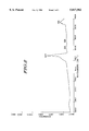
- FIG. 2 is a FTIR (Fourier transform infrared) spectra which is representative of a low temperature annealed spin-on-glass formed in accordance with the present invention.
- Silicate SOGs do not planarize sufficiently and create large stresses in a semiconducting substrate due to a high degree of shrinkage.
- the more widely used siloxane SOGs have improved step coverage and reduced stress, but have a disadvantage of containing organics which can affect performance and reliability of a semiconductor device.
- siloxane SOGs decompose easily and have a tendency to absorb water.
- the present invention overcomes these problems by using a TEOS based SOG containing tetraethylorthosilicate (TEOS), nitric acid, isopropyl alcohol, and water in a specified range of concentrations.
- TEOS tetraethylorthosilicate
- FIG. 1 Illustrated in FIG. 1 is a process flow for making and using a TEOS based SOC in accordance with the present invention. It is important to note that the volume percentages of FIG. 1 are examples of percentages in accordance with the invention. Variations to these percentages can be made and still be within the scope of the invention.
- TEOS tetraethylorthosilicate
- 65-75% by volume alcohol for instance isopropyl alcohol.
- the other solution is a dilute nitric acid solution which is formed by mixing the equivalent of 70% (by weight) concentrated nitric acid with 85-94% by volume alcohol and 6-10% by volume de-ionized water. While each of the above mentioned ranges are suitable, more preferred ranges are as follows: diluting TEOS with 68-70% by volume alcohol; and diluting 70% nitric acid with 7.5-9.0% de-ionized water and 89-91% alcohol. Both of the nitric acid solution and TEOS solution are simply dilutions; therefore, it is not necessary to allow the solutions to react.
- the dilute TEOS solution and the dilute nitric acid solution are then combined in a 1:1 to 1:2 ratio, or more preferably in a ratio of 1:1.2 to 1:1.4, and thoroughly mixed, thereby forming a TEOS based SOG in accordance with the invention.
- SOG it is important that two separate solutions, namely the dilute TEOS solution and the dilute nitric solution, be prepared individually and then combined. Simply mixing all the ingredient will not result in a material suited for use as a spin-on-glass having the properties herein described.
- the resulting SOG has a composition of approximately 15-22% TEOS, 0.2-1.3% concentrated nitric acid, 70-90% alcohol, and the balance being water.
- Other suitable compositions of the inventive SOGs range from 10-25% TEOS, 0.1-3.0% concentrated nitric acid, 60-90% alcohol, and the balance being water.
- Preferred compositions of a TEOS based spin-on-glass in accordance with the present invention fall in the ranges of 16.8-19% TEOS, 0.4-1.1% concentrated nitric acid, 74.5-81.5% alcohol, and the balance being water. All of the mentioned percentages are percentages by volume. The true chemical formula of the SOG cannot readily be determined.
- the resulting SOG is filtered prior to application on a substrate in order to remove particulates which may be present. Particulates can easily be removed through a 0.2 micron filter, resulting in a very clean SOG. Larger or smaller filters can be used, depending on the desired purity of the SOG.
- the filtered SOG is then ready for application onto a substrate, such as a semiconductor wafer. Conventional application techniques are used to apply the SOG to the 10 wafer. A predetermined amount of the SOc is deposited in approximately the center of the wafer. The wafer is then spun to distribute the SOG evenly across the wafer surface.
- the wafer After spinning, the wafer is baked in a traditional manner, for instance using hot plate bakes or oven bakes ranging from 100°-300° C. Baking the wafer drives off water and solvents in the film and converts the SOG to a solid. Additional bakes or anneals may also be required, depending on the application for which the SOG is to be used.
- Each of the TEOS solutions and nitric acid solutions of SOG A and SOG B were made separately, as required by the invention.
- the respective TEOS solutions and nitric acid solutions were then mixed in a ratio of 1:1.2 to 1:1.4 to form SOGs A and B.
- the approximate total volume percentages of SOGs A and B are as follows:
- Each SOG was filtered through a 0.2 micron filter to remove particulates.
- SOGs A and B were then deposited and spun over semiconductor wafers having various topographies. Other process parameters, including spin speed, baking time, baking temperature, and the number of SOG coats applied, were varied to understand the full range of properties of the SOGs.
- SOGs formed and deposited in accordance with the present invention have a minimal reduction in film thickness and minimal stress.
- FIG. 2 Illustrated in FIG. 2 is an FTIR (Fourier transform infrared) spectra of SOG A prior to a high temperature anneal.
- An FTIR spectra provides useful information about the types of chemical bonds present in a material.
- a particular type of chemical bond has a unique corresponding wavenumber.
- the FTIR spectra of FIG. 2 illustrates a peak at an approximate wavenumber of 1077 (cm -1 ). This wavenumber corresponds to an abundance of Si-O bonds. Recall from the background discussion that all SOGs have Si-O bonds.
- FIG. 2 does not illustrate any peaks in the range of wavenumbers from 1470-2950 (cm -1 ).
- SOGs in accordance with the present invention do not have these shortcomings.
- SOG A as described earlier demonstrated minimal shrinkage in film thickness.
- SOG A was deposited onto substrates and spun at 6000 rpm. The films were cured on a hot plate at 300° C. for 1 minute, resulting in a deposited single film thickness of 1,000-1,300 ⁇ . In total, five coats were applied to the substrates to achieve film thicknesses in the range of 5,700-6,100A. The substrates were annealed at various temperatures and the final film thicknesses were measured. The results are shown in the table below:
- the TEOS based SOGs made and used in accordance with the invention are stable and insensitive to the environment. In other words, the SOGs can be exposed to the environment for long periods of time without degradation.
- Existing SOGs typically have a shelf-life of approximately 3-12 months at room temperature while stored in air-tight containers. Exposure to air usually degrades the characteristics of the material.
- SOGs which are part of the present invention have exhibited extended room-temperature shelf-lives in completely open containers without degradation.
- Another uncommon characteristic of a SOG formed in accordance with the present invention is that the SOG is very acidic, well below a pH of 2.
- the pH of the SOG is less than 0; however, the true pH is not readily determinable with conventional water based pH indicators. Having such a low pH is thought to be advantageous because the SOG has properties which are typically characteristic of colloidal solutions without having large particles. However beyond a certain acid concentration, large particles begin to form which make the material inappropriate for use as a spin-on-glass.
- the present invention provides distinct advantages over existing spin-on-glasses and their known applications.
- the present invention permits a SOG to be deposited very thick without cracking and has minimal loss of thickness after cure.
- the present invention provides uniform planarity and can planarize very large spaces.
- Another significant advantage is that a SOG made and used in accordance with the invention has a negligible organic content.
- the SOG can also be used as a passivation layer, particularly if upon exposure to a nitrogen plasma the SOG can be converted to a silicon oxy-nitride.
- Another application is for trench filling. To improve packing density of an integrated circuit, many semiconductor manufacturers use trenches to build elements such as transistors and capacitors. These trenches must eventually be filled to become planar with the rest of the semiconductor wafer before subsequent processing steps are performed. The reported properties of the present invention make the inventive SOG an excellent material for filling trenches in a semiconductor device.
- Yet another application for the present invention is as an alternative to PSG (phosphosilicate glass) or BPSG (boron dopes PSG). By doping the TEOS used in the present invention, the resulting TEOS based SOG will be doped and can function as conventional PSG and BPSG layers in a semiconductor device.
Landscapes
- Formation Of Insulating Films (AREA)
Abstract
Description
______________________________________
                         SOG A   SOG B
                         Volume  Volume
                         %       %
______________________________________
TEOS        TEOS         31.3    31.3
Solution    Isopropyl    68.7    68.7
            Alcohol
Nitric Acid 70% Nitric   2.2     1.1
Solution    Acid
            Isopropyl    89.8    90.3
            Alcohol
            De-Ionized   8.0     8.6
            Water
______________________________________
______________________________________
               SOG A     SOG B
               Tot. Vol. %
                         Tot. Vol. %
______________________________________
TEOS           17.9      18.0
Isopropyl      77.7      77.9
Alcohol
HNO.sub.3 (70%)
               1.0       0.5
Water          3.4       3.6
               100.0     100.0
______________________________________
______________________________________
                       Final      Thickness
Temp. (°C.)
         Anneal Condition
                       Thickness (A)
                                  Lost (%)
______________________________________
300°
         hot plate, 1 minute
                       5,900 ± 200
                                  --
400°
         air, 30-60 minutes
                       5,850 ± 200
                                  0.9
850°
         air, 30 minutes
                       5,600 ± 150
                                  5.1
1100°
         steam, 10 minutes
                       4,850 ± 150
                                  17.8
______________________________________
Claims (3)
Priority Applications (1)
| Application Number | Priority Date | Filing Date | Title |
|---|---|---|---|
| US07/965,314 US5817582A (en) | 1991-02-04 | 1992-10-23 | Process for making a semiconductor device having a TEOS based spin-on-glass |
Applications Claiming Priority (2)
| Application Number | Priority Date | Filing Date | Title |
|---|---|---|---|
| US07/650,119 US5186745A (en) | 1991-02-04 | 1991-02-04 | Teos based spin-on-glass and processes for making and using the same |
| US07/965,314 US5817582A (en) | 1991-02-04 | 1992-10-23 | Process for making a semiconductor device having a TEOS based spin-on-glass |
Related Parent Applications (1)
| Application Number | Title | Priority Date | Filing Date |
|---|---|---|---|
| US07/650,119 Division US5186745A (en) | 1991-02-04 | 1991-02-04 | Teos based spin-on-glass and processes for making and using the same |
Publications (1)
| Publication Number | Publication Date |
|---|---|
| US5817582A true US5817582A (en) | 1998-10-06 |
Family
ID=24607544
Family Applications (2)
| Application Number | Title | Priority Date | Filing Date |
|---|---|---|---|
| US07/650,119 Expired - Fee Related US5186745A (en) | 1991-02-04 | 1991-02-04 | Teos based spin-on-glass and processes for making and using the same |
| US07/965,314 Expired - Fee Related US5817582A (en) | 1991-02-04 | 1992-10-23 | Process for making a semiconductor device having a TEOS based spin-on-glass |
Family Applications Before (1)
| Application Number | Title | Priority Date | Filing Date |
|---|---|---|---|
| US07/650,119 Expired - Fee Related US5186745A (en) | 1991-02-04 | 1991-02-04 | Teos based spin-on-glass and processes for making and using the same |
Country Status (5)
| Country | Link |
|---|---|
| US (2) | US5186745A (en) |
| EP (1) | EP0498604B1 (en) |
| JP (1) | JPH04343227A (en) |
| DE (1) | DE69214683T2 (en) |
| HK (1) | HK1005759A1 (en) |
Cited By (14)
| Publication number | Priority date | Publication date | Assignee | Title |
|---|---|---|---|---|
| US6037275A (en) * | 1998-08-27 | 2000-03-14 | Alliedsignal Inc. | Nanoporous silica via combined stream deposition |
| US6071807A (en) * | 1996-12-25 | 2000-06-06 | Sanyo Electric Company, Ltd. | Fabrication method of semiconductor device including insulation film with decomposed organic content |
| US6177343B1 (en) | 1995-09-14 | 2001-01-23 | Sanyo Electric Co., Ltd. | Process for producing semiconductor devices including an insulating layer with an impurity |
| US6214749B1 (en) * | 1994-09-14 | 2001-04-10 | Sanyo Electric Co., Ltd. | Process for producing semiconductor devices |
| US6235648B1 (en) | 1997-09-26 | 2001-05-22 | Sanyo Electric Co., Ltd. | Semiconductor device including insulation film and fabrication method thereof |
| US6288438B1 (en) | 1996-09-06 | 2001-09-11 | Sanyo Electric Co., Ltd. | Semiconductor device including insulation film and fabrication method thereof |
| US6326318B1 (en) | 1995-09-14 | 2001-12-04 | Sanyo Electric Co., Ltd. | Process for producing semiconductor devices including an insulating layer with an impurity |
| US20030116853A1 (en) * | 2001-12-07 | 2003-06-26 | Naoteru Matsubara | Semiconductor device and method of fabricating the same |
| US6690084B1 (en) | 1997-09-26 | 2004-02-10 | Sanyo Electric Co., Ltd. | Semiconductor device including insulation film and fabrication method thereof |
| US6794283B2 (en) | 1998-05-29 | 2004-09-21 | Sanyo Electric Co., Ltd. | Semiconductor device and fabrication method thereof |
| US6825132B1 (en) | 1996-02-29 | 2004-11-30 | Sanyo Electric Co., Ltd. | Manufacturing method of semiconductor device including an insulation film on a conductive layer |
| US6831015B1 (en) | 1996-08-30 | 2004-12-14 | Sanyo Electric Co., Ltd. | Fabrication method of semiconductor device and abrasive liquid used therein |
| US20060199371A1 (en) * | 1995-09-14 | 2006-09-07 | Sanyo Electric Co., Ltd. | Semiconductor devices passivation film |
| US20070173074A1 (en) * | 2000-02-02 | 2007-07-26 | Min-Jin Ko | Semiconductor interlayer dielectric material and a semiconductor device using the same |
Families Citing this family (17)
| Publication number | Priority date | Publication date | Assignee | Title |
|---|---|---|---|---|
| JPH04233732A (en) * | 1990-08-16 | 1992-08-21 | Motorola Inc | Spin on derivative used in manufacturing process of semiconductor |
| US5472488A (en) * | 1990-09-14 | 1995-12-05 | Hyundai Electronics America | Coating solution for forming glassy layers |
| US5527872A (en) * | 1990-09-14 | 1996-06-18 | At&T Global Information Solutions Company | Electronic device with a spin-on glass dielectric layer |
| US5322805A (en) * | 1992-10-16 | 1994-06-21 | Ncr Corporation | Method for forming a bipolar emitter using doped SOG |
| US5393702A (en) * | 1993-07-06 | 1995-02-28 | United Microelectronics Corporation | Via sidewall SOG nitridation for via filling |
| US5801076A (en) * | 1995-02-21 | 1998-09-01 | Advanced Micro Devices, Inc. | Method of making non-volatile memory device having a floating gate with enhanced charge retention |
| US5510147A (en) * | 1995-03-03 | 1996-04-23 | International Paper Company | Sol gel barrier films |
| US5847444A (en) * | 1995-09-14 | 1998-12-08 | Nec Corporation | Semiconductor device with reduced aspect ratio contact hole |
| US7067442B1 (en) * | 1995-12-26 | 2006-06-27 | Micron Technology, Inc. | Method to avoid threshold voltage shift in thicker dielectric films |
| US6166439A (en) * | 1997-12-30 | 2000-12-26 | Advanced Micro Devices, Inc. | Low dielectric constant material and method of application to isolate conductive lines |
| WO2006022259A1 (en) * | 2004-08-24 | 2006-03-02 | Sharp Kabushiki Kaisha | Active matrix substrate and display unit provided with it |
| US7943410B2 (en) | 2008-12-10 | 2011-05-17 | Stmicroelectronics, Inc. | Embedded microelectromechanical systems (MEMS) semiconductor substrate and related method of forming |
| US9249028B2 (en) | 2010-02-08 | 2016-02-02 | Momentive Performance Materials Inc. | Method for making high purity metal oxide particles and materials made thereof |
| US8197782B2 (en) * | 2010-02-08 | 2012-06-12 | Momentive Performance Materials | Method for making high purity metal oxide particles and materials made thereof |
| US9514932B2 (en) | 2012-08-08 | 2016-12-06 | Applied Materials, Inc. | Flowable carbon for semiconductor processing |
| US9362107B2 (en) | 2014-09-30 | 2016-06-07 | Applied Materials, Inc. | Flowable low-k dielectric gapfill treatment |
| CN117447234A (en) * | 2023-10-17 | 2024-01-26 | 夸泰克(广州)新材料有限责任公司 | A method for preparing ultra-high temperature resistant spin-coated glass film layer |
Citations (6)
| Publication number | Priority date | Publication date | Assignee | Title |
|---|---|---|---|---|
| US4619839A (en) * | 1984-12-12 | 1986-10-28 | Fairchild Camera & Instrument Corp. | Method of forming a dielectric layer on a semiconductor device |
| US4654269A (en) * | 1985-06-21 | 1987-03-31 | Fairchild Camera & Instrument Corp. | Stress relieved intermediate insulating layer for multilayer metalization |
| US4771016A (en) * | 1987-04-24 | 1988-09-13 | Harris Corporation | Using a rapid thermal process for manufacturing a wafer bonded soi semiconductor |
| US4798629A (en) * | 1987-10-22 | 1989-01-17 | Motorola Inc. | Spin-on glass for use in semiconductor processing |
| US4826709A (en) * | 1988-02-29 | 1989-05-02 | American Telephone And Telegraph Company At&T Bell Laboratories | Devices involving silicon glasses |
| US4842901A (en) * | 1987-02-13 | 1989-06-27 | Hoechst Aktiengesellschaft | Coating solution and process for producing glassy layers |
Family Cites Families (5)
| Publication number | Priority date | Publication date | Assignee | Title |
|---|---|---|---|---|
| JPS6031227B2 (en) * | 1977-05-30 | 1985-07-20 | 関西ペイント株式会社 | Method for producing vehicle for heat-resistant paint |
| DE2944180A1 (en) * | 1979-11-02 | 1981-05-07 | Licentia Patent-Verwaltungs-Gmbh, 6000 Frankfurt | METHOD FOR PRODUCING AN INSULATION LAYER COVERING A SEMICONDUCTOR BODY ON ONE SIDE |
| US4535026A (en) * | 1983-06-29 | 1985-08-13 | The United States Of America As Represented By The United States Department Of Energy | Antireflective graded index silica coating, method for making |
| EP0206717A3 (en) * | 1985-06-17 | 1988-08-24 | Nissan Chemical Industries Ltd. | Coating compositions |
| JPH01111709A (en) * | 1987-10-23 | 1989-04-28 | Hitachi Chem Co Ltd | Production of hydroxysilane and/or its oligomer |
-
1991
- 1991-02-04 US US07/650,119 patent/US5186745A/en not_active Expired - Fee Related
-
1992
- 1992-02-03 DE DE69214683T patent/DE69214683T2/en not_active Expired - Fee Related
- 1992-02-03 EP EP92300908A patent/EP0498604B1/en not_active Expired - Lifetime
- 1992-02-04 JP JP4047583A patent/JPH04343227A/en active Pending
- 1992-10-23 US US07/965,314 patent/US5817582A/en not_active Expired - Fee Related
-
1998
- 1998-06-04 HK HK98104879A patent/HK1005759A1/en not_active IP Right Cessation
Patent Citations (6)
| Publication number | Priority date | Publication date | Assignee | Title |
|---|---|---|---|---|
| US4619839A (en) * | 1984-12-12 | 1986-10-28 | Fairchild Camera & Instrument Corp. | Method of forming a dielectric layer on a semiconductor device |
| US4654269A (en) * | 1985-06-21 | 1987-03-31 | Fairchild Camera & Instrument Corp. | Stress relieved intermediate insulating layer for multilayer metalization |
| US4842901A (en) * | 1987-02-13 | 1989-06-27 | Hoechst Aktiengesellschaft | Coating solution and process for producing glassy layers |
| US4771016A (en) * | 1987-04-24 | 1988-09-13 | Harris Corporation | Using a rapid thermal process for manufacturing a wafer bonded soi semiconductor |
| US4798629A (en) * | 1987-10-22 | 1989-01-17 | Motorola Inc. | Spin-on glass for use in semiconductor processing |
| US4826709A (en) * | 1988-02-29 | 1989-05-02 | American Telephone And Telegraph Company At&T Bell Laboratories | Devices involving silicon glasses |
Cited By (17)
| Publication number | Priority date | Publication date | Assignee | Title |
|---|---|---|---|---|
| US6214749B1 (en) * | 1994-09-14 | 2001-04-10 | Sanyo Electric Co., Ltd. | Process for producing semiconductor devices |
| US6177343B1 (en) | 1995-09-14 | 2001-01-23 | Sanyo Electric Co., Ltd. | Process for producing semiconductor devices including an insulating layer with an impurity |
| US20060199371A1 (en) * | 1995-09-14 | 2006-09-07 | Sanyo Electric Co., Ltd. | Semiconductor devices passivation film |
| US6268657B1 (en) | 1995-09-14 | 2001-07-31 | Sanyo Electric Co., Ltd. | Semiconductor devices and an insulating layer with an impurity |
| US6326318B1 (en) | 1995-09-14 | 2001-12-04 | Sanyo Electric Co., Ltd. | Process for producing semiconductor devices including an insulating layer with an impurity |
| US6825132B1 (en) | 1996-02-29 | 2004-11-30 | Sanyo Electric Co., Ltd. | Manufacturing method of semiconductor device including an insulation film on a conductive layer |
| US6831015B1 (en) | 1996-08-30 | 2004-12-14 | Sanyo Electric Co., Ltd. | Fabrication method of semiconductor device and abrasive liquid used therein |
| US6288438B1 (en) | 1996-09-06 | 2001-09-11 | Sanyo Electric Co., Ltd. | Semiconductor device including insulation film and fabrication method thereof |
| US6071807A (en) * | 1996-12-25 | 2000-06-06 | Sanyo Electric Company, Ltd. | Fabrication method of semiconductor device including insulation film with decomposed organic content |
| US6235648B1 (en) | 1997-09-26 | 2001-05-22 | Sanyo Electric Co., Ltd. | Semiconductor device including insulation film and fabrication method thereof |
| US6690084B1 (en) | 1997-09-26 | 2004-02-10 | Sanyo Electric Co., Ltd. | Semiconductor device including insulation film and fabrication method thereof |
| US6794283B2 (en) | 1998-05-29 | 2004-09-21 | Sanyo Electric Co., Ltd. | Semiconductor device and fabrication method thereof |
| US6037275A (en) * | 1998-08-27 | 2000-03-14 | Alliedsignal Inc. | Nanoporous silica via combined stream deposition |
| US20070173074A1 (en) * | 2000-02-02 | 2007-07-26 | Min-Jin Ko | Semiconductor interlayer dielectric material and a semiconductor device using the same |
| US7470636B2 (en) * | 2000-02-02 | 2008-12-30 | Lg Chem, Ltd. | Semiconductor interlayer dielectric material and a semiconductor device using the same |
| US20030116853A1 (en) * | 2001-12-07 | 2003-06-26 | Naoteru Matsubara | Semiconductor device and method of fabricating the same |
| US6917110B2 (en) | 2001-12-07 | 2005-07-12 | Sanyo Electric Co., Ltd. | Semiconductor device comprising an interconnect structure with a modified low dielectric insulation layer |
Also Published As
| Publication number | Publication date |
|---|---|
| DE69214683T2 (en) | 1997-04-30 |
| EP0498604A1 (en) | 1992-08-12 |
| DE69214683D1 (en) | 1996-11-28 |
| JPH04343227A (en) | 1992-11-30 |
| US5186745A (en) | 1993-02-16 |
| HK1005759A1 (en) | 1999-01-22 |
| EP0498604B1 (en) | 1996-10-23 |
Similar Documents
| Publication | Publication Date | Title |
|---|---|---|
| US5186745A (en) | Teos based spin-on-glass and processes for making and using the same | |
| HK1005759B (en) | Semiconductor device having a teos based spin-on-glass and process for making the same | |
| USRE39690E1 (en) | Enhanced planarization technique for an integrated circuit | |
| US6204202B1 (en) | Low dielectric constant porous films | |
| JP3568537B2 (en) | Electron beam processed film for microelectronic structure | |
| US4676867A (en) | Planarization process for double metal MOS using spin-on glass as a sacrificial layer | |
| EP1169491B1 (en) | Low dielectric nano-porous material obtainable from polymer decomposition | |
| US6413882B1 (en) | Low dielectric foam dielectric formed from polymer decomposition | |
| US20020137260A1 (en) | Dielectric films for narrow gap-fill applications | |
| US20030087485A1 (en) | Dielectric films for narrow gap-fill applications | |
| JP2003517713A (en) | Porous insulating compound and method for producing the same | |
| US20040228967A1 (en) | Dielectric films for narrow gap-fill applications | |
| US20020019145A1 (en) | Deposition of nanoporous silica films using a closed cup coater | |
| KR20050013492A (en) | Improved chemical planarization performance for copper/low-k interconnect structures | |
| WO1998047943A1 (en) | Stable inorganic polymers | |
| US6809041B2 (en) | Low dielectric constant films derived by sol-gel processing of a hyperbranched polycarbosilane | |
| EP1118110A1 (en) | Process for optimizing mechanical strength of nanoporous silica | |
| US6727184B1 (en) | Method for coating a thick spin-on-glass layer on a semiconductor structure | |
| US4619839A (en) | Method of forming a dielectric layer on a semiconductor device | |
| KR100455886B1 (en) | Semiconductor device fabrication method | |
| JPH118239A (en) | Method for manufacturing semiconductor device | |
| EP0424638A2 (en) | Fabrication of a semiconductor device including a step for prodiving a layer of insulating material formed from an organo-silica sol | |
| US5910680A (en) | Germanium silicate spin on glass semiconductor device and methods of spin on glass synthesis and use | |
| US6827982B1 (en) | Binder-enriched silicalite adhesion layer and apparatus for fabricating the same | |
| Madayag et al. | Optimization of spin-on-glass process for multilevel metal interconnects |
Legal Events
| Date | Code | Title | Description |
|---|---|---|---|
| FPAY | Fee payment |
Year of fee payment: 4 |
|
| AS | Assignment |
Owner name: FREESCALE SEMICONDUCTOR, INC., TEXAS Free format text: ASSIGNMENT OF ASSIGNORS INTEREST;ASSIGNOR:MOTOROLA, INC.;REEL/FRAME:015698/0657 Effective date: 20040404 Owner name: FREESCALE SEMICONDUCTOR, INC.,TEXAS Free format text: ASSIGNMENT OF ASSIGNORS INTEREST;ASSIGNOR:MOTOROLA, INC.;REEL/FRAME:015698/0657 Effective date: 20040404 |
|
| REMI | Maintenance fee reminder mailed | ||
| LAPS | Lapse for failure to pay maintenance fees | ||
| STCH | Information on status: patent discontinuation |
Free format text: PATENT EXPIRED DUE TO NONPAYMENT OF MAINTENANCE FEES UNDER 37 CFR 1.362 |
|
| FP | Lapsed due to failure to pay maintenance fee |
Effective date: 20061006 |