US5804455A - Reduced primary crystalline defect damage in NMOSFETS with an optimized LDD structure - Google Patents
Reduced primary crystalline defect damage in NMOSFETS with an optimized LDD structure Download PDFInfo
- Publication number
- US5804455A US5804455A US08/625,874 US62587496A US5804455A US 5804455 A US5804455 A US 5804455A US 62587496 A US62587496 A US 62587496A US 5804455 A US5804455 A US 5804455A
- Authority
- US
- United States
- Prior art keywords
- layer
- substrate
- polysilicon
- gate region
- silicon oxide
- Prior art date
- Legal status (The legal status is an assumption and is not a legal conclusion. Google has not performed a legal analysis and makes no representation as to the accuracy of the status listed.)
- Expired - Lifetime
Links
- 230000007547 defect Effects 0.000 title claims abstract description 15
- 229910021420 polycrystalline silicon Inorganic materials 0.000 claims abstract description 42
- 229920005591 polysilicon Polymers 0.000 claims abstract description 42
- 239000000758 substrate Substances 0.000 claims abstract description 35
- XUIMIQQOPSSXEZ-UHFFFAOYSA-N Silicon Chemical compound [Si] XUIMIQQOPSSXEZ-UHFFFAOYSA-N 0.000 claims abstract description 22
- 229910052710 silicon Inorganic materials 0.000 claims abstract description 21
- 238000000034 method Methods 0.000 claims abstract description 20
- 238000005468 ion implantation Methods 0.000 claims abstract description 19
- 239000010703 silicon Substances 0.000 claims abstract description 19
- 125000006850 spacer group Chemical group 0.000 claims abstract description 7
- 238000002513 implantation Methods 0.000 claims 1
- VYPSYNLAJGMNEJ-UHFFFAOYSA-N Silicium dioxide Chemical compound O=[Si]=O VYPSYNLAJGMNEJ-UHFFFAOYSA-N 0.000 abstract description 28
- 229910052814 silicon oxide Inorganic materials 0.000 abstract description 28
- 238000005530 etching Methods 0.000 abstract description 19
- 229920002120 photoresistant polymer Polymers 0.000 abstract description 18
- 239000004065 semiconductor Substances 0.000 abstract description 5
- CPELXLSAUQHCOX-UHFFFAOYSA-N Hydrogen bromide Chemical compound Br CPELXLSAUQHCOX-UHFFFAOYSA-N 0.000 description 8
- 150000002500 ions Chemical class 0.000 description 7
- 238000005229 chemical vapour deposition Methods 0.000 description 6
- 239000007789 gas Substances 0.000 description 5
- 230000008901 benefit Effects 0.000 description 4
- 230000015572 biosynthetic process Effects 0.000 description 4
- 229910000042 hydrogen bromide Inorganic materials 0.000 description 4
- 239000007943 implant Substances 0.000 description 4
- 238000004519 manufacturing process Methods 0.000 description 3
- 238000000137 annealing Methods 0.000 description 2
- 239000002019 doping agent Substances 0.000 description 2
- 239000012535 impurity Substances 0.000 description 2
- 239000000463 material Substances 0.000 description 2
- -1 phosphorous ions Chemical class 0.000 description 2
- XHXFXVLFKHQFAL-UHFFFAOYSA-N phosphoryl trichloride Chemical compound ClP(Cl)(Cl)=O XHXFXVLFKHQFAL-UHFFFAOYSA-N 0.000 description 2
- XPDWGBQVDMORPB-UHFFFAOYSA-N Fluoroform Chemical compound FC(F)F XPDWGBQVDMORPB-UHFFFAOYSA-N 0.000 description 1
- BLRPTPMANUNPDV-UHFFFAOYSA-N Silane Chemical compound [SiH4] BLRPTPMANUNPDV-UHFFFAOYSA-N 0.000 description 1
- BOTDANWDWHJENH-UHFFFAOYSA-N Tetraethyl orthosilicate Chemical compound CCO[Si](OCC)(OCC)OCC BOTDANWDWHJENH-UHFFFAOYSA-N 0.000 description 1
- XMIJDTGORVPYLW-UHFFFAOYSA-N [SiH2] Chemical compound [SiH2] XMIJDTGORVPYLW-UHFFFAOYSA-N 0.000 description 1
- 229910052785 arsenic Inorganic materials 0.000 description 1
- 238000010420 art technique Methods 0.000 description 1
- 229910021419 crystalline silicon Inorganic materials 0.000 description 1
- 230000005284 excitation Effects 0.000 description 1
- 230000003647 oxidation Effects 0.000 description 1
- 238000007254 oxidation reaction Methods 0.000 description 1
- 230000000717 retained effect Effects 0.000 description 1
Images


Classifications
-
- H—ELECTRICITY
- H01—ELECTRIC ELEMENTS
- H01L—SEMICONDUCTOR DEVICES NOT COVERED BY CLASS H10
- H01L21/00—Processes or apparatus adapted for the manufacture or treatment of semiconductor or solid state devices or of parts thereof
- H01L21/02—Manufacture or treatment of semiconductor devices or of parts thereof
- H01L21/04—Manufacture or treatment of semiconductor devices or of parts thereof the devices having at least one potential-jump barrier or surface barrier, e.g. PN junction, depletion layer or carrier concentration layer
- H01L21/18—Manufacture or treatment of semiconductor devices or of parts thereof the devices having at least one potential-jump barrier or surface barrier, e.g. PN junction, depletion layer or carrier concentration layer the devices having semiconductor bodies comprising elements of Group IV of the Periodic System or AIIIBV compounds with or without impurities, e.g. doping materials
- H01L21/26—Bombardment with radiation
- H01L21/263—Bombardment with radiation with high-energy radiation
- H01L21/265—Bombardment with radiation with high-energy radiation producing ion implantation
- H01L21/26506—Bombardment with radiation with high-energy radiation producing ion implantation in group IV semiconductors
- H01L21/26513—Bombardment with radiation with high-energy radiation producing ion implantation in group IV semiconductors of electrically active species
- H01L21/2652—Through-implantation
-
- H—ELECTRICITY
- H01—ELECTRIC ELEMENTS
- H01L—SEMICONDUCTOR DEVICES NOT COVERED BY CLASS H10
- H01L29/00—Semiconductor devices adapted for rectifying, amplifying, oscillating or switching, or capacitors or resistors with at least one potential-jump barrier or surface barrier, e.g. PN junction depletion layer or carrier concentration layer; Details of semiconductor bodies or of electrodes thereof ; Multistep manufacturing processes therefor
- H01L29/66—Types of semiconductor device ; Multistep manufacturing processes therefor
- H01L29/66007—Multistep manufacturing processes
- H01L29/66075—Multistep manufacturing processes of devices having semiconductor bodies comprising group 14 or group 13/15 materials
- H01L29/66227—Multistep manufacturing processes of devices having semiconductor bodies comprising group 14 or group 13/15 materials the devices being controllable only by the electric current supplied or the electric potential applied, to an electrode which does not carry the current to be rectified, amplified or switched, e.g. three-terminal devices
- H01L29/66409—Unipolar field-effect transistors
- H01L29/66477—Unipolar field-effect transistors with an insulated gate, i.e. MISFET
- H01L29/66568—Lateral single gate silicon transistors
- H01L29/66575—Lateral single gate silicon transistors where the source and drain or source and drain extensions are self-aligned to the sides of the gate
- H01L29/6659—Lateral single gate silicon transistors where the source and drain or source and drain extensions are self-aligned to the sides of the gate with both lightly doped source and drain extensions and source and drain self-aligned to the sides of the gate, e.g. lightly doped drain [LDD] MOSFET, double diffused drain [DDD] MOSFET
Definitions
- the present invention relates to semiconductor IC manufacture.
- the present invention relates to a method for forming a MOSFET with an LDD (Lightly Doped Drain) structure with reduced primary crystalline defect damage.
- LDD Lightly Doped Drain
- Ion implantation is a technique that has been widely used in VLSI processing. Ion implantation has many advantages for VLSI processing, the most important being the ability to control the number of impurity atoms introduced into a silicon substrate more precisely. The price for such benefits is high, because ion implantation cannot be performed without damage to the silicon substrate.
- energetic ions enter a silicon substrate, they lose their energy in a series of nuclear and electron collisions and finally come to rest. The electron-energy loss can be accounted for in terms of electronic excitations to higher energy levels or in the generation of electron-hole pairs.
- electron collisions do not displace silicon atoms from their lattice positions. Only nuclear collisions can transfer sufficient energy to the lattice so that host atoms are displaced resulting in lattice disorder. The lattice in these disordered regions exhibits several different damage configurations:
- Type (c) will be referred to as amorphous layer damage since the damage annealing procedure for type (a) and (b) are the same, but a different damage annealing procedure is employed for type (c).
- FIGS. 1A through 1G A typical process for the formation of NMOSFET's with a conventional LDD structure is shown in FIGS. 1A through 1G.
- a semiconductor structure 10 is provided having a thin silicon oxide layer 14 (gate dielectric) on a silicon substrate 12.
- a polysilicon layer 16 is formed on the thin silicon oxide layer 14.
- the substrate 12 is P-type.
- a first photoresist mask layer 18 is formed on the polysilicon layer 16 and patterned. Only a gate region 20 of the polysilicon layer 16 is covered by the remaining first photoresist mask layer 18.
- an anisotropic etching is performed.
- the exposed polysilicon is anisotropically etched so that only the gate region 20 remains.
- the first photoresist mask layer 18 is removed.
- a first ion implantation 21 is performed and wide N-regions 22 and 24 with primary crystalline defect damage are formed on either side of the gate region 20.
- a layer of undoped silicon oxide 26 is deposited on all exposed surface areas.
- an anisotropic etching is used first on the undoped silicon oxide 26 and then the gate oxide 14 until the silicon substrate that is not under cover of polysilicon gate region 20 is exposed, such that residues of undoped silicon oxide remain on the vertical edges of the polysilicon gate region 20 to act as spacers 30.
- a second ion implantation 32 is performed to form heavily doped regions 34, 36 that act as source/drain regions.
- NMOSFET 10 shown in FIG. 1G comprising a P-substrate 12, a gate structure comprising gate oxide 14, polysilicon gate 20, and spacers 30, and LDD type source/drain regions.
- Each source/drain region comprises a lightly doped N-type region 22 or 24 and a heavily doped N-type region 34 or 36.
- a problem with the prior art process used to form the LDD structure is that the lightly doped regions 22, 24 occupy a relatively large region of the substrate. As these regions are formed by low dose implants of heavy ions, there is significant primary crystalline defect damage in these regions of the substrate.
- a method for forming a MOSFET device, such as an NMOSFET, with a Lightly Doped Drain (LDD) structure with reduced primary crystalline defect damage is disclosed.
- a semiconductor structure is provided having a thin silicon oxide layer (gate dielectric) on a silicon substrate.
- a polysilicon layer is formed on the thin silicon oxide layer.
- a photoresist mask is formed on the polysilicon layer. The photoresist mask is patterned to form two narrow slit openings through which the polysilicon layer is exposed. The exposed polysilicon is anisotropically etched. This defines a gate region between the two narrow slit openings.
- a first ion implantation now takes place to form two lightly doped regions in the substrate on either side of the gate region.
- the ion implantation takes place only through the slits so that the implanted regions in the substrate are also narrow. This significantly limits the region of the substrate in which there is primary crystalline defect damage and is a significant advantage of the invention.
- the first photoresist mask layer is removed.
- a second photoresist mask is formed on all exposed surface areas and patterned so that only the gate region of the polysilicon layer is covered by the second photoresist mask.
- the exposed portions of the polysilicon layer are anisotropically etched and the remaining second photoresist mask layer is removed.
- a layer of undoped silicon oxide is deposited on all exposed surface areas.
- Anisotropic etching is used first on the undoped silicon oxide until the silicon substrate that is not under the polysilicon layer is exposed, such that residues of undoped silicon oxide remain on the vertical edges of the polysilicon gate region to act as spacers.
- a second ion implantation is then performed on both sides of the gate region to form heavily doped regions that act as source/drain regions.
- FIGS. 1A through 1G illustrate a prior art method of manufacturing an NMOSFET.
- FIGS. 2 through 11 illustrate the inventive method of manufacturing an NMOSFET so that the primary crystalline defect damage will be effectively reduced.
- a P-type silicon substrate 12 is covered by a thin silicon oxide layer 14 (gate oxide).
- the thin silicon oxide layer ranges in thickness from 70 to 300 Angstroms, and functions as the gate dielectric.
- Other materials may also be used for the gate dielectric.
- the gate dielectric may be formed by thermal oxidation or chemical vapor deposition (CVD).
- a layer of polysilicon 16 is deposited on the thin silicon oxide layer 14 by chemical vapor deposition (CVD).
- the polysilicon layer 16 ranges in thickness from 1500 to 5000 angstroms.
- the polysilicon layer is then doped with phosphorous oxychloride (POCl 3 ) in a temperature range of about 800° to 1000° C. to reduce the resistance of the polysilicon.
- the polysilicon layer is doped to an impurity concentration of about 1E19 to 1E21/cm**3.
- a first photoresist mask layer 50 is formed on the polysilicon layer 16.
- the photoresist mask layer has narrow slit openings 52,54.
- the uncovered regions of the polysilicon layer 16 are etched away.
- Anisotropic etching is utilized with an etching gas of high selectivity such as hydrogen bromide (HBr/Cl 2 /O 2 ). That is, the etching rate is very high for silicon but very low for silicon oxide.
- the thin silicon oxide layer 14 acts as an etching stop that protects the silicon substrate from damage during the polysilicon etching process.
- a gate region 20 is defined in the polysilicon layer 16 between the slit openings 52, 54.
- the gate electrode region 20 has a width of approximately 0.25 to 0.80 microns and the slit openings 52, 54 have a width of approximately 0.1 to 0.4 microns.
- a first ion implantation 60 is performed to implant N-regions 62, 64 in the silicon substrate below the exposed portions of the thin silicon oxide layer 14.
- phosphorous ions may be used with an energy of about 5 to 70 kev and a dosage of about 1E13 to 6E13/cm**2.
- the N-regions 62, 64 illustratively have a depth of approximately 0.05 to 0.5 microns and a doping concentration of about 1E17 to 1E19/cm**3.
- the first ion implantation takes place through the narrow slit openings.
- the lightly doped regions 62, 64 have approximately the same widths as the slits, i.e., 0.1 to 0.4 microns.
- the region of the substrate which has primary crystalline defect damage is much smaller than when the above-described conventional NMOSFET formation process is used.
- a second photoresist mask layer 70 is formed and patterned, only the gate region 20 is covered by the remaining photoresist mask layer 70.
- the exposed portions of the polysilicon layer 16 are etched away.
- Anisotropic etching is introduced with an etching gas of high selectivity such as hydrogen bromide (HBr/Cl 2 /O 2 ). That is, the etching rate is very high for silicon but very low for silicon oxide.
- the thin silicon oxide layer 14 acts as an etching stop that protects the silicon substrate from damage during the polysilicon etching process.
- a layer of undoped silicon oxide 26 is deposited on all exposed surface areas to a thickness in the range of about 800 to 3000 angstroms by chemical vapor deposition (CVD).
- the reacting gas may be SiH 2 Cl 2 /N 2 O, SiH 4 /O 2 or TEOS/O 2 , at a temperature in the range of about 400° C. to 800° C.
- the undoped silicon oxide layer 26 and the regions of the thin gate oxide 14 that are not covered by the polysilicon gate 20 are etched with a highly selective etching gas until the silicon substrate is exposed.
- the etching rate is very high for silicon oxide but very low for silicon.
- the etching gas may be CHF 3 /CF 4 . Because the etching depth can be controlled by this process, residual amounts of undoped silicon oxide are retained on the vertical edges of the polysilicon gate electrode region 20. These residual undoped silicon oxide regions act as spacers 30.
- a second ion implantation 21 is performed to implant source/drain regions 34, 36 in the silicon substrate 12 beneath the exposed substrate areas.
- arsenic ions may be used with an energy of about 5 to 100 kev and a dosage of about 1E15 to 8E15/cm**2.
- the source/drain regions 34, 36 illustratively have a depth of approximately 0.05 to 0.5 microns, a width of approximately 0.5 to 1.5 microns, and a doping concentration of about 1E20 to 1E21/cm**3.
- the advantage of the invention is significant.
- the size of the lightly doped regions that are formed by the first ion implantation are reduced and the primary crystalline defect damage will be effectively reduced.
- the dopant concentration of source/drain regions that are formed by this new technique are almost the same with the dopant concentration of source/drain regions that are formed by the prior art technique since the dosage of the second ion implantation is about two orders of magnitude greater than the dosage of the first ion implantation.
- the final device structure shown in FIG. 11 is substantially the same as the device structure shown in FIG. 1G.
- the heavily doped regions 34, 36 may overlap at least in part the lightly doped regions 62, 64.
- the heavily doped regions 62, 64 are continuous with the lightly doped regions 34, 36.
- the portions of the lightly doped regions 62, 64 under the spacers are generally not overlapped by the heavily doped regions 34, 36.
Abstract
A method for forming a MOSFET device, having Lightly Doped Drain structures with reduced primary crystalline defect damage wherein a semiconductor structure is provided having a thin silicon oxide layer on a silicon substrate, a polysilicon layer formed on the silicon oxide layer, and a photoresist mask formed on the polysilicon layer. The mask is patterned to form two narrow slit openings through which the polysilicon layer is exposed. The exposed polysilicon is anisotropically etched to define a gate region between the two slits. A first ion implantation forms two lightly doped regions in the substrate on either side of the gate region. The ion implantation takes place through the slits so that the implanted regions in the substrate are narrow. This limits the region of the substrate in which there is primary crystalline defect damage. The first photoresist mask layer is removed. A second photoresist mask layer is formed on all exposed surface areas and patterned so that only the polysilicon gate region is covered. The exposed polysilicon is anisotropically etched and the remaining mask layer is removed. A layer of silicon oxide is deposited on all exposed surface areas. Anisotropic etching is used on the silicon oxide until the substrate not under the polysilicon layer is exposed. Thus, residues of silicon oxide remain on the vertical edges of the gate region to act as spacers. A second ion implantation is performed on both sides of the gate region to form heavily doped regions.
Description
The present invention relates to semiconductor IC manufacture. In particular, the present invention relates to a method for forming a MOSFET with an LDD (Lightly Doped Drain) structure with reduced primary crystalline defect damage.
Ion implantation is a technique that has been widely used in VLSI processing. Ion implantation has many advantages for VLSI processing, the most important being the ability to control the number of impurity atoms introduced into a silicon substrate more precisely. The price for such benefits is high, because ion implantation cannot be performed without damage to the silicon substrate. When energetic ions enter a silicon substrate, they lose their energy in a series of nuclear and electron collisions and finally come to rest. The electron-energy loss can be accounted for in terms of electronic excitations to higher energy levels or in the generation of electron-hole pairs. However, electron collisions do not displace silicon atoms from their lattice positions. Only nuclear collisions can transfer sufficient energy to the lattice so that host atoms are displaced resulting in lattice disorder. The lattice in these disordered regions exhibits several different damage configurations:
(a) isolated point defects or point defect clusters in essentially crystalline silicon (the type of damage that results from implanting light ions, or when En˜2Edi; where En is the energy transferred to a silicon atom and Edi is the energy required to displace silicon atom from its lattice site)
(b) local zones of completely amorphous material in an otherwise crystalline layer (An amorphous region is defined as a region in which the displaced atoms per unit volume approach the atomic density of the semiconductor). This form of damage configuration is associated with low dose implants of heavy ions (En>>Edi); and
(c) continuous amorphous layers which form as the damage from the ions accumulates. That is, as the dose of ions (typically heavy ions) increase, the locally amorphous regions eventually overlap, and a continuous amorphous layer is formed.
It is an established fact that types (a) and (b) are grouped into the category of primary crystalline defect damage. Type (c) will be referred to as amorphous layer damage since the damage annealing procedure for type (a) and (b) are the same, but a different damage annealing procedure is employed for type (c).
A typical process for the formation of NMOSFET's with a conventional LDD structure is shown in FIGS. 1A through 1G.
Shown in FIG. 1A, a semiconductor structure 10 is provided having a thin silicon oxide layer 14 (gate dielectric) on a silicon substrate 12. A polysilicon layer 16 is formed on the thin silicon oxide layer 14. Illustratively, the substrate 12 is P-type.
Shown in FIG. 1B, a first photoresist mask layer 18 is formed on the polysilicon layer 16 and patterned. Only a gate region 20 of the polysilicon layer 16 is covered by the remaining first photoresist mask layer 18.
Shown in FIG. 1C, an anisotropic etching is performed. The exposed polysilicon is anisotropically etched so that only the gate region 20 remains.
Shown in FIG. 1D, the first photoresist mask layer 18 is removed. A first ion implantation 21 is performed and wide N- regions 22 and 24 with primary crystalline defect damage are formed on either side of the gate region 20.
Shown in FIG. 1E, a layer of undoped silicon oxide 26 is deposited on all exposed surface areas.
Shown in FIG. 1F, an anisotropic etching is used first on the undoped silicon oxide 26 and then the gate oxide 14 until the silicon substrate that is not under cover of polysilicon gate region 20 is exposed, such that residues of undoped silicon oxide remain on the vertical edges of the polysilicon gate region 20 to act as spacers 30.
Shown in FIG. 1G, a second ion implantation 32 is performed to form heavily doped regions 34, 36 that act as source/drain regions.
The result of this process is an NMOSFET 10 shown in FIG. 1G comprising a P-substrate 12, a gate structure comprising gate oxide 14, polysilicon gate 20, and spacers 30, and LDD type source/drain regions. Each source/drain region comprises a lightly doped N- type region 22 or 24 and a heavily doped N- type region 34 or 36.
The following prior art references relate to the formation of the LDD structure.
Stanly Wolf "Silicon Process for The VLSI ERA", Lattice Press, Sunset Beach, Calif., 1986
U.S. Patent Documents
U.S. Pat. No. 5,436,176
U.S. Pat. No. 5,384,268
U.S. Pat. No. 5,145,797
A problem with the prior art process used to form the LDD structure is that the lightly doped regions 22, 24 occupy a relatively large region of the substrate. As these regions are formed by low dose implants of heavy ions, there is significant primary crystalline defect damage in these regions of the substrate.
Accordingly, it is an object of the invention to provide an alternate process for making a MOSFET device such as an NMOSFET with LDD source/drain regions in which the primary crystalline damage is confined to a smaller region of the substrate.
A method for forming a MOSFET device, such as an NMOSFET, with a Lightly Doped Drain (LDD) structure with reduced primary crystalline defect damage is disclosed. A semiconductor structure is provided having a thin silicon oxide layer (gate dielectric) on a silicon substrate. A polysilicon layer is formed on the thin silicon oxide layer. A photoresist mask is formed on the polysilicon layer. The photoresist mask is patterned to form two narrow slit openings through which the polysilicon layer is exposed. The exposed polysilicon is anisotropically etched. This defines a gate region between the two narrow slit openings. A first ion implantation now takes place to form two lightly doped regions in the substrate on either side of the gate region. The ion implantation takes place only through the slits so that the implanted regions in the substrate are also narrow. This significantly limits the region of the substrate in which there is primary crystalline defect damage and is a significant advantage of the invention. Then, the first photoresist mask layer is removed. A second photoresist mask is formed on all exposed surface areas and patterned so that only the gate region of the polysilicon layer is covered by the second photoresist mask. The exposed portions of the polysilicon layer are anisotropically etched and the remaining second photoresist mask layer is removed. A layer of undoped silicon oxide is deposited on all exposed surface areas. Anisotropic etching is used first on the undoped silicon oxide until the silicon substrate that is not under the polysilicon layer is exposed, such that residues of undoped silicon oxide remain on the vertical edges of the polysilicon gate region to act as spacers. A second ion implantation is then performed on both sides of the gate region to form heavily doped regions that act as source/drain regions.
FIGS. 1A through 1G illustrate a prior art method of manufacturing an NMOSFET.
FIGS. 2 through 11 illustrate the inventive method of manufacturing an NMOSFET so that the primary crystalline defect damage will be effectively reduced.
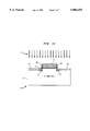
Referring now to FIG. 2, in accordance with one embodiment of the invention, a P-type silicon substrate 12 is covered by a thin silicon oxide layer 14 (gate oxide). The thin silicon oxide layer ranges in thickness from 70 to 300 Angstroms, and functions as the gate dielectric. Other materials may also be used for the gate dielectric. Illustratively, the gate dielectric may be formed by thermal oxidation or chemical vapor deposition (CVD).
A layer of polysilicon 16 is deposited on the thin silicon oxide layer 14 by chemical vapor deposition (CVD). The polysilicon layer 16 ranges in thickness from 1500 to 5000 angstroms. The polysilicon layer is then doped with phosphorous oxychloride (POCl3) in a temperature range of about 800° to 1000° C. to reduce the resistance of the polysilicon. Illustratively, the polysilicon layer is doped to an impurity concentration of about 1E19 to 1E21/cm**3.
In FIG. 3, a first photoresist mask layer 50 is formed on the polysilicon layer 16. The photoresist mask layer has narrow slit openings 52,54.
In FIG. 4, the uncovered regions of the polysilicon layer 16 are etched away. Anisotropic etching is utilized with an etching gas of high selectivity such as hydrogen bromide (HBr/Cl2 /O2). That is, the etching rate is very high for silicon but very low for silicon oxide. As a result, the thin silicon oxide layer 14 acts as an etching stop that protects the silicon substrate from damage during the polysilicon etching process. A gate region 20 is defined in the polysilicon layer 16 between the slit openings 52, 54. Illustratively, the gate electrode region 20 has a width of approximately 0.25 to 0.80 microns and the slit openings 52, 54 have a width of approximately 0.1 to 0.4 microns.
In FIG. 5, the photoresist mask 50 is removed. A first ion implantation 60 is performed to implant N- regions 62, 64 in the silicon substrate below the exposed portions of the thin silicon oxide layer 14. Illustratively, phosphorous ions may be used with an energy of about 5 to 70 kev and a dosage of about 1E13 to 6E13/cm**2. The N- regions 62, 64 illustratively have a depth of approximately 0.05 to 0.5 microns and a doping concentration of about 1E17 to 1E19/cm**3. The first ion implantation takes place through the narrow slit openings. Thus, the lightly doped regions 62, 64 have approximately the same widths as the slits, i.e., 0.1 to 0.4 microns. Thus, the region of the substrate which has primary crystalline defect damage is much smaller than when the above-described conventional NMOSFET formation process is used.
In FIG. 6, a second photoresist mask layer 70 is formed and patterned, only the gate region 20 is covered by the remaining photoresist mask layer 70.
In FIG. 7, the exposed portions of the polysilicon layer 16 are etched away. Anisotropic etching is introduced with an etching gas of high selectivity such as hydrogen bromide (HBr/Cl2 /O2). That is, the etching rate is very high for silicon but very low for silicon oxide. As a result, the thin silicon oxide layer 14 acts as an etching stop that protects the silicon substrate from damage during the polysilicon etching process.
In FIG. 8, photoresist mask is removed.
In FIG. 9, a layer of undoped silicon oxide 26 is deposited on all exposed surface areas to a thickness in the range of about 800 to 3000 angstroms by chemical vapor deposition (CVD). Illustratively, the reacting gas may be SiH2 Cl2 /N2 O, SiH4 /O2 or TEOS/O2, at a temperature in the range of about 400° C. to 800° C.
In FIG. 10, using an anisotropic etching process, the undoped silicon oxide layer 26 and the regions of the thin gate oxide 14 that are not covered by the polysilicon gate 20 are etched with a highly selective etching gas until the silicon substrate is exposed. In other words, the etching rate is very high for silicon oxide but very low for silicon. Illustratively, the etching gas may be CHF3 /CF4. Because the etching depth can be controlled by this process, residual amounts of undoped silicon oxide are retained on the vertical edges of the polysilicon gate electrode region 20. These residual undoped silicon oxide regions act as spacers 30.
In FIG. 11, a second ion implantation 21 is performed to implant source/ drain regions 34, 36 in the silicon substrate 12 beneath the exposed substrate areas. Illustratively, arsenic ions may be used with an energy of about 5 to 100 kev and a dosage of about 1E15 to 8E15/cm**2. The source/ drain regions 34, 36 illustratively have a depth of approximately 0.05 to 0.5 microns, a width of approximately 0.5 to 1.5 microns, and a doping concentration of about 1E20 to 1E21/cm**3.
The advantage of the invention is significant. In this invention, the size of the lightly doped regions that are formed by the first ion implantation are reduced and the primary crystalline defect damage will be effectively reduced. The dopant concentration of source/drain regions that are formed by this new technique are almost the same with the dopant concentration of source/drain regions that are formed by the prior art technique since the dosage of the second ion implantation is about two orders of magnitude greater than the dosage of the first ion implantation.
Thus, the final device structure shown in FIG. 11 is substantially the same as the device structure shown in FIG. 1G. It should be noted that the heavily doped regions 34, 36 may overlap at least in part the lightly doped regions 62, 64. Preferably, the heavily doped regions 62, 64 are continuous with the lightly doped regions 34, 36. The portions of the lightly doped regions 62, 64 under the spacers are generally not overlapped by the heavily doped regions 34, 36.
Finally, the above-described embodiments of the invention are intended to be illustratively only. Numerous alternative embodiments of the invention may be devised by those skilled in the art without departing from the spirit and scope of the following claims. In particular, the formation of an NMOSFET in a P-substrate has been disclosed. However, the NMOSFET can also be formed in a P-well formed in an N-substrate. In addition, the inventive method can also be used to form a PMOSFET in which case the conductivity type of each region is reversed.
Claims (2)
1. A method for forming a MOSFET with LDD type source and drain regions comprising the steps of:
(a) forming on a silicon substrate a gate dielectric layer and a polysilicon layer on the gate dielectric layer,
(b) forming a first mask layer on said polysilicon layer, said first mask layer having two spaced apart narrow slit openings, the slits exposing portions of said polysilicon layer,
(c) removing said exposed portions of said polysilicon layer to form two spaced apart narrow slit openings separated by a gate region in said polysilicon layer,
(d) removing said first mask layer,
(e) performing a first ion implantation into said substrate through said slit openings in said polysilicon layer to form two narrow spaced apart lightly doped regions in said substrate, so that primary crystalline defect damage resulting from the first implantation is confined to the narrow lightly doped regions,
(f) forming a second mask layer which covers said gate region,
(g) removing the remainder of said polysilicon layer not covered by said second mask layer,
(h) forming dielectric spacers on the sidewalls of said gate region, and
(i) performing a second ion implantation in the substrate to form heavily doped source/drain regions on either side of the gate region.
2. The method of claim 1 wherein said narrow lightly doped regions in said substrate have a width of 0.1 to 0.4 microns.
Priority Applications (1)
| Application Number | Priority Date | Filing Date | Title |
|---|---|---|---|
| US08/625,874 US5804455A (en) | 1996-04-01 | 1996-04-01 | Reduced primary crystalline defect damage in NMOSFETS with an optimized LDD structure |
Applications Claiming Priority (1)
| Application Number | Priority Date | Filing Date | Title |
|---|---|---|---|
| US08/625,874 US5804455A (en) | 1996-04-01 | 1996-04-01 | Reduced primary crystalline defect damage in NMOSFETS with an optimized LDD structure |
Publications (1)
| Publication Number | Publication Date |
|---|---|
| US5804455A true US5804455A (en) | 1998-09-08 |
Family
ID=24507980
Family Applications (1)
| Application Number | Title | Priority Date | Filing Date |
|---|---|---|---|
| US08/625,874 Expired - Lifetime US5804455A (en) | 1996-04-01 | 1996-04-01 | Reduced primary crystalline defect damage in NMOSFETS with an optimized LDD structure |
Country Status (1)
| Country | Link |
|---|---|
| US (1) | US5804455A (en) |
Cited By (1)
| Publication number | Priority date | Publication date | Assignee | Title |
|---|---|---|---|---|
| US20060046518A1 (en) * | 2004-08-31 | 2006-03-02 | Micron Technology, Inc. | Method of increasing deposition rate of silicon dioxide on a catalyst |
Citations (8)
| Publication number | Priority date | Publication date | Assignee | Title |
|---|---|---|---|---|
| US4994404A (en) * | 1989-08-28 | 1991-02-19 | Motorola, Inc. | Method for forming a lightly-doped drain (LDD) structure in a semiconductor device |
| JPH03198350A (en) * | 1989-12-26 | 1991-08-29 | Victor Co Of Japan Ltd | Manufacture of ldd structure mos type transistor |
| US5145797A (en) * | 1990-01-30 | 1992-09-08 | Seiko Instruments, Inc. | Method of making semiconductor devices having an implant damage protection film on the gate electrode sidewalls |
| US5200352A (en) * | 1991-11-25 | 1993-04-06 | Motorola Inc. | Transistor having a lightly doped region and method of formation |
| US5374574A (en) * | 1993-11-23 | 1994-12-20 | Goldstar Electron Co., Ltd. | Method for the fabrication of transistor |
| US5384268A (en) * | 1993-01-22 | 1995-01-24 | United Microelectronics Corporation | Charge damage free implantation by introduction of a thin conductive layer |
| US5436176A (en) * | 1990-03-27 | 1995-07-25 | Matsushita Electric Industrial Co., Ltd. | Method for fabricating a semiconductor device by high energy ion implantation while minimizing damage within the semiconductor substrate |
| US5571737A (en) * | 1994-07-25 | 1996-11-05 | United Microelectronics Corporation | Metal oxide semiconductor device integral with an electro-static discharge circuit |
-
1996
- 1996-04-01 US US08/625,874 patent/US5804455A/en not_active Expired - Lifetime
Patent Citations (8)
| Publication number | Priority date | Publication date | Assignee | Title |
|---|---|---|---|---|
| US4994404A (en) * | 1989-08-28 | 1991-02-19 | Motorola, Inc. | Method for forming a lightly-doped drain (LDD) structure in a semiconductor device |
| JPH03198350A (en) * | 1989-12-26 | 1991-08-29 | Victor Co Of Japan Ltd | Manufacture of ldd structure mos type transistor |
| US5145797A (en) * | 1990-01-30 | 1992-09-08 | Seiko Instruments, Inc. | Method of making semiconductor devices having an implant damage protection film on the gate electrode sidewalls |
| US5436176A (en) * | 1990-03-27 | 1995-07-25 | Matsushita Electric Industrial Co., Ltd. | Method for fabricating a semiconductor device by high energy ion implantation while minimizing damage within the semiconductor substrate |
| US5200352A (en) * | 1991-11-25 | 1993-04-06 | Motorola Inc. | Transistor having a lightly doped region and method of formation |
| US5384268A (en) * | 1993-01-22 | 1995-01-24 | United Microelectronics Corporation | Charge damage free implantation by introduction of a thin conductive layer |
| US5374574A (en) * | 1993-11-23 | 1994-12-20 | Goldstar Electron Co., Ltd. | Method for the fabrication of transistor |
| US5571737A (en) * | 1994-07-25 | 1996-11-05 | United Microelectronics Corporation | Metal oxide semiconductor device integral with an electro-static discharge circuit |
Non-Patent Citations (2)
| Title |
|---|
| S. Wolf, R.N. Tauber, Silicon Processing for the VLSI Era , Lattice Press, pp. 295 308, 1996. * |
| S. Wolf, R.N. Tauber, Silicon Processing for the VLSI Era, Lattice Press, pp. 295-308, 1996. |
Cited By (5)
| Publication number | Priority date | Publication date | Assignee | Title |
|---|---|---|---|---|
| US20060046518A1 (en) * | 2004-08-31 | 2006-03-02 | Micron Technology, Inc. | Method of increasing deposition rate of silicon dioxide on a catalyst |
| US20060110936A1 (en) * | 2004-08-31 | 2006-05-25 | Micron Technology, Inc. | Method of increasing deposition rate of silicon dioxide on a catalyst |
| US8110891B2 (en) * | 2004-08-31 | 2012-02-07 | Micron Technology, Inc. | Method of increasing deposition rate of silicon dioxide on a catalyst |
| US8158488B2 (en) | 2004-08-31 | 2012-04-17 | Micron Technology, Inc. | Method of increasing deposition rate of silicon dioxide on a catalyst |
| US8470686B2 (en) | 2004-08-31 | 2013-06-25 | Micron Technology, Inc. | Method of increasing deposition rate of silicon dioxide on a catalyst |
Similar Documents
| Publication | Publication Date | Title |
|---|---|---|
| US4717683A (en) | CMOS process | |
| US5438009A (en) | Method of fabrication of MOSFET device with buried bit line | |
| EP0193117B1 (en) | Method of manufacturing semiconductor device | |
| US6060345A (en) | Method of making NMOS and PMOS devices with reduced masking steps | |
| US5372957A (en) | Multiple tilted angle ion implantation MOSFET method | |
| US5770485A (en) | MOSFET device with an amorphized source and fabrication method thereof | |
| US7795679B2 (en) | Device structures with a self-aligned damage layer and methods for forming such device structures | |
| JP2957757B2 (en) | Transistor fabrication method | |
| US6440805B1 (en) | Method of forming a semiconductor device with isolation and well regions | |
| JP4489467B2 (en) | Method for forming semiconductor device | |
| KR100203131B1 (en) | A method for forming super low junction of semiconductor device | |
| US8120109B2 (en) | Low dose super deep source/drain implant | |
| GB2322005A (en) | Semiconductor device and manufacturing method of the same | |
| JP2802263B2 (en) | Method for manufacturing semiconductor device | |
| US7253054B2 (en) | One time programmable EPROM for advanced CMOS technology | |
| KR100821494B1 (en) | Process for the fabrication of dual gate structures for CMOS devices | |
| US20030111689A1 (en) | Process for the selective formation of salicide on active areas of MOS devices | |
| US20020009847A1 (en) | Semiconductor device, and manufacturing method of the same | |
| US5804455A (en) | Reduced primary crystalline defect damage in NMOSFETS with an optimized LDD structure | |
| JPH09219520A (en) | Transistor and manufacture thereof | |
| US6110788A (en) | Surface channel MOS transistors, methods for making the same, and semiconductor devices containing the same | |
| US5923984A (en) | Method of making enhancement-mode and depletion-mode IGFETS with different gate materials | |
| JPH0147016B2 (en) | ||
| TW563188B (en) | Semiconductor device and method of manufacturing the same | |
| JP3063276B2 (en) | Method for manufacturing semiconductor device |
Legal Events
| Date | Code | Title | Description |
|---|---|---|---|
| AS | Assignment |
Owner name: WINBOND ELECTRONICS CORPORATION, TAIWAN Free format text: ASSIGNMENT OF ASSIGNORS INTEREST;ASSIGNOR:LIU, MING-HSI;REEL/FRAME:008005/0292 Effective date: 19960422 |
|
| STCF | Information on status: patent grant |
Free format text: PATENTED CASE |
|
| FPAY | Fee payment |
Year of fee payment: 4 |
|
| FEPP | Fee payment procedure |
Free format text: PAYOR NUMBER ASSIGNED (ORIGINAL EVENT CODE: ASPN); ENTITY STATUS OF PATENT OWNER: LARGE ENTITY |
|
| FPAY | Fee payment |
Year of fee payment: 8 |
|
| FPAY | Fee payment |
Year of fee payment: 12 |