US5777841A - Method of qualification testing of DC-DC converters - Google Patents
Method of qualification testing of DC-DC converters Download PDFInfo
- Publication number
- US5777841A US5777841A US08/813,263 US81326397A US5777841A US 5777841 A US5777841 A US 5777841A US 81326397 A US81326397 A US 81326397A US 5777841 A US5777841 A US 5777841A
- Authority
- US
- United States
- Prior art keywords
- converters
- testing
- tested
- certain number
- test
- Prior art date
- Legal status (The legal status is an assumption and is not a legal conclusion. Google has not performed a legal analysis and makes no representation as to the accuracy of the status listed.)
- Expired - Lifetime
Links
Images


Classifications
-
- G—PHYSICS
- G01—MEASURING; TESTING
- G01R—MEASURING ELECTRIC VARIABLES; MEASURING MAGNETIC VARIABLES
- G01R31/00—Arrangements for testing electric properties; Arrangements for locating electric faults; Arrangements for electrical testing characterised by what is being tested not provided for elsewhere
- G01R31/40—Testing power supplies
-
- G—PHYSICS
- G01—MEASURING; TESTING
- G01R—MEASURING ELECTRIC VARIABLES; MEASURING MAGNETIC VARIABLES
- G01R31/00—Arrangements for testing electric properties; Arrangements for locating electric faults; Arrangements for electrical testing characterised by what is being tested not provided for elsewhere
- G01R31/003—Environmental or reliability tests
Definitions
- the present invention relates to a method of qualification testing of DC--DC converters.
- DC--DC converters which are an integral and critical component of the telecommunications products, are the key interface between the incoming battery feed voltage and the complex electronics that make up today's telecommunication products. Reliable converters are necessary to ensure the lowest cost of system maintenance and the least possible customer service impact in the telecommunications environment. Many of the DC--DC converters utilized in the telecommunications products are standard commercial units, available from a wide variety of suppliers.
- DC--DC converters The selection of original equipment manufactured (OEM) devices such as DC--DC converters was based on suitability to the desired application. Qualification was granted based on data provided by the supplier which showed evidence that the device in question would comply to the specifications of the product manufacturer. Variables that can influence reliability, but were not assessed in an early approach, include component tolerance variation, design fault, manufacturing process control and human error. DC--DC converter reliability has long been an issue of concern at manufacturers of telecommunication products. Significant numbers of system failures, both in manufacturing and in the field, are due to failures of these devices. In response to these failures, a process to evaluate and qualify DC--DC converters is necessary.
- OEM original equipment manufactured
- a method of qualification testing of a group of DC--DC converters comprising the steps of: (1) testing operation performance of all of the DC--DC converters in the group, under condition of normal temperature; (2) testing thermal coefficients of expansion of a certain number of the DC--DC converters tested at step (1), upon application of thermal shock; (3) testing functionality of a certain number of the DC--DC converters tested at step (2), upon application of power and thermal cycling; (4) testing design margin of a certain number of the DC--DC converters tested at step (2), under step changes in temperature; and (5) performing analysis using capability ratios to determine whether the failures of the group of the DC--DC converters are failed to be qualified, on the basis of short term and mid term capability ratios which are defined by upper and lower specification limits, mean and standard deviation.
- step (5) comprises the step of determining if the mid term capability ratio is less than a predetermined value, the group of the DC--DC converters will be failed.
- the predetermined value of the mid term capability ratio is 1.33.
- the mid term capability ratio Cpk is given by:
- USL, LSL, ⁇ and ⁇ are the upper specification limit, the lower specification limit, the mean and the standard deviation, respectively.
- FIG. 1 is a block diagram of a characterization test platform
- FIG. 2 illustrates a standard test process
- FIG. 3 illustrates a typical power/thermal cycle
- FIG. 4 illustrates a typical step stress cycle
- FIG. 5 illustrates key characterization measurement points
- FIG. 6 illustrates examples of short term capability ratio Cp summary
- FIG. 7 illustrates examples of summary graph for input current deviation
- FIG. 8 illustrates examples of performance graph
- FIG. 9A illustrates distribution histogram at initial test
- FIG. 9B illustrates distribution histogram at final test
- FIG. 10 is a flowchart of a testing process.
- the fixturing method had to mesh the requirements of the qualification program with the generic characteristics of DC--DC converters as listed below.
- FIG. 1 illustrates the typical implementation of fixturing for room temperature characterization.
- a computer 110 is HP (trademark) 3000
- a power supply 112 is HP 6655A
- an electronic load 114 is HP 6050A
- a multi-channel digital voltmeter 116 is Fluke (trademark) Data Bucket.
- a mother board 118 is arranged with a daughter board 120. Similar approaches are used for all other required test platforms.
- the daughter board 120 is designed for each new DC--DC converter footprint.
- One converter is wave soldered directly to each board, ensuring reliable connection to the device terminals.
- Input and output connections to the daughter board 120 are made through high current capacity connectors. It is assumed that all types of DC--DC converters have one primary output which will deliver a higher current output relative to the other two outputs (for triple output types). Since voltage loss in the primary output load path can be significant due to the high current in the higher wattage devices, provision was made for isolated voltage measurement sense lines to be brought directly up to the primary output terminals of the converter through separate connector pins. These sense lines allow voltage measurements to be made at the terminal pins of the device, ensuring highly accurate and repeatable data. Measurements of the input voltage line and auxiliary output voltage lines are sensed on the mother board side of the connector, since the currents in these lines 122 1 , 122 2 ; and 124 1 -124 4 are significantly lower than the primary output.
- the mother board 118 is designed to accommodate up to five daughter boards. Each of the five positions provide connection points for 3 separate loads. Voltage measurement sense lines for the all 3 output voltages and input voltage are fed to a separate connector on segregated lines, again to eliminate any voltage drop effects.
- the mother board wiring and setup can be customized to any specific test set up.
- the mother board 118 is connected to the electronic load 114 and the power supply 112, with all input and output currents measured through series current shunts.
- the shunts and voltage sense lines 122 1 , 122 2 ; and 124 1 -124 4 from the mother board 118 are monitored through the multi-channel digital voltmeter 116, which serves as the data recording device as well. Using the method, a stable, accurate and flexible fixturing platform is achieved.
- Programmable test equipment is used under computer control to set the required line and load conditions for any particular test condition and to record the required measurements.
- An automated test sequence is important for a number of reasons. Timing is critical when attempting to gather consistent parametric data. DC--DC converters can dissipate considerable heat at full load conditions. Control components within the devices heat up, causing subtle changes in operating characteristics. To eliminate, or at least reduce the effect this variable has on the relative consistency of repeated measurements, time under test must be identical for all devices at all times. Secondly, a large quantity of data is collected due to the number of parameters that must be monitored, and the number of units under test. This data must be electronically tabulated for analysis purposes. Automated data collection provides a practical method to gather this information. And thirdly, speed of implementation, and accuracy of the test equipment settings is maintained automatically by using computers to set all required test conditions.
- FIG. 2 shows the standard test plan developed for the qualification of DC--DC converters.
- the plan is based on 32 samples, for example, which flow through various test streams.
- the test process has evolved over time to address not only the application of environmental stresses as a means to identify latent defects, but also to verify operation of the device in accordance with specifications.
- the practical implementation of this process has certain limitations. Ideally, for statistical validity, sample size should be larger. However, individual device cost and the impracticality of processing a larger sample size is prohibitive.
- only the key parameters are measured throughout the program. In order to measure every possible operational parameter (i.e., line and load transient response), time to implement the program would increase from weeks to months.
- the devices to be tested are mounted to test cards and exposed to a standard wave solder process. This eases the assembly operation, but more importantly reproduces the thermal shock the devices would see in a typical manufacturing process.
- An initial room temperature characterization is then performed an all samples. This derives the initial baseline data that will be used for comparative analysis, and also verifies "out of the box" performance. Failures have been encountered at this early stage, whether due to the wave solder stress or due to a non functional unit shipped from the supplier. Room temperature characterization is repeated at various points in the test process in order to test for non functional devices and to obtain additional data which will be used in the analysis process.
- Thermal shock is applied to unpowered units using an air-to-air elevator style environmental chamber.
- This style of chamber has long been used to perform MIL STD 202 type thermal cycling on integrated circuits.
- the specified storage temperature limits of the device are used to derive the upper and lower limits of this test.
- the objective of this test is to induce the maximum possible change in temperature and rate of change of temperature on the devices under test (DUT).
- materials such as fiberglass, plastics, solder, copper, aluminum and glass used in construction of the DC--DC converters will have different thermal coefficients of expansion (TCEs), can be exploited using thermal shock to precipitate defects. Repetitive cycling between temperature extremes will maximize the relative expansion and contraction between these different material interfaces. Poor solder adhesion, improper wire bonding and other types of material interface defects are quickly revealed using this technique.
- FIG. 3 illustrates a typical power/thermal power cycle. Limits of temperature and voltage applied during the power/thermal cycling test are determined based on the published performance specifications of the supplier. Case operating temperatures are varied between the published upper and lower operating temperature limits. Input voltages are varied between minimum, maximum, nominal and zero. Typically, each temperature plateau is 20 minutes long, and power is cycled on and off at a rate of 60 seconds. These times are chosen to allow sufficient equalization time at the temperature plateaus, while maximizing the number of power cycles applied.
- Powering the device introduces a current inrush stress and voltage stress, and verifies operation at the combined extremes of temperature, input voltage and output load. These additional stresses reveal functional defects. Typical problems found during power/thermal cycling include failure to startup, output voltage drift, and inability to withstand multiple inrush current surges. These problems relate to poor design margins and limitations with component derating for temperature, current or voltage.
- Biased humidity is used to verify the absence of corrosive fluxes or other contaminants introduced during the manufacturing process. This is especially important for potted devices. Potting can be used to hide various manufacturing flaws, such as poor workmanship or process flaws. To check for such flaws, the devices are initially soaked for 24 hours in an unpowered mode. Maximum voltage is then applied on a cycled basis, 10 seconds on, 10 seconds off. The output is loaded to the absolute minimum amount required to keep the converter in stable operation. These test parameters are designed to prevent or minimize self heating of the converters so that local moisture does not burn off. Failures typically manifest as minor changes in input current, either during the exposure or afterwards at room temperature characterization.
- Step stress testing uncovers limitations in design, workmanship, component selection and operational margins that are often missed by other evaluation methods. Verification of design margin ensures that the device will be able to withstand the normal manufacturing process fluctuations, component tolerance variations, component substitutions and staff training variables that occur in a manufacturing environment. At the same time it ensures the device meets and in some cases exceeds its specified requirements and remains reliable.
- the process involves subjecting the device t o increasing environmental and electrical stresses, up to the limits of the technology.
- a limit of technology is defined as a parameter that will cause failure once exceeded, such as the maximum junction temperature of a power semiconductor.
- Step stressing begins by ex posing the device to step changes in temperature from ambient up to and beyond the specified operating limits of the device. At each step the same parameters tested during room temperature characterization are monitored. Cold operation is tested, then hot, up to the point where the device is no longer operating correctly or has failed altogether. Once temperature operating limits have been evaluated, the stresses of random vibration, rapid thermal cycling and input power cycling are combined in a simultaneous fashion to accumulate a level of repetitive fatigue on the device (FIG. 4). As in power/thermal cycling, each temperature plateau is 20 minutes long, and power is cycled on and off at a rate of 60 seconds. Output load is alternated between minimum and maximum every 30 seconds. Vibration is applied for 10 minutes at each temperature plateau. The combination of these stresses will often precipitate hidden flaws that might go undetected under single-stress applications.
- RF and audio rangee missions conducted back to input supply are measured. These measurements do not relate to reliability or robustness, but are important to obtain early in the system design cycle. Conducted emissions of the converter must be known, so that proper filtering can be incorporated into the system design where the converter is to be used. If characterization for conducted emissions was left to the final stage, the system may fail to meet certain regulatory requirements, resulting in costly time delays and redesign. The qualification stage is an ideal point to gather the required data, which can be fed to system designers.
- a detailed examination of the short circuit protection of the device is performed to verify that such things as thermal runaway or catastrophic failure do not occur.
- This test differs from the short circuit protection test conducted during characterization, which only verifies that the device remains undamaged under a short circuit condition.
- the detailed test more closely examines through observation and measurement the various characteristics of the device under a long term short condition. This test takes significantly longer to apply than the characterization test, and so is conducted separately.
- Failures can manifest in number of ways. For example, there are catastrophic failures, where a device is no longer functional; or failures which are detected through the in-process monitoring of the device, such as a voltage drift or failure to re-start at temperature extremes. These failures are easily detected through observation. However, more subtle faults may be indicated by small shifts in parametric data. The shift may be so minor that the particular parameter in question can still appear to be within specification. These faults are termed soft failures, and are detected through analysis of the data using a number of methods. Several of the analysis techniques discussed in this section provide overlapping results. This is considered necessary to corroborate findings. Since the faults that are being detected are the outcome of very minor parametric shifts, more than one analysis approach provides greater confidence. This is especially important when raising issues based on data that may still be within specification.
- each of the 32 samples are characterized at room temperature. This tests the response of the devices for all critical functions, at all possible conditions of input voltage and output load. The most useful data gained from these tests are input current and output voltage, which are the key operational variables (since input voltage and output current are defined by the test condition). From these values, efficiency is calculated as well. Therefore, six values for input current, output voltage and efficiency are derived for each of the 32 test samples during each characterization, as illustrated in FIG. 5.
- All characterization data is tabulated into tables specific to each test condition.
- a typical analysis spreadsheet for a single output device contains 23 tables; 6 each for efficiency, input current, output voltage, and 5 additional tables for startup voltage, shutdown voltage, short circuit protection, and line/load regulation.
- a typical table of data is represented in Table II.
- the data is analyzed in two ways; looking across at the variation of repeated measurements for the same sample number (x), and looking down at the distribution of measurements relative to the complete sample lot (y).
- the desired outcome of all analysis is the same, to highlight any device which has undergone a shift in operating parameters.
- the short term capability ratio Cp and the mid term capability ratio Cpk are statistical representations of the capability of any given process (i.e., the actual measured distribution) relative to the specified or calculated limits (i.e., the mean, upper and lower specification limits).
- the short term capability ratio Cp is the ratio of the measured distribution relative to the specification width.
- the mid term capability ratio Cpk is an indication (expressed as a ratio) of the centering of data relative the specified mean value.
- the short term capability ratio Cp and the mid term capability ratio Cpk are determined using the following formulas:
- the mid term capability ratio Cpk (Ya in Table II) provides an indicator of the spread of data relative to a given set of upper and lower limits and is useful for determining if any shifts have taken place during the test program. This would be indicated by a drop in value for short term capability ratio Cp relative to the initial value.
- the mid term capability ratio Cpk (Yb in Table II) provides an indicator of how well centered the data is to a nominal mean value and indicates things such as poor design centering, lack of process control, poor quality components, or that some critical parameter has changed over the course of testing.
- a high value for the short term and mid term capability ratios Cp and Cpk indicates that all devices were initially well centered to the nominal mean value, and that the distribution was tight.
- Standard deviation is used to detect parametric variation of a repeated measurement for the same sample number, shown as x b in Table II. These values are plotted on a summary graph for all six line and load conditions to provide a clear visual indication of fault. Any unit displaying a high value for standard deviation relative to the other samples is considered questionable, and a candidate for full root cause analysis. It is important to plot all six line and load conditions.
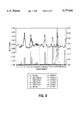
- FIG. 7 illustrates how the magnitude of error can be much more pronounced at specific conditions. The high peaks seen at maximum input voltage/minimum load in FIG. 7 are units which suffered cracked transformer cores during the test program. This is a clear example of failure detection that would have been missed had not all operational conditions been tested and analyzed.
- the magnitude of the problem can be identified by examining a performance graph (FIG. 8). For example, the data in FIG. 6 indicates that the distribution spread of the test lot has increased during test.
- FIG. 7 indicates input current values of a number of units fluctuated, but does not give an indication of trend.
- the specific fault conditions can be identified by viewing a plot of the individual unit parameters. This plot provides a visual indicator of the trend and degree of the fault condition, and highlights units which may have drifted over time, as well as units which are significantly different as compared to the rest of the lot. Standard deviation is also plotted as a visual pointer. Any unit which has a high bar for standard deviation is considered suspect and returned to the supplier for full root cause analysis.
- Histograms for efficiency, output voltage and input current are plotted as a final check, and assist in finding suspect "outliers", units which are significantly outside the normal distribution. Once again, the focus is to highlight any unit which has either shifted in performance, or is significantly different as compared to the test lot. Even if the parameter in question is within specification, the unit is still considered suspect because of it's variation from other units and returned for full root cause analysis. Histograms are plotted using the initial and final characterization data and compared as shown in FIGS. 9A and 9B.
- a detailed failure analysis and identification of root causes for correction is critical to the effectiveness of any product qualification program.
- the qualification program must run as a closed loop, so that any reliability issues precipitated by this testing are identified and proper corrective actions implemented.
- the supplier of DC--DC converters is responsible for this key function, and must perform the failure analysis and implement any appropriate changes.
- the supplier is asked the following basic questions; what failed, why did it fail, and what can be done to correct it. Often, care must be taken to ensure that the supplier performs a sufficiently detailed analysis and has adequately identified the root cause of the problem. For example, what could appear as a random component failure on initial examination could in fact be due to a particular component specification that was not adhered to. Occasionally, it is necessary to conduct failure analysis as a joint effort, with manufacturer's offering failure analysis lab facilities and expertise, and the manufacturer providing the design guidance. Full root cause analysis must look at all possible aspects related to the failure, such as design tolerance, process control, component lot variation, etc.
- FIG. 10 An entire process of the qualification testing of dc--dc converters is shown in FIG. 10. Referring to FIG. 10, each step of the process will be described below.
- Room temperature measurements of the devices are collected for key electrical parameters (input current, output voltage, startup voltage, shutdown voltage, short circuit current) as received from the supplier. All measurements are recorded electronically and tabulated in an Excel spreadsheet file. These initial measurements are used as a baseline, and are compared against later measurements for deltas (see Section III. Test Process, "A. Initial Characterization Test").
- the devices are exposed to operational stress in the form of temperature cycling, input voltage cycling, output load cycling, vibration cycling and humidity exposure. These stresses are used to simulate extreme operating conditions so that an accelerated operating time period is achieved. At the same time, these stresses are not considered so excessive as to cause a device to fail, except in the case of step stress testing, which intentionally exceeds operating specification limits. All devices, with the exception of those exposed to step stress testing are expected to survive exposure to stress with no deviation in operating characteristics. Measurements data is collected and recorded on all tests involving active biasing of the device (see Section "III. Test Process”, “B. Thermal Shock Test”, “C. Power/Thermal Cycling Test”, “D. Humidity Exposure Test” and “E. Step Stress Test”.
- Step 3 Analyze Data Measured During Stress
- the data is anlayzed for centering and spread of the sample population relative to NPS specified limits using the short term and mid term capability ratios Cp and Cpk calculations (see Section "V. Failure Analysis”, “A. Distribution Analysis” and “C. Performance Graphs”).
- Step 7 Statistical Outliers
- Standard deviation is calculated for repeated measurements. High standard deviation indicates a variable reading or change in reading over the course of the test program (see Section "V. Failure Analysis”, “B. Parametric Variation Analysis” and “C. Performance Graphs”).
- the above described method is an effective method to evaluate the robustness and reliability of DC--DC converters from various suppliers in a cost effective and timely matter.
Landscapes
- Physics & Mathematics (AREA)
- General Physics & Mathematics (AREA)
- Engineering & Computer Science (AREA)
- Environmental & Geological Engineering (AREA)
- Testing Of Individual Semiconductor Devices (AREA)
Abstract
Description
Cpk=min (USL-μ/3σ), ( μ-LSL/3σ)!
              TABLE I
______________________________________
Types of Defects Detected vs. Applied Stresses
                         Power/  Step
                 Thermal Thermal Stress
                                      Biased
Defect or Root Cause
                 Shock   Cycling Test Humidity
______________________________________
Performance specification drift
                 X       X       X    X
Insufficient solder pad size
                 X       X
Partially nicked transformer wires
                 X       X       X
Incorrect temp range components
                         X       X
Poor soldering caused by heat
                 X       X
sinking
Improper sized conductors
                         X       X
Poor solder paste application
                 X       X
Ionic contamination      X            X
Poor electrical design practices
                         X       X
Improper mechanical fastening
                 X       X       X
Improper wire bonding process
                 X       X       X
Defective components
                 X       X       X    X
Cold solder joints
                 X       X       X
Insufficient design margin
                         X       X
Improper component voltage rating
                         X       X
Excessive output noise           X
Improper part placement
                 X       X       X
______________________________________
TABLE II ______________________________________ Typical Data TableUnit # Test 1Test 2Test 3 etc Mean σ ______________________________________ 1 Val.sub.-- 1.1 Val.sub.-- 1.2 Val.sub.-- 1.3 x.sub.ax.sub.b 2 Val.sub.-- 2.1 Val.sub.-- 2.2 Val.sub.-- 2.3 x.sub.ax.sub.b 3 Val.sub.-- 3.1 Val.sub.-- 3.2 Val.sub.-- 3.3 x.sub.a x.sub.b ↓ ↓ ↓ ↓ ↓ ↓ ↓ 32 Val.sub.-- 32.1 Val.sub.-- 32.2 Val.sub.-- 32.3 ?? x.sub.a x.sub.b Mean y y y y σ y y y y C.sub.p y.sub.a y.sub.a y.sub.a y.sub.a C.sub.pk y.sub.b y.sub.b y.sub.b y.sub.b ______________________________________
Cp=(USL-LSL)/(6σ)
Cpk=min (USL-μ/3σ), (μ-LSL/3σ)!
Claims (12)
Cpk=min (USL-μ/3σ), (μ-LSL/3σ)!
Cpk=min (USL-μ/3σ), (μ-LSL/3σ)!
Priority Applications (1)
| Application Number | Priority Date | Filing Date | Title |
|---|---|---|---|
| US08/813,263 US5777841A (en) | 1997-03-07 | 1997-03-07 | Method of qualification testing of DC-DC converters |
Applications Claiming Priority (1)
| Application Number | Priority Date | Filing Date | Title |
|---|---|---|---|
| US08/813,263 US5777841A (en) | 1997-03-07 | 1997-03-07 | Method of qualification testing of DC-DC converters |
Publications (1)
| Publication Number | Publication Date |
|---|---|
| US5777841A true US5777841A (en) | 1998-07-07 |
Family
ID=25211917
Family Applications (1)
| Application Number | Title | Priority Date | Filing Date |
|---|---|---|---|
| US08/813,263 Expired - Lifetime US5777841A (en) | 1997-03-07 | 1997-03-07 | Method of qualification testing of DC-DC converters |
Country Status (1)
| Country | Link |
|---|---|
| US (1) | US5777841A (en) |
Cited By (16)
| Publication number | Priority date | Publication date | Assignee | Title |
|---|---|---|---|---|
| US6047293A (en) * | 1997-09-16 | 2000-04-04 | Teradyne, Inc. | System for storing and searching named device parameter data in a test system for testing an integrated circuit |
| US6463391B1 (en) * | 1999-12-22 | 2002-10-08 | General Electric Company | Method and apparatus for calculating confidence intervals |
| US6480808B1 (en) * | 1999-12-22 | 2002-11-12 | General Electric Company | Method and apparatus for calculating confidence intervals |
| US6496347B1 (en) * | 2000-03-08 | 2002-12-17 | General Electric Company | System and method for optimization of a circuit breaker mechanism |
| US6631305B2 (en) | 2000-05-03 | 2003-10-07 | General Electric Company | Capability analysis of assembly line production |
| US6788077B2 (en) | 2001-12-20 | 2004-09-07 | Abb Inc. | Automated test sequence editor and engine for transformer testing |
| US7219068B2 (en) | 2001-03-13 | 2007-05-15 | Ford Motor Company | Method and system for product optimization |
| US20070282473A1 (en) * | 2006-06-05 | 2007-12-06 | Oohashi Hiromichi | Method, system and program for designing power converter |
| WO2011044827A1 (en) * | 2009-10-16 | 2011-04-21 | 华为终端有限公司 | Self-diagnosis method and system for wireless data service device |
| CN102621502A (en) * | 2012-03-29 | 2012-08-01 | 首都师范大学 | Fault monitoring and forecasting method of direct current (DC)-direct current (DC) power source system |
| CN102628901A (en) * | 2012-03-30 | 2012-08-08 | 株洲南车时代电气股份有限公司 | Rail transit electrical equipment reliability test method |
| CN107807334A (en) * | 2016-08-31 | 2018-03-16 | 北京飞跃新能科技有限公司 | Method of testing and device |
| US10718820B2 (en) * | 2017-03-03 | 2020-07-21 | Boe Technology Group Co., Ltd. | DC/DC test system and method |
| CN114460395A (en) * | 2021-12-31 | 2022-05-10 | 锐凌无线有限责任公司 | Test method of wireless communication module |
| CN115032474A (en) * | 2021-12-31 | 2022-09-09 | 中国空间技术研究院 | Novel anti-radiation DC/DC converter characteristic characterization method |
| CN115792471A (en) * | 2023-01-29 | 2023-03-14 | 深圳市创世富尔电子有限公司 | Electronic transformer testing method and device, computer equipment and storage medium |
Citations (4)
| Publication number | Priority date | Publication date | Assignee | Title |
|---|---|---|---|---|
| US4932075A (en) * | 1986-07-03 | 1990-06-05 | Hughes Aircraft Company | High speed wide range variable rate power detector |
| US5390129A (en) * | 1992-07-06 | 1995-02-14 | Motay Electronics, Inc. | Universal burn-in driver system and method therefor |
| US5414341A (en) * | 1993-12-07 | 1995-05-09 | Benchmarq Microelectronics, Inc. | DC-DC converter operable in an asyncronous or syncronous or linear mode |
| US5470341A (en) * | 1993-12-10 | 1995-11-28 | Medtronic, Inc. | High voltage switch drive for implantable cardioverter/defibrillator |
-
1997
- 1997-03-07 US US08/813,263 patent/US5777841A/en not_active Expired - Lifetime
Patent Citations (4)
| Publication number | Priority date | Publication date | Assignee | Title |
|---|---|---|---|---|
| US4932075A (en) * | 1986-07-03 | 1990-06-05 | Hughes Aircraft Company | High speed wide range variable rate power detector |
| US5390129A (en) * | 1992-07-06 | 1995-02-14 | Motay Electronics, Inc. | Universal burn-in driver system and method therefor |
| US5414341A (en) * | 1993-12-07 | 1995-05-09 | Benchmarq Microelectronics, Inc. | DC-DC converter operable in an asyncronous or syncronous or linear mode |
| US5470341A (en) * | 1993-12-10 | 1995-11-28 | Medtronic, Inc. | High voltage switch drive for implantable cardioverter/defibrillator |
Non-Patent Citations (5)
| Title |
|---|
| Abstract by Ellacott, Ken "Practical test method for DC-DC Converter qualification", Proceedings of 1996 IEEE 46th Electronic Components & Technology Conference, ECTC May 28, 1996. |
| Abstract by Ellacott, Ken Practical test method for DC DC Converter qualification , Proceedings of 1996 IEEE 46th Electronic Components & Technology Conference, ECTC May 28, 1996. * |
| Abstract, Ellacott, Ken "Qualification testing of DC-DC converters"; Proceedings of the 1997 IEEE 12th Applied Power Electronics Conference, APEC 97, Feb. 23, 1997. |
| Abstract, Ellacott, Ken Qualification testing of DC DC converters ; Proceedings of the 1997 IEEE 12th Applied Power Electronics Conference, APEC 97, Feb. 23, 1997. * |
| Motorola University, May 1990, entitled Six Sigma Producibility Analysis and Process Characterization by Mikel J. Harry and J. Ronald Lawson. * |
Cited By (21)
| Publication number | Priority date | Publication date | Assignee | Title |
|---|---|---|---|---|
| US6047293A (en) * | 1997-09-16 | 2000-04-04 | Teradyne, Inc. | System for storing and searching named device parameter data in a test system for testing an integrated circuit |
| US6463391B1 (en) * | 1999-12-22 | 2002-10-08 | General Electric Company | Method and apparatus for calculating confidence intervals |
| US6480808B1 (en) * | 1999-12-22 | 2002-11-12 | General Electric Company | Method and apparatus for calculating confidence intervals |
| US6496347B1 (en) * | 2000-03-08 | 2002-12-17 | General Electric Company | System and method for optimization of a circuit breaker mechanism |
| US6631305B2 (en) | 2000-05-03 | 2003-10-07 | General Electric Company | Capability analysis of assembly line production |
| US7219068B2 (en) | 2001-03-13 | 2007-05-15 | Ford Motor Company | Method and system for product optimization |
| US6788077B2 (en) | 2001-12-20 | 2004-09-07 | Abb Inc. | Automated test sequence editor and engine for transformer testing |
| US20070282473A1 (en) * | 2006-06-05 | 2007-12-06 | Oohashi Hiromichi | Method, system and program for designing power converter |
| US7599754B2 (en) * | 2006-06-05 | 2009-10-06 | National Institute Of Advanced Industrial Science And Technology | Method and system for designing a power converter |
| WO2011044827A1 (en) * | 2009-10-16 | 2011-04-21 | 华为终端有限公司 | Self-diagnosis method and system for wireless data service device |
| CN102621502A (en) * | 2012-03-29 | 2012-08-01 | 首都师范大学 | Fault monitoring and forecasting method of direct current (DC)-direct current (DC) power source system |
| CN102621502B (en) * | 2012-03-29 | 2016-09-14 | 首都师范大学 | A kind of DC-DC power source system failure monitoring and Forecasting Methodology |
| CN102628901A (en) * | 2012-03-30 | 2012-08-08 | 株洲南车时代电气股份有限公司 | Rail transit electrical equipment reliability test method |
| CN102628901B (en) * | 2012-03-30 | 2014-11-12 | 株洲南车时代电气股份有限公司 | Rail transit electrical equipment reliability test method |
| CN107807334A (en) * | 2016-08-31 | 2018-03-16 | 北京飞跃新能科技有限公司 | Method of testing and device |
| CN107807334B (en) * | 2016-08-31 | 2024-02-09 | 北京飞跃新能科技有限公司 | Test method and device |
| US10718820B2 (en) * | 2017-03-03 | 2020-07-21 | Boe Technology Group Co., Ltd. | DC/DC test system and method |
| CN114460395A (en) * | 2021-12-31 | 2022-05-10 | 锐凌无线有限责任公司 | Test method of wireless communication module |
| CN115032474A (en) * | 2021-12-31 | 2022-09-09 | 中国空间技术研究院 | Novel anti-radiation DC/DC converter characteristic characterization method |
| CN115792471A (en) * | 2023-01-29 | 2023-03-14 | 深圳市创世富尔电子有限公司 | Electronic transformer testing method and device, computer equipment and storage medium |
| CN115792471B (en) * | 2023-01-29 | 2023-04-28 | 深圳市创世富尔电子有限公司 | Electronic transformer testing method, device, computer equipment and storage medium |
Similar Documents
| Publication | Publication Date | Title |
|---|---|---|
| US5777841A (en) | Method of qualification testing of DC-DC converters | |
| EP1479025B1 (en) | Methods and apparatus for semiconductor testing | |
| US5030905A (en) | Below a minute burn-in | |
| US6441637B1 (en) | Apparatus and method for power continuity testing in a parallel testing system | |
| US7324982B2 (en) | Method and apparatus for automated debug and optimization of in-circuit tests | |
| US5363048A (en) | Method and system for ensuring interconnect integrity in a micro-chip-module | |
| Cooper | Introduction to HALT-making your product robust | |
| Natarajan | Reliable Design of Electronic Equipment | |
| US6311301B1 (en) | System for efficient utilization of multiple test systems | |
| Ellacott | Qualification testing of DC-DC converters | |
| US6101458A (en) | Automatic ranging apparatus and method for precise integrated circuit current measurements | |
| JP2822999B2 (en) | High temperature defect sorting apparatus and high temperature defect sorting method | |
| US6114181A (en) | Pre burn-in thermal bump card attach simulation to enhance reliability | |
| US5570012A (en) | Apparatus for testing a semiconductor device by comparison with an identical reference device | |
| Gralian | Next generation burn-in development | |
| Ellacott et al. | A practical test method for DC-DC converter qualification | |
| KR100801629B1 (en) | Inspection and maintenance of nuclear power plant electronic circuit board | |
| Vartiainen | Mapping of the Test Coverage of Function Module Tester | |
| Prakash | The application of HALT and HASS principles in a high‐volume manufacturing environment | |
| Abillar et al. | Development and implementation of a board checker for fast loop circuitry in testing microelectronic packages | |
| Teverovsky | Qualification of PEMs Using Board-level Testing | |
| Kuokka | Use of stress screening in electrical system production quality control | |
| Gupta et al. | Reliability Qualification Challenges and Flow for Analog Qualification Test Vehicle | |
| Farnholtz | Operational life testing of electronic components | |
| KR100445795B1 (en) | Semiconductor chip test apparatus |
Legal Events
| Date | Code | Title | Description |
|---|---|---|---|
| AS | Assignment |
Owner name: BELL-NORTHERN RESEARCH LTD., CANADA Free format text: ASSIGNMENT OF ASSIGNORS INTEREST;ASSIGNORS:STONE, KEVIN PATRICK;ELLACOTT, KEN DAVID;REEL/FRAME:008436/0622;SIGNING DATES FROM 19970227 TO 19970303 |
|
| AS | Assignment |
Owner name: NORTHERN TELECOM LIMITED, CANADA Free format text: ASSIGNMENT OF ASSIGNORS INTEREST;ASSIGNOR:BELL-NORTHERN RESEARCH LTD.;REEL/FRAME:008476/0197 Effective date: 19970418 |
|
| STCF | Information on status: patent grant |
Free format text: PATENTED CASE |
|
| AS | Assignment |
Owner name: NORTEL NETWORKS CORPORATION, CANADA Free format text: CHANGE OF NAME;ASSIGNOR:NORTHERN TELECOM LIMITED;REEL/FRAME:010567/0001 Effective date: 19990429 |
|
| AS | Assignment |
Owner name: NORTEL NETWORKS LIMITED, CANADA Free format text: CHANGE OF NAME;ASSIGNOR:NORTEL NETWORKS CORPORATION;REEL/FRAME:011195/0706 Effective date: 20000830 Owner name: NORTEL NETWORKS LIMITED,CANADA Free format text: CHANGE OF NAME;ASSIGNOR:NORTEL NETWORKS CORPORATION;REEL/FRAME:011195/0706 Effective date: 20000830 |
|
| FEPP | Fee payment procedure |
Free format text: PAYOR NUMBER ASSIGNED (ORIGINAL EVENT CODE: ASPN); ENTITY STATUS OF PATENT OWNER: LARGE ENTITY |
|
| FPAY | Fee payment |
Year of fee payment: 4 |
|
| REMI | Maintenance fee reminder mailed | ||
| FPAY | Fee payment |
Year of fee payment: 8 |
|
| SULP | Surcharge for late payment |
Year of fee payment: 7 |
|
| AS | Assignment |
Owner name: INNOVATION MANAGEMENT SCIENCES, LLC, CALIFORNIA Free format text: ASSIGNMENT OF ASSIGNORS INTEREST;ASSIGNOR:NORTEL NETWORKS LIMITED;REEL/FRAME:019215/0788 Effective date: 20070424 |
|
| AS | Assignment |
Owner name: POPKIN FAMILY ASSETS, L.L.C., DELAWARE Free format text: ASSIGNMENT OF ASSIGNORS INTEREST;ASSIGNOR:INNOVATION MANAGEMENT SCIENCES LLC;REEL/FRAME:019605/0022 Effective date: 20070427 |
|
| FEPP | Fee payment procedure |
Free format text: PAYER NUMBER DE-ASSIGNED (ORIGINAL EVENT CODE: RMPN); ENTITY STATUS OF PATENT OWNER: LARGE ENTITY Free format text: PAYOR NUMBER ASSIGNED (ORIGINAL EVENT CODE: ASPN); ENTITY STATUS OF PATENT OWNER: LARGE ENTITY |
|
| FPAY | Fee payment |
Year of fee payment: 12 |
|
| AS | Assignment |
Owner name: BENHOV GMBH, LLC, DELAWARE Free format text: MERGER;ASSIGNOR:POPKIN FAMILY ASSETS L.L.C.;REEL/FRAME:037241/0651 Effective date: 20150811 |
|
| AS | Assignment |
Owner name: HANGER SOLUTIONS, LLC, GEORGIA Free format text: ASSIGNMENT OF ASSIGNORS INTEREST;ASSIGNOR:INTELLECTUAL VENTURES ASSETS 161 LLC;REEL/FRAME:052159/0509 Effective date: 20191206 |
|
| AS | Assignment |
Owner name: INTELLECTUAL VENTURES ASSETS 161 LLC, DELAWARE Free format text: ASSIGNMENT OF ASSIGNORS INTEREST;ASSIGNOR:BENHOV GMBH, LLC;REEL/FRAME:051856/0776 Effective date: 20191126 |