US5765191A - Method for implementing a four-way least recently used (LRU) mechanism in high-performance - Google Patents

Method for implementing a four-way least recently used (LRU) mechanism in high-performance Download PDF

Info

Publication number
US5765191A
US5765191A US08/641,060 US64106096A US5765191A US 5765191 A US5765191 A US 5765191A US 64106096 A US64106096 A US 64106096A US 5765191 A US5765191 A US 5765191A
Authority
US
United States
Prior art keywords
recently used
cache
lru
sets
way
Prior art date
Legal status (The legal status is an assumption and is not a legal conclusion. Google has not performed a legal analysis and makes no representation as to the accuracy of the status listed.)
Expired - Fee Related
Application number
US08/641,060
Inventor
Albert John Loper
Soummya Mallick
Rajesh Bhikhubhai Patel
Michael Putrino
Current Assignee (The listed assignees may be inaccurate. Google has not performed a legal analysis and makes no representation or warranty as to the accuracy of the list.)
International Business Machines Corp
Original Assignee
International Business Machines Corp
Priority date (The priority date is an assumption and is not a legal conclusion. Google has not performed a legal analysis and makes no representation as to the accuracy of the date listed.)
Filing date
Publication date
Application filed by International Business Machines Corp filed Critical International Business Machines Corp
Priority to US08/641,060 priority Critical patent/US5765191A/en
Assigned to INTERNATIONAL BUSINESS MACHINES CORPORATION reassignment INTERNATIONAL BUSINESS MACHINES CORPORATION ASSIGNMENT OF ASSIGNORS INTEREST (SEE DOCUMENT FOR DETAILS). Assignors: LOPER, ALBERT JOHN, MALLICK, SOUMMYA, PATEL, RAJESH BHIKHUBHAI, PUTRINO, MICHAEL
Priority to KR1019970004597A priority patent/KR970071286A/en
Priority to JP10630797A priority patent/JP3239333B2/en
Application granted granted Critical
Publication of US5765191A publication Critical patent/US5765191A/en
Anticipated expiration legal-status Critical
Expired - Fee Related legal-status Critical Current

Links

Images

Classifications

    • GPHYSICS
    • G06COMPUTING; CALCULATING OR COUNTING
    • G06FELECTRIC DIGITAL DATA PROCESSING
    • G06F12/00Accessing, addressing or allocating within memory systems or architectures
    • G06F12/02Addressing or allocation; Relocation
    • G06F12/08Addressing or allocation; Relocation in hierarchically structured memory systems, e.g. virtual memory systems
    • G06F12/12Replacement control
    • G06F12/121Replacement control using replacement algorithms
    • G06F12/123Replacement control using replacement algorithms with age lists, e.g. queue, most recently used [MRU] list or least recently used [LRU] list

Definitions

  • the present disclosure relates to a method for improving data processing in general and, in particular, to a method of implementing a Least Recently Used (LRU) mechanism in a cache memory within a data processing system. Still more particularly, the present disclosure relates to a method for implementing a four-way LRU mechanism in a four-way cache memory within a high-performance data processing system.
  • LRU Least Recently Used
  • a high-performance data processing system typically includes both a system memory and a cache memory.
  • a cache memory is a small and relatively high-speed memory interposed between a processor and the system memory. Information such as data or instruction may be copied from a portion of the system memory into the cache memory so that the information will be available to the processor in a relatively short amount of time.
  • LRU Least Recently Used
  • the implementation of a two-way LRU mechanism in a two-way cache memory is quite trivial in that it requires only one bit of information per cache line.
  • the implementation of a four-way LRU mechanism in a four-way cache memory requires a larger number of bits.
  • Other implementations of the four-way cache memory utilize six bits ((N-1)log 2 N)) to store similar essential information.
  • This disclosure provides a method for implementing the four-way LRU mechanism in a high-performance data processing system with fewer bits than the prior art implementations.
  • LRU Least Recently Used
  • a method of implementing a least recently used cache line replacement scheme in a cache memory having units of information by utilizing less than (N-1)log 2 N bits, where N is the number of units (or congruence sets) within the cache memory is disclosed.
  • the four-way cache memory includes multiple cache lines, and each cache line includes four congruence sets.
  • a five-bit Least Recently Used (LRU) field is associated with each of the cache lines within the cache memory. For a particular cache line, a set number of a least recently used set among the four congruence sets is stored in any two bits of the LRU field associated with that cache line. Next, a set number of the second least recently used set among the four congruence sets is stored in another two bits of the same LRU field associated with the same cache line. Finally, a last bit of the five-bit LRU field is set to a specific state in response to a determination of which one of the remaining two sets is the second most recently used set.
  • LRU Least Recently Used
  • FIG. 1 is a block diagram of an illustrative embodiment of a processor which utilizes the method of the present disclosure
  • FIG. 2 is a block diagram of a cache memory within the processor of FIG. 1, according to an illustrative embodiment of the present disclosure
  • FIG. 3 is a depiction of an example of a true LRU scheme
  • FIG. 4a is an illustration of a prior art implementation of a four-way LRU field by utilizing eight bits
  • FIG. 4b is an illustration of a prior art implementation of a four-way LRU field by utilizing six bits
  • FIG. 5 is an illustration of an implementation of a four-way LRU field according to an illustrative embodiment of the present disclosure.
  • FIG. 6 is a depiction of some examples for illustrating the application of the four-way LRU mechanism according to an illustrative embodiment of the disclosure.
  • An illustrative embodiment under the present disclosure may be implemented on a variety of processors and cache-based data processing systems.
  • an illustrative embodiment as described below is implemented on one of the PowerPCTM line of microprocessors manufactured by International Business Machines Corporation, which operates according to reduced instruction set computing (RISC) techniques.
  • RISC reduced instruction set computing
  • processor 10 is a single integrated circuit superscalar microprocessor, comprising various registers, buffers, execution units, and functional units.
  • processor 10 is coupled to system bus 11 via a bus interface unit (BIU) 12 within processor 10.
  • BIU 12 controls the transfer of information between processor 10 and other devices, such as a main memory (not shown), that are coupled to system bus 11.
  • processor 10 system bus 11, and the other devices coupled to system bus 11 together form a host data processing system.
  • BIU 12 is connected to instruction cache 14 and data cache 16, in both of which an illustrative embodiment of the present disclosure may be incorporated.
  • Both instruction cache 14 and data cache 16 are high-speed caches which enable processor 10 to achieve a relatively fast access time to a subset of instructions or data previously transferred from main memory to caches 14 and 16, thus improving the speed of operation of the host data processing system.
  • Instruction cache 14 is further coupled to sequential fetcher 17 which fetches instructions from instruction cache 14 during each execution cycle. Sequential fetcher 17 transmits branch instructions fetched from instruction cache 14 to branch processing unit (BPU) 18 for execution, but temporarily stores sequential instructions within instruction queue 19 for later execution by other execution circuitry within processor 10.
  • BPU branch processing unit
  • processor 10 includes three execution units, namely fixed-point unit (FXU) 22, load/store unit (LSU) 28 and floating-point unit (FPU) 32. Each of these three execution units may execute one or more classes of instructions, and all execution units operate concurrently during each processor cycle.
  • FXU 22 performs fixed-point mathematical operations such as addition, subtraction, ANDing, ORing, and XORing, utilizing source operands received from specified general purpose registers (GPR) 24 or GPR rename buffers 25.
  • GPR general purpose registers
  • FPU 32 performs floating-point operations, such as floating-point multiplication and division, on source operands received from floating-point registers (FPR) 34 or FPR rename buffers 35.
  • LSU 28 executes floating-point and fixed-point instructions which either load data from either data cache 16 or main memory into selected GPRs 24 or FPRs 34 or which store data from a selected one of GPRs 24, GPR rename buffers 25, FPRs 34, or FPR rename buffers 35 to memory.
  • Processor 10 employs both pipelining and out-of-order execution of instructions to further improve the performance of its superscalar architecture. Accordingly, instructions can be executed by FXU 22, LSU 28, and FPU 32 in any order as long as data dependencies are observed.
  • Data cache 16 is configured as a four-way cache-way 0, way 1, way 2, and way 3--with each way having 64 cache lines. In other words, each of the 64 cache lines can be looked upon as having four congruence ways.
  • Each way of data cache 16 is further divided into two portions, namely a tag portion and a data portion.
  • the tag portion includes tag set 60a, tag set 60b, tag set 60c, and tag set 60d for way 0, way 1, way 2, and way 3, respectively.
  • the data portion includes data set 70a, data set 70b, data set 70c, and data set 70d for way 0, way 1, way 2, and way 3, respectively.
  • Each of tag set 60a-60d corresponds to each of data set 70a-70d. Because all tag sets 60a-60d are of identical configuration and all data sets 70a-70d are of identical configuration, only tag set 60a and data set 70a will be described in detail as follows.
  • Each of tag set 60a and data set 70a has 64 cache lines, from line 0 to line 63, and each cache line is indexed by bits 20-25 of address 30.
  • Each cache line of data set 70a is 64 bytes (or 16 words) wide while each cache line of tag set 60a is only 20 bits wide.
  • Each cache line in data set 70a contains actual data that may be required by one of the processing units, FXU 22, FPU 32 or LSU 28, and each byte within the cache line is indexed by bits 26-31 of address 30.
  • each cache line in tag set 60a contains an address tag that is utilized for comparison with bits 0-19 of address 30 in order to determine whether there is a cache "hit” or "miss.”
  • a match between an address tag in one of tag sets 60a-60d and bits 0-19 of address 30 means a cache "hit.”
  • each cache may also contain several other bits that are intended for various purposes. For example, there may be two state bits per cache line for implementing the four-state MESI (modified, exclusive, shared, and invalid) protocol. However, for the sake of simplicity along with the fact that the implementation of such bits is well known to those ordinarily skilled in the art of cache memory design, there is no need for further illustration of such bits in FIG. 2.
  • MESI modified, exclusive, shared, and invalid
  • one embodiment is to have an LRU field 90 associated with each cache line in order to keep track of which one of tag sets 60a-60d (or corresponding data sets 70a-70d) for a particular cache line was access last.
  • LRU field 90 associated with each cache line in order to keep track of which one of tag sets 60a-60d (or corresponding data sets 70a-70d) for a particular cache line was access last.
  • the state of utilization for all tag sets 60a-60d of each cache line must be recorded and stored in LRU field 90.
  • there are four tag sets 60a-60d four congruence sets or units
  • cycle a way 1 of a cache line within data cache 16 is the LRU
  • way 0 of the same cache line within data cache 16 is the LRU+1
  • way 2 of the same cache line within data cache 16 is the MRU-1
  • way 3 of the same cache line within data cache 16 is the MRU.
  • cycle b after an access (either a read or a write) has previously been made in way 0 of the cache line, way 0 becomes the MRU, way 3 shifts down to be the MRU-1, and way 2 shifts down to be the LRU+1 while way 1 remains the LRU.
  • cycle c after an access has previously been made again in way 0 of the cache line, there is no change to the state of each way of the cache line as to their order because way 0 is still the MRU.
  • cycle d after an access has previously been made in way 3 of the cache line, way 3 becomes the MRU, way 0 shifts down to be the MRU-1, way 2 and way 1 remain the LRU+1 and LRU respectively.
  • cycle e after an access has previously been made in way 1 of the cache line, way 1 becomes the MRU, way 3 shifts down to be the MRU-1, way 0 shifts down to the LRU+1, and way 2 becomes the LRU.
  • the information within the cache line that is in the LRU will be replaced by new information obtained from the system memory when there is a linefill operation, usually induced by a cache "miss."
  • LRU field 80 comprises eight bits. Both bit 80-0 and bit 80-1 are for keeping track of the least recently used set among tag sets 60a-60d, and bits 80-0, 80-1 together contain the LRU set number. Similarly, both bit 80-2 and bit 80-3 are for keeping track of the second least recently used set among tag sets 60a-60d, and bits 80-2, 80-3 together contain the LRU+1 set number. Both bit 80-4 and bit 80-5 are for keeping track of the second most recently used set among tag sets 60a-60d, and bits 80-4, 80-5 together contain the MRU-1 set number. Finally, both bit 80-6 and bit 80-7 are for keeping track of the most recently used set among tag sets 60a-60d, and bits 80-6, 80-7 together contain the MRU set number.
  • LRU table 50 comprises six bits.
  • both bit 50-0 and bit 50-1 are for keeping track of the least recently used set among tag sets 60a-60d, and bits 50-0, 50-1 together contain the LRU set number.
  • both bit 50-2 and bit 50-3 are for keeping track of the second least recently used set among tag sets 60a-60d, and bits 50-2, 50-3 together contain the LRU+1 set number.
  • both bit 50-4 and bit 50-5 are for keeping track of the second most recently used set among tag sets 60a-60d, and bits 50-4, 50-5 together contain the MRU-1 set number.
  • the MRU set number is implicit such that it can be determined by analyzing the bits 50-0 through 50-5.
  • LRU table 90 comprises five bits. Both bit 90-0 and bit 90-1 are for keeping track of the least recently used set among tag sets 60a-60d, and bits 90-0, 90-1 together contain the LRU set number. Similarly, both bit 90-2 and bit 90-3 are for keeping track of the second least recently used set among tag sets 60a-60d, and bits 90-2, 90-3 together contain the set number of the LRU+1 set number. Bit 90-4 contains a bit for keeping track of the second most recently used set, MRU-1.
  • a "1" denotes the higher set number of the two remaining sets as the MRU-1 set
  • a "0” denotes the lower set number of the two remaining sets as the MRU-1 set
  • bit 90-4 will be a "1” if the higher set number of the two remaining sets is the MRU-1.
  • bit 90-4 will be a "0” if the lower set number of the two remaining sets is the MRU-1.
  • the MRU set number is again implicit as it can be determined to be the only remaining set.
  • FIG. 6 there are depicted several examples for illustrating the application of the four-way LRU mechanism according to an illustrative embodiment of the disclosure.
  • LRU is "00” means LRU set is set 0; LRU+1 is "01" means LRU+1 set is set 1. Because the MRU-1 bit is "1," this means the higher set number of the remaining two sets is the MRU-1. In this case, the two remaining sets are set 2 and set 3. The higher set number of the two is set 3; hence MRU-1 is set 3, which leaves the remaining set 2 as the MRU set.
  • LRU is "00" means LRU set is set 0; LRU+1 is "01" means LRU+1 set is set 1. Because the MRU-1 bit is "0,” this means the lower set number of the remaining two sets is the MRU-1. In this case, the remaining two sets are again set 2 and set 3. The lower set number of the two is set 2; hence MRU-1 is set 2, which leaves the remaining set 3 as the MRU set.
  • LRU is "11” means LRU set is set 3; LRU+1 is "01" means LRU+1 set is set 1. Because the MRU-1 bit is "1,” this means the higher set number of the remaining two sets is the MRU-1. In this case, the remaining two sets are set 0 and set 2. The higher set number of the two is set 2; hence MRU-1 is set 2, which leaves the remaining set 0 as the MRU set.
  • LRU is "11” means LRU set is set 3; LRU+1 is "10" means LRU+1 set is set 2. Because the MRU-1 bit is "0,” this means the lower set number of the two remaining sets is the MRU-1. In this case, the two remaining sets are set 0 and set 1. The lower set number of the two is set 0; hence MRU-1 is set 0, which leaves the remaining set 1 as the MRU set.
  • this disclosure provides a method for implementing the four-way LRU mechanism in a high-performance data processing system with only five bits.
  • N number of ways of the cache memory
  • the remaining four sets of information, MRU-3, MRU-2, MRU-1 and MRU may be tracked by five bits, as illustrated above.
  • illustrative embodiment of the present disclosure can be conveniently represented by an empirical formula, as follows: ##EQU1## where x is preferably equal to log 2 number of ways of the cache memory! rounding up to a next highest integer.

Landscapes

  • Engineering & Computer Science (AREA)
  • Theoretical Computer Science (AREA)
  • Physics & Mathematics (AREA)
  • General Engineering & Computer Science (AREA)
  • General Physics & Mathematics (AREA)
  • Memory System Of A Hierarchy Structure (AREA)

Abstract

A method for implementing a four-way least recently used cache line replacement scheme in a four-way cache memory is disclosed. The cache memory includes multiple cache lines, and each cache line includes four congruence sets. In accordance with the present disclosure, a 5-bit Least Recently Used (LRU) field is associated with each of the cache lines within the cache memory. For a particular cache line, a set number of a least recently used set among the four congruence sets is stored in any two bits of the LRU field associated with that cache line. Next, a set number of the second least recently used set among the four congruence sets is stored in another two bits of the same LRU field associated with the same cache line. Finally, a last bit of the 5-bit LRU field is set to a specific state in response to a determination of which one of the remaining two sets is the second most recently used set.

Description

BACKGROUND
1. Technical Field
The present disclosure relates to a method for improving data processing in general and, in particular, to a method of implementing a Least Recently Used (LRU) mechanism in a cache memory within a data processing system. Still more particularly, the present disclosure relates to a method for implementing a four-way LRU mechanism in a four-way cache memory within a high-performance data processing system.
2. Description of the Related Art
A high-performance data processing system typically includes both a system memory and a cache memory. A cache memory is a small and relatively high-speed memory interposed between a processor and the system memory. Information such as data or instruction may be copied from a portion of the system memory into the cache memory so that the information will be available to the processor in a relatively short amount of time.
However, if the information requested by the processor cannot be found in the cache memory--a cache miss--the required information must be obtained from the system memory. In addition to the immediate usage by the processor, a copy of such information will also be placed into the cache memory for future usage. Thus, when the cache memory is completely filled, some information already stored in the cache memory may have to be replaced. Accordingly, it is important to have a strategy to decide what information that is already in the cache memory needs to be discarded in order to make room for the new information. Least Recently Used (LRU) is a strategy commonly employed for selecting a cache line in which the information needs to be replaced when there is a cache miss. This is because statistical data has shown that for low associative caches (caches that are configured as less than or equal to four ways), a true LRU scheme minimizes the cache miss ratio compared to other strategies, such as random replacement.
The implementation of a two-way LRU mechanism in a two-way cache memory is quite trivial in that it requires only one bit of information per cache line. However, the implementation of a four-way LRU mechanism in a four-way cache memory requires a larger number of bits. Some implementations utilize eight bits (Nlog2 N, where N=number of ways of the cache memory) to store essential information such as the Most Recently Used (MRU) way and the LRU way. Other implementations of the four-way cache memory utilize six bits ((N-1)log2 N)) to store similar essential information. This disclosure provides a method for implementing the four-way LRU mechanism in a high-performance data processing system with fewer bits than the prior art implementations.
SUMMARY
It is therefore an object of the present disclosure to provide an improved method for implementing a Least Recently Used (LRU) mechanism in a cache memory within a data processing system.
It is another object of the present disclosure to provide an improved method for implementing a four-way LRU mechanism in a cache memory within a data processing system.
It is yet another object of the present disclosure to provide an improved method for implementing a four-way LRU mechanism within a high-performance data processing system with a reduced number of bits without sacrificing cycle time or performance.
In accordance with the present disclosure, a method of implementing a least recently used cache line replacement scheme in a cache memory having units of information by utilizing less than (N-1)log2 N bits, where N is the number of units (or congruence sets) within the cache memory, is disclosed.
Further, the implementation of a four-way least recently used cache line replacement scheme in a four-way cache memory is illustrated. The four-way cache memory includes multiple cache lines, and each cache line includes four congruence sets. In accordance with the present disclosure, a five-bit Least Recently Used (LRU) field is associated with each of the cache lines within the cache memory. For a particular cache line, a set number of a least recently used set among the four congruence sets is stored in any two bits of the LRU field associated with that cache line. Next, a set number of the second least recently used set among the four congruence sets is stored in another two bits of the same LRU field associated with the same cache line. Finally, a last bit of the five-bit LRU field is set to a specific state in response to a determination of which one of the remaining two sets is the second most recently used set.
All objects, features, and advantages of the present disclosure will become apparent in the following detailed written description.
BRIEF DESCRIPTION OF THE DRAWINGS
The disclosure itself, as well as an illustrative mode of use, further objects, and advantages thereof, will best be understood by reference to the following detailed description of an illustrative disclosure when read in conjunction with the accompanying drawings, wherein:
FIG. 1 is a block diagram of an illustrative embodiment of a processor which utilizes the method of the present disclosure;
FIG. 2 is a block diagram of a cache memory within the processor of FIG. 1, according to an illustrative embodiment of the present disclosure;
FIG. 3 is a depiction of an example of a true LRU scheme;
FIG. 4a is an illustration of a prior art implementation of a four-way LRU field by utilizing eight bits;
FIG. 4b is an illustration of a prior art implementation of a four-way LRU field by utilizing six bits;
FIG. 5 is an illustration of an implementation of a four-way LRU field according to an illustrative embodiment of the present disclosure; and
FIG. 6 is a depiction of some examples for illustrating the application of the four-way LRU mechanism according to an illustrative embodiment of the disclosure.
DETAILED DESCRIPTION OF AN ILLUSTRATIVE EMBODIMENT
An illustrative embodiment under the present disclosure may be implemented on a variety of processors and cache-based data processing systems. For the purpose of illustration, an illustrative embodiment as described below is implemented on one of the PowerPC™ line of microprocessors manufactured by International Business Machines Corporation, which operates according to reduced instruction set computing (RISC) techniques.
Referring now to the drawings and in particular to FIG. 1, there is illustrated a block diagram of a processor 10 for data processing. In an illustrative embodiment of the present disclosure, processor 10 is a single integrated circuit superscalar microprocessor, comprising various registers, buffers, execution units, and functional units. As depicted in FIG. 1, processor 10 is coupled to system bus 11 via a bus interface unit (BIU) 12 within processor 10. BIU 12 controls the transfer of information between processor 10 and other devices, such as a main memory (not shown), that are coupled to system bus 11. Processor 10, system bus 11, and the other devices coupled to system bus 11 together form a host data processing system.
Within processor 10, BIU 12 is connected to instruction cache 14 and data cache 16, in both of which an illustrative embodiment of the present disclosure may be incorporated. Both instruction cache 14 and data cache 16 are high-speed caches which enable processor 10 to achieve a relatively fast access time to a subset of instructions or data previously transferred from main memory to caches 14 and 16, thus improving the speed of operation of the host data processing system. Instruction cache 14 is further coupled to sequential fetcher 17 which fetches instructions from instruction cache 14 during each execution cycle. Sequential fetcher 17 transmits branch instructions fetched from instruction cache 14 to branch processing unit (BPU) 18 for execution, but temporarily stores sequential instructions within instruction queue 19 for later execution by other execution circuitry within processor 10.
In addition to BPU 18, the execution circuitry of processor 10 includes three execution units, namely fixed-point unit (FXU) 22, load/store unit (LSU) 28 and floating-point unit (FPU) 32. Each of these three execution units may execute one or more classes of instructions, and all execution units operate concurrently during each processor cycle. FXU 22 performs fixed-point mathematical operations such as addition, subtraction, ANDing, ORing, and XORing, utilizing source operands received from specified general purpose registers (GPR) 24 or GPR rename buffers 25. Conversely, FPU 32 performs floating-point operations, such as floating-point multiplication and division, on source operands received from floating-point registers (FPR) 34 or FPR rename buffers 35. As its name implies, LSU 28 executes floating-point and fixed-point instructions which either load data from either data cache 16 or main memory into selected GPRs 24 or FPRs 34 or which store data from a selected one of GPRs 24, GPR rename buffers 25, FPRs 34, or FPR rename buffers 35 to memory.
Processor 10 employs both pipelining and out-of-order execution of instructions to further improve the performance of its superscalar architecture. Accordingly, instructions can be executed by FXU 22, LSU 28, and FPU 32 in any order as long as data dependencies are observed.
With reference now to FIG. 2, there is depicted a block diagram of the organization of data cache 16 according to an illustrative embodiment of the disclosure. Data cache 16 is configured as a four-way cache-way 0, way 1, way 2, and way 3--with each way having 64 cache lines. In other words, each of the 64 cache lines can be looked upon as having four congruence ways. Each way of data cache 16 is further divided into two portions, namely a tag portion and a data portion. As shown in FIG. 2, the tag portion includes tag set 60a, tag set 60b, tag set 60c, and tag set 60d for way 0, way 1, way 2, and way 3, respectively. Similarly, the data portion includes data set 70a, data set 70b, data set 70c, and data set 70d for way 0, way 1, way 2, and way 3, respectively. Each of tag set 60a-60d corresponds to each of data set 70a-70d. Because all tag sets 60a-60d are of identical configuration and all data sets 70a-70d are of identical configuration, only tag set 60a and data set 70a will be described in detail as follows.
Each of tag set 60a and data set 70a has 64 cache lines, from line 0 to line 63, and each cache line is indexed by bits 20-25 of address 30. Each cache line of data set 70a is 64 bytes (or 16 words) wide while each cache line of tag set 60a is only 20 bits wide. Each cache line in data set 70a contains actual data that may be required by one of the processing units, FXU 22, FPU 32 or LSU 28, and each byte within the cache line is indexed by bits 26-31 of address 30. On the other hand, each cache line in tag set 60a contains an address tag that is utilized for comparison with bits 0-19 of address 30 in order to determine whether there is a cache "hit" or "miss." Incidentally, a match between an address tag in one of tag sets 60a-60d and bits 0-19 of address 30 means a cache "hit."
In addition to the tag portion and the data portion, each cache may also contain several other bits that are intended for various purposes. For example, there may be two state bits per cache line for implementing the four-state MESI (modified, exclusive, shared, and invalid) protocol. However, for the sake of simplicity along with the fact that the implementation of such bits is well known to those ordinarily skilled in the art of cache memory design, there is no need for further illustration of such bits in FIG. 2.
In implementing a four-way LRU mechanism within a four-way data cache 16 of FIG. 2, one embodiment is to have an LRU field 90 associated with each cache line in order to keep track of which one of tag sets 60a-60d (or corresponding data sets 70a-70d) for a particular cache line was access last. Thus, the state of utilization for all tag sets 60a-60d of each cache line must be recorded and stored in LRU field 90. Because there are four tag sets 60a-60d (four congruence sets or units), there must be four states--the least recently used, the second least recently used, the second most recently used, and the most recently used--denoted by LRU, LRU+1, MRU-1 and MRU respectively. In doing so, the state of utilization of each cache line in all four congruence sets will be known by simply interrogating LRU field 90 of that cache line.
Referring now to FIG. 3, there is illustrated an example of a true LRU scheme. In cycle a, way 1 of a cache line within data cache 16 is the LRU, way 0 of the same cache line within data cache 16 is the LRU+1, way 2 of the same cache line within data cache 16 is the MRU-1, and way 3 of the same cache line within data cache 16 is the MRU. In cycle b, after an access (either a read or a write) has previously been made in way 0 of the cache line, way 0 becomes the MRU, way 3 shifts down to be the MRU-1, and way 2 shifts down to be the LRU+1 while way 1 remains the LRU. In cycle c, after an access has previously been made again in way 0 of the cache line, there is no change to the state of each way of the cache line as to their order because way 0 is still the MRU. In cycle d, after an access has previously been made in way 3 of the cache line, way 3 becomes the MRU, way 0 shifts down to be the MRU-1, way 2 and way 1 remain the LRU+1 and LRU respectively. In cycle e, after an access has previously been made in way 1 of the cache line, way 1 becomes the MRU, way 3 shifts down to be the MRU-1, way 0 shifts down to the LRU+1, and way 2 becomes the LRU. Under this LRU scheme, the information within the cache line that is in the LRU will be replaced by new information obtained from the system memory when there is a linefill operation, usually induced by a cache "miss."
Referring now to FIG. 4a, there is illustrated a prior art implementation of a four-way LRU field. As shown, LRU field 80 comprises eight bits. Both bit 80-0 and bit 80-1 are for keeping track of the least recently used set among tag sets 60a-60d, and bits 80-0, 80-1 together contain the LRU set number. Similarly, both bit 80-2 and bit 80-3 are for keeping track of the second least recently used set among tag sets 60a-60d, and bits 80-2, 80-3 together contain the LRU+1 set number. Both bit 80-4 and bit 80-5 are for keeping track of the second most recently used set among tag sets 60a-60d, and bits 80-4, 80-5 together contain the MRU-1 set number. Finally, both bit 80-6 and bit 80-7 are for keeping track of the most recently used set among tag sets 60a-60d, and bits 80-6, 80-7 together contain the MRU set number.
With reference now to FIG. 4b, there is illustrated another prior art implementation of a four-way LRU field. As shown, LRU table 50 comprises six bits. As in the 8-bit LRU field of above, both bit 50-0 and bit 50-1 are for keeping track of the least recently used set among tag sets 60a-60d, and bits 50-0, 50-1 together contain the LRU set number. Similarly, both bit 50-2 and bit 50-3 are for keeping track of the second least recently used set among tag sets 60a-60d, and bits 50-2, 50-3 together contain the LRU+1 set number. Finally, both bit 50-4 and bit 50-5 are for keeping track of the second most recently used set among tag sets 60a-60d, and bits 50-4, 50-5 together contain the MRU-1 set number. In this implementation, the MRU set number is implicit such that it can be determined by analyzing the bits 50-0 through 50-5.
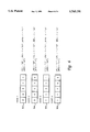
Referring now to FIG. 5, there is depicted an implementation of a four-way LRU field under an illustrative embodiment of the present disclosure. As shown, LRU table 90 comprises five bits. Both bit 90-0 and bit 90-1 are for keeping track of the least recently used set among tag sets 60a-60d, and bits 90-0, 90-1 together contain the LRU set number. Similarly, both bit 90-2 and bit 90-3 are for keeping track of the second least recently used set among tag sets 60a-60d, and bits 90-2, 90-3 together contain the set number of the LRU+1 set number. Bit 90-4 contains a bit for keeping track of the second most recently used set, MRU-1. As an illustrative embodiment, a "1" denotes the higher set number of the two remaining sets as the MRU-1 set, while a "0" denotes the lower set number of the two remaining sets as the MRU-1 set, although it is understood that a reverse assignment is also acceptable. Thus, bit 90-4 will be a "1" if the higher set number of the two remaining sets is the MRU-1. Conversely, bit 90-4 will be a "0" if the lower set number of the two remaining sets is the MRU-1. Finally, the MRU set number is again implicit as it can be determined to be the only remaining set.
With reference now to FIG. 6, there are depicted several examples for illustrating the application of the four-way LRU mechanism according to an illustrative embodiment of the disclosure.
In case 1, as illustrated at reference numeral 92: LRU is "00" means LRU set is set 0; LRU+1 is "01" means LRU+1 set is set 1. Because the MRU-1 bit is "1," this means the higher set number of the remaining two sets is the MRU-1. In this case, the two remaining sets are set 2 and set 3. The higher set number of the two is set 3; hence MRU-1 is set 3, which leaves the remaining set 2 as the MRU set.
In case 2, as illustrated at reference numeral 94: LRU is "00" means LRU set is set 0; LRU+1 is "01" means LRU+1 set is set 1. Because the MRU-1 bit is "0," this means the lower set number of the remaining two sets is the MRU-1. In this case, the remaining two sets are again set 2 and set 3. The lower set number of the two is set 2; hence MRU-1 is set 2, which leaves the remaining set 3 as the MRU set.
In case 3, as illustrated at reference numeral 96: LRU is "11" means LRU set is set 3; LRU+1 is "01" means LRU+1 set is set 1. Because the MRU-1 bit is "1," this means the higher set number of the remaining two sets is the MRU-1. In this case, the remaining two sets are set 0 and set 2. The higher set number of the two is set 2; hence MRU-1 is set 2, which leaves the remaining set 0 as the MRU set.
In case 4, as illustrated at reference numeral 98: LRU is "11" means LRU set is set 3; LRU+1 is "10" means LRU+1 set is set 2. Because the MRU-1 bit is "0," this means the lower set number of the two remaining sets is the MRU-1. In this case, the two remaining sets are set 0 and set 1. The lower set number of the two is set 0; hence MRU-1 is set 0, which leaves the remaining set 1 as the MRU set.
As described, this disclosure provides a method for implementing the four-way LRU mechanism in a high-performance data processing system with only five bits. Although only a four-way cache memory is utilized as an illustration in the present disclosure, it will be understood by those skilled in the art that the principal as illustrated may also be applicable to different cache memories having various numbers of ways and that less than (N-1)log2 N bits, where N=number of ways of the cache memory, are required to implement a LRU mechanism in those cache memories. Take an eight-way cache memory as an example, the first four sets of information, LRU, LRU+1, LRU+2 and LRU+3, may be tracked by twelve bits with three bits for each set. Then, the remaining four sets of information, MRU-3, MRU-2, MRU-1 and MRU, may be tracked by five bits, as illustrated above. Thus, the total bits required to implement a LRU mechanism for an eight-way cache memory, according to the present disclosure, is 17 bits. This is five bits less than the prior art requirement of (8-1)log2 8=21 bits.
In addition, the illustrative embodiment of the present disclosure can be conveniently represented by an empirical formula, as follows: ##EQU1## where x is preferably equal to log2 number of ways of the cache memory! rounding up to a next highest integer.
While the disclosure has been particularly shown and described with reference to an illustrative embodiment, it will be understood by those skilled in the art that various changes in form and detail may be made therein without departing from the spirit and scope of the disclosure.

Claims (8)

What is claimed is:
1. A method for implementing a least recently used cache line replacement scheme in a cache memory having units of information, said method comprising the steps of:
encoding least recently used cache line information for indicating an order of N number of said units by utilizing ##EQU2## bits, wherein x=integer of (log2 N) and N≧4 and using the encoded least recently used cache line information when replacing a cache line in the cache memory.
2. A method of implementing a least recently used cache line replacement scheme in a cache memory, said cache memory having a plurality of cache lines, wherein each cache line includes four congruence sets, said method further comprising the steps of:
associating a least recently used (LRU) field with each of said plurality of cache lines within said cache memory, wherein each said LRU field includes five bits;
storing a set number of a least recently used set among said four congruence sets in two bits of said LRU field associated with a corresponding one of said plurality of cache lines;
storing a set number of a second least recently used set among said four congruence sets in another two bits of said LRU field associated with said corresponding one of said plurality of cache lines;
setting a last bit of said LRU field to a state in response to a determination of a set number of a second most recently used set among said four congruence sets, wherein essential information for tracking said least recently used set is stored in minimal memory.
3. The method for implementing a least recently used cache line replacement scheme in a cache memory according to claim 2, said setting step further includes the step of setting said last bit of said LRU field to a logical "1" in response to a determination of said set number of said second most recently used set is higher than a set number of a most recently used set among said four congruence sets.
4. The method for implementing a least recently used cache line replacement scheme in a cache memory according to claim 2, said setting step further includes the step of setting said last bit of said LRU field to a logical "0" in response to a determination of said set number of said second most recently used set is lower than a set number of a most recently used set among said four congruence sets.
5. A cache memory having a four-way least recently used cache line replacement scheme, said cache memory having a plurality of cache lines, wherein each cache line includes four congruence sets, said cache memory comprising:
means for associating a least recently used (LRU) field with each of said plurality of cache lines within said cache memory, wherein each said LRU field includes five bits;
means for storing a set number of a least recently used set among said four congruence sets in two bits of said LRU field associated with a corresponding one of said plurality of cache lines;
means for storing a set number of a second least recently used set among said four congruence sets in another two bits of said LRU field associated with said corresponding one of said plurality of cache lines;
means for setting a last bit of said LRU field to a state in response to a determination of a set number of a second most recently used set among said four congruence sets, wherein minimal memory is needed to store essential information for tracking said least recently used set.
6. The cache memory having a four-way least recently used cache line replacement scheme according to claim 5, said means for setting further includes means for setting said last bit of said LRU field to a logical "1" in response to a determination of said set number of said second most recently used set is higher than a set number of a most recently used set among said four congruence sets.
7. The cache memory having a four-way least recently used cache line replacement scheme according to claim 5, said means for setting further includes means for setting said last bit of said LRU field to a logical "0" in response to a determination of said set number of said second most recently used set is lower than a set number of a most recently used set among said four congruence sets.
8. The cache memory having a four-way least recently used cache line replacement scheme according to claim 5, said cache memory is within a processor.
US08/641,060 1996-04-29 1996-04-29 Method for implementing a four-way least recently used (LRU) mechanism in high-performance Expired - Fee Related US5765191A (en)

Priority Applications (3)

Application Number Priority Date Filing Date Title
US08/641,060 US5765191A (en) 1996-04-29 1996-04-29 Method for implementing a four-way least recently used (LRU) mechanism in high-performance
KR1019970004597A KR970071286A (en) 1996-04-29 1997-02-15 How to implement a 4-way least recently used mechanism in high performance data processing systems and cache memory
JP10630797A JP3239333B2 (en) 1996-04-29 1997-04-23 Method for implementing LRU mechanism

Applications Claiming Priority (1)

Application Number Priority Date Filing Date Title
US08/641,060 US5765191A (en) 1996-04-29 1996-04-29 Method for implementing a four-way least recently used (LRU) mechanism in high-performance

Publications (1)

Publication Number Publication Date
US5765191A true US5765191A (en) 1998-06-09

Family

ID=24570789

Family Applications (1)

Application Number Title Priority Date Filing Date
US08/641,060 Expired - Fee Related US5765191A (en) 1996-04-29 1996-04-29 Method for implementing a four-way least recently used (LRU) mechanism in high-performance

Country Status (3)

Country Link
US (1) US5765191A (en)
JP (1) JP3239333B2 (en)
KR (1) KR970071286A (en)

Cited By (12)

* Cited by examiner, † Cited by third party
Publication number Priority date Publication date Assignee Title
US6240489B1 (en) * 1999-02-24 2001-05-29 International Business Machines Corporation Method for implementing a pseudo least recent used (LRU) mechanism in a four-way cache memory within a data processing system
US6338120B1 (en) 1999-02-26 2002-01-08 International Business Machines Corporation Apparatus for cache use history encoding and decoding including next lru and next mru and method therefor
US6397298B1 (en) * 1999-07-30 2002-05-28 International Business Machines Corporation Cache memory having a programmable cache replacement scheme
US6446171B1 (en) 2000-03-02 2002-09-03 Mips Technologies, Inc. Method and apparatus for tracking and update of LRU algorithm using vectors
US8533398B2 (en) 2010-11-09 2013-09-10 Microsoft Corporation Combination based LRU caching
US20130339618A1 (en) * 2012-06-15 2013-12-19 International Business Machines Corporation Avoiding aborts due to associativity conflicts in a transactional environment
US20150052315A1 (en) * 2013-08-15 2015-02-19 International Business Machines Corporation Management of transactional memory access requests by a cache memory
US9223687B2 (en) 2012-06-15 2015-12-29 International Business Machines Corporation Determining the logical address of a transaction abort
US9262320B2 (en) 2012-06-15 2016-02-16 International Business Machines Corporation Tracking transactional execution footprint
US9286076B2 (en) 2012-06-15 2016-03-15 International Business Machines Corporation Intra-instructional transaction abort handling
US9298631B2 (en) 2012-06-15 2016-03-29 International Business Machines Corporation Managing transactional and non-transactional store observability
US9298469B2 (en) 2012-06-15 2016-03-29 International Business Machines Corporation Management of multiple nested transactions

Citations (2)

* Cited by examiner, † Cited by third party
Publication number Priority date Publication date Assignee Title
US4607331A (en) * 1983-05-13 1986-08-19 Motorola, Inc. Method and apparatus for implementing an algorithm associated with stored information
US5638531A (en) * 1995-06-07 1997-06-10 International Business Machines Corporation Multiprocessor integrated circuit with video refresh logic employing instruction/data caching and associated timing synchronization

Patent Citations (2)

* Cited by examiner, † Cited by third party
Publication number Priority date Publication date Assignee Title
US4607331A (en) * 1983-05-13 1986-08-19 Motorola, Inc. Method and apparatus for implementing an algorithm associated with stored information
US5638531A (en) * 1995-06-07 1997-06-10 International Business Machines Corporation Multiprocessor integrated circuit with video refresh logic employing instruction/data caching and associated timing synchronization

Cited By (20)

* Cited by examiner, † Cited by third party
Publication number Priority date Publication date Assignee Title
US6240489B1 (en) * 1999-02-24 2001-05-29 International Business Machines Corporation Method for implementing a pseudo least recent used (LRU) mechanism in a four-way cache memory within a data processing system
US6338120B1 (en) 1999-02-26 2002-01-08 International Business Machines Corporation Apparatus for cache use history encoding and decoding including next lru and next mru and method therefor
US6397298B1 (en) * 1999-07-30 2002-05-28 International Business Machines Corporation Cache memory having a programmable cache replacement scheme
US6446171B1 (en) 2000-03-02 2002-09-03 Mips Technologies, Inc. Method and apparatus for tracking and update of LRU algorithm using vectors
US8533398B2 (en) 2010-11-09 2013-09-10 Microsoft Corporation Combination based LRU caching
US9298469B2 (en) 2012-06-15 2016-03-29 International Business Machines Corporation Management of multiple nested transactions
US9262320B2 (en) 2012-06-15 2016-02-16 International Business Machines Corporation Tracking transactional execution footprint
US9483276B2 (en) 2012-06-15 2016-11-01 International Business Machines Corporation Management of shared transactional resources
US9015419B2 (en) * 2012-06-15 2015-04-21 International Business Machines Corporation Avoiding aborts due to associativity conflicts in a transactional environment
US9223687B2 (en) 2012-06-15 2015-12-29 International Business Machines Corporation Determining the logical address of a transaction abort
US9400657B2 (en) 2012-06-15 2016-07-26 International Business Machines Corporation Dynamic management of a transaction retry indication
US9378143B2 (en) 2012-06-15 2016-06-28 International Business Machines Corporation Managing transactional and non-transactional store observability
US9311101B2 (en) 2012-06-15 2016-04-12 International Business Machines Corporation Intra-instructional transaction abort handling
US9286076B2 (en) 2012-06-15 2016-03-15 International Business Machines Corporation Intra-instructional transaction abort handling
US9298631B2 (en) 2012-06-15 2016-03-29 International Business Machines Corporation Managing transactional and non-transactional store observability
US20130339618A1 (en) * 2012-06-15 2013-12-19 International Business Machines Corporation Avoiding aborts due to associativity conflicts in a transactional environment
US20150052315A1 (en) * 2013-08-15 2015-02-19 International Business Machines Corporation Management of transactional memory access requests by a cache memory
US9244725B2 (en) * 2013-08-15 2016-01-26 Globalfoundries Inc. Management of transactional memory access requests by a cache memory
US9244724B2 (en) * 2013-08-15 2016-01-26 Globalfoundries Inc. Management of transactional memory access requests by a cache memory
US20150052311A1 (en) * 2013-08-15 2015-02-19 International Business Machines Corporation Management of transactional memory access requests by a cache memory

Also Published As

Publication number Publication date
KR970071286A (en) 1997-11-07
JP3239333B2 (en) 2001-12-17
JPH1091528A (en) 1998-04-10

Similar Documents

Publication Publication Date Title
US5860107A (en) Processor and method for store gathering through merged store operations
US6425075B1 (en) Branch prediction device with two levels of branch prediction cache
US5564118A (en) Past-history filtered branch prediction
US5519841A (en) Multi instruction register mapper
US5835745A (en) Hardware instruction scheduler for short execution unit latencies
US5619662A (en) Memory reference tagging
Eickemeyer et al. A load-instruction unit for pipelined processors
US5918245A (en) Microprocessor having a cache memory system using multi-level cache set prediction
US5778434A (en) System and method for processing multiple requests and out of order returns
US7958317B2 (en) Cache directed sequential prefetch
US20090198900A1 (en) Microprocessor Having a Power-Saving Instruction Cache Way Predictor and Instruction Replacement Scheme
EP0927394B1 (en) A cache line branch prediction scheme that shares among sets of a set associative cache
US5765199A (en) Data processor with alocate bit and method of operation
US5765191A (en) Method for implementing a four-way least recently used (LRU) mechanism in high-performance
US5737749A (en) Method and system for dynamically sharing cache capacity in a microprocessor
US5682495A (en) Fully associative address translation buffer having separate segment and page invalidation
US20080046652A1 (en) Processor having a micro tag array that reduces data cache access power, and applicatons thereof
US6240489B1 (en) Method for implementing a pseudo least recent used (LRU) mechanism in a four-way cache memory within a data processing system
US5875325A (en) Processor having reduced branch history table size through global branch history compression and method of branch prediction utilizing compressed global branch history
US5832249A (en) High performance superscalar alignment unit
US5581719A (en) Multiple block line prediction
US5802340A (en) Method and system of executing speculative store instructions in a parallel processing computer system
US5678016A (en) Processor and method for managing execution of an instruction which determine subsequent to dispatch if an instruction is subject to serialization
US5787479A (en) Method and system for preventing information corruption in a cache memory caused by an occurrence of a bus error during a linefill operation
US5715420A (en) Method and system for efficient memory management in a data processing system utilizing a dual mode translation lookaside buffer

Legal Events

Date Code Title Description
AS Assignment

Owner name: INTERNATIONAL BUSINESS MACHINES CORPORATION, NEW Y

Free format text: ASSIGNMENT OF ASSIGNORS INTEREST;ASSIGNORS:LOPER, ALBERT JOHN;MALLICK, SOUMMYA;PATEL, RAJESH BHIKHUBHAI;AND OTHERS;REEL/FRAME:008086/0151;SIGNING DATES FROM 19960412 TO 19960419

FEPP Fee payment procedure

Free format text: PAYOR NUMBER ASSIGNED (ORIGINAL EVENT CODE: ASPN); ENTITY STATUS OF PATENT OWNER: LARGE ENTITY

CC Certificate of correction
REMI Maintenance fee reminder mailed
LAPS Lapse for failure to pay maintenance fees

Free format text: PATENT EXPIRED FOR FAILURE TO PAY MAINTENANCE FEES (ORIGINAL EVENT CODE: EXP.); ENTITY STATUS OF PATENT OWNER: LARGE ENTITY

STCH Information on status: patent discontinuation

Free format text: PATENT EXPIRED DUE TO NONPAYMENT OF MAINTENANCE FEES UNDER 37 CFR 1.362

FP Lapsed due to failure to pay maintenance fee

Effective date: 20020609