US5754454A - Method for determining functional equivalence between design models - Google Patents
Method for determining functional equivalence between design models Download PDFInfo
- Publication number
- US5754454A US5754454A US08/808,759 US80875997A US5754454A US 5754454 A US5754454 A US 5754454A US 80875997 A US80875997 A US 80875997A US 5754454 A US5754454 A US 5754454A
- Authority
- US
- United States
- Prior art keywords
- cutpoint
- pair
- pair candidate
- bdd
- candidate
- Prior art date
- Legal status (The legal status is an assumption and is not a legal conclusion. Google has not performed a legal analysis and makes no representation as to the accuracy of the status listed.)
- Expired - Lifetime
Links
Images


Classifications
-
- G—PHYSICS
- G06—COMPUTING; CALCULATING OR COUNTING
- G06F—ELECTRIC DIGITAL DATA PROCESSING
- G06F30/00—Computer-aided design [CAD]
- G06F30/30—Circuit design
- G06F30/32—Circuit design at the digital level
- G06F30/33—Design verification, e.g. functional simulation or model checking
- G06F30/3323—Design verification, e.g. functional simulation or model checking using formal methods, e.g. equivalence checking or property checking
Definitions
- the present invention relates generally to semiconductor device verification, and specifically to verifying identical functionality between separate semiconductor design models.
- Formal design verification is the use of mathematical techniques to attempt to achieve 100% of accuracy and coverage, and has recently received attention as an alternative to simulation for some applications. But the circuit size to which formal verification approaches can be applied is often limited.
- One problem with formal design verification is logic checking. During the VLSI chip design process, logic checking is used to verify blocks of combinational logic in different design models that are believed to be identical. However, the use of formal approaches for logic checking has a worst case complexity that is NP-hard, making verification inherently difficult for large circuits.
- BDDs Functional methods using BDD are based upon a graphical representation for Boolean functions.
- BDDs have several desirable characteristics including: (1) Most commonly encountered functions can be represented in a reasonable size of space. (2) It is a canonical form, in that every Boolean function has its own unique representation. (3) Boolean operations of two functions can be efficiently performed. Thus, BDDs have been used for many CAD applications where Boolean functions are used.
- FIG. 1 illustrates, in block and logic diagram form, a logic representation of two design files
- FIG. 2 illustrates, in block diagram form, a portion of FIG. 1 known as a cone of logic
- FIG. 3 illustrates, in flow diagram form, a method in accordance with the present invention
- FIG. 4 illustrates, in block and logic diagram form, a portion of the two models of FIG. 1;
- FIG. 5 illustrates, in logic and flow form, a binary decision diagram (BDD) and truth table for a logic portion of FIG. 1;
- BDD binary decision diagram
- FIG. 6 illustrates, in logic and flow form, a binary decision diagram (BDD) and truth table for a logic portion of FIG. 1;
- BDD binary decision diagram
- FIG. 7 illustrates, in logic and flow form, a binary decision diagram (BDD) and truth table for a logic portion of FIG. 1;
- BDD binary decision diagram
- FIG. 8 illustrates, in logic and flow form, a binary decision diagram (BDD) and truth table for a logic portion of FIG. 1;
- FIG. 9 illustrates, in flow form, the results of substituting one BDD into a second BDD.
- FIG. 10 illustrates, a block diagram for computer system in accordance with present system.
- FIG. 11 illustrates, a flow diagram in accordance with present invention.
- the present invention determines whether two design files have identical functionality by attempting to create a binary decision diagram (BDD) for corresponding verification output pairs.
- BDD binary decision diagram
- An automatic test program generator (ATPG) is used to determine whether or not the cutpoint pair candidates are invalid cutpoints. The invalid cutpoints are removed from the set of cutpoint pair candidates.
- a cutpoint pair candidate having known support is selected.
- Known support, or known input is defined to mean all inputs to a cutpoint pair are a combination of verification inputs, primary inputs, and cutpoint variables.
- An exclusive-or of the outputs of the selected candidate is formed.
- a BDD for the resulting XOR function is attempted.
- the selected candidate is valid indicating equivalence or inversion. If the BDD is neither the zero function nor the one function, the cutpoint pair is invalid providing all of its inputs are verification inputs. If one or more of the inputs are cutpoint variable inputs, the function for a cutpoint variable input is substituted, and the flow continues to build a new BDD for the evaluation XOR having the substituted function.
- FIG. 1 illustrates a design model 100 being compared to a design model 150.
- Model 100 comprises a logic diagram which could have been derived from a register transfer logic (RTL) model or from a gate level model.
- RTL register transfer logic
- circuit portions 110, 115, 120, 125, and 130 are refered to as subblocks of the model.
- Each of circuit portions 110, 115, 120, 125, and 130 contain a latch 111, 116, 121, 126, 131, and a cone of logic 112, 117, 122, 127, and 132 respectively.
- the input to a latch or a primary output of the model is referred to as a verification output.
- While the output of a latch or a primary input is referred to as a verification input.
- the value of a verification output is controlled by its associated cone of logic.
- the associated cone of logic includes all logic coupled to the verification output without an intervening latches.
- the cone of logic coupled to verification node 118 includes cone 116, cone 111, and cone 121.
- the associated cone of logic can receive verification inputs, and cutpoint variables as discussed in more detail later.
- An input labeled INA is connected to an input of the circuit portion 110.
- the verification output of Circuit portion 110 namely net 113, is connected to an input of Circuit portion 116.
- the verification output 118 of Circuit portion 116 is connected to output node labeled OUTA.
- An input labeled INB is connected to an input of Circuit portion 120.
- the verification output 123 of Circuit portion 120 is connected to an input of Circuit portion 125, and Circuit portion 115.
- the verification output 128 of Circuit portion 125 is connected to an input of Circuit portion 130, and to an output node labeled OUTC.
- the verification output 133 of Circuit portion 130 is connected to and output labeled OUTB.
- the inputs INA, INB, and the outputs OUTA, OUTB, and OUTC may be individual input signals or represent multiple inputs.
- the inputs A, B, C, and D of FIG. 2 are INA of FIG. 1.
- the design 150 has similar connectivity as design 100 with corresponding locations incremented by 50 exists for design 150.
- FIG. 2 illustrates a more detailed view of the corresponding cones of logic 111 and 161.
- the cone of logic 111 is part of the Circuit portion 110 of design 100
- the cone of logic 161 is part of the Circuit portion 160 of design 150.
- Cone of logic 111 comprises smaller cones of logic 210, 215, 220, 225, and 230.
- the point of each cone of logic represents a cutpoint candidate location in our example.
- Cone of logic 161 comprises smaller cones of logic 260, 265, 270, 275, and 280.
- the point of each cone of logic represents a cutpoint candidate location in our example.
- Both cones of logic 111, 161 receive inputs labeled A, B, C, and D.
- the input A is connected to cones of logic 220 and 270.
- the input B is connected to the cones of logic 220, 225, 270, and 275.
- the input C is connected to cones of logic 210 and 260.
- the input D is connected to cones of logic 210, 220, 260, and 270.
- the output of cone of logic 210 forms a cutpoint candidate in our example labeled VW and is connected to cone of logic 215.
- the output of cone of logic 220 forms cutpoint candidate X1 221 and is connected to cone of logic 215 and 225.
- the output of cone of logic 215 forms an unlabeled cutpoint candidate and is connected to cone of logic 230.
- the output of cone of logic 225 forms cutpoint Y1 226, and is connected to cone of logic 230.
- the output of cone of logic 230 is connected to the output node 113.
- the output of cone of logic 260 forms a cutpoint labeled VW and is connected to cone of logic 265.
- the output of cone of logic 270 forms cutpoint X2 271 and is connected to cone of logic 265 and 275.
- the output of cone of logic 265 forms an unlabeled cutpoint and is connected to cone of logic 280.
- the output of cone of logic 275 forms cutpoint Y2 276, and is connected to cone of logic 280.
- the output of cone of logic 280 is connected to the output node 163.
- the output node 118 and 168 form a corresponding output pair.
- the method 300 of FIG. 3 comprises rectangular shaped operations steps 301 through 313, diamond shaped evaluation steps 320 through 324, and an oval termination step 330.
- FIG. 4 illustrates an expanded view of Circuit portions 110 and 160 of FIG. 1.
- cone of logic 220 comprises a two input or- gate 211.
- Cone of logic 270 comprises a two input or gate 261.
- Cone of logic 225 comprises a two input exclusive-or gate 261.
- Cone of logic 275 comprises an inverter 224 connected to an and-gate 272.
- a first model 100 is being compared to a second model 150.
- the models 100 and 150 represent related designs that should be functionally identical.
- the models 100 and 150 are shown to contain circuit portions 110, 115, 120, 125, 130, 160, 165, 170, 175, and 180. Different functional models may be used for model 100 and model 150 with the present invention. Circuit portions are illustrated in FIG. 1 for example purposes only.
- each Circuit portion there is a cone of logic which represents a combinational logic portion of the Circuit portion.
- the combinational logic is prohibited from providing feedback within the cone of logic. This implies that there is no loop of logic in the circuit that in unbroken my a latch.
- FIG. 2 it is illustrated that a cone of logic 111 and 161 from FIG. 1 may be further divided into smaller cones of logic.
- FIG. 3 which illustrates a detailed portion of FIG. 2, will be discussed further below.
- Method 300 of FIG. 3 illustrates one embodiment of the present invention.
- latches between the first and a second design model 100 and 150 are paired.
- latch 112 of design 100 is paired to latch 162 of design 150.
- Latch 117 is paired to latch 167.
- Latch 122 is paired to latch 172.
- Latch 127 is paired to latch 177.
- Latch 1132 is paired to latch 182.
- These pairings identify nodes forming verification output pairs (Nodes 113 and 163, 118 and 168, 123 and 173, 128 and 178, 132 and 182 are corresponding verification output pairs).
- the cones of logic illustrated in FIG. 1 as part of the circuit portions drive the verification output pairs.
- the pairing of the latches in step 301 can be done either automatically or by user input.
- One method of automatically pairing latches is described in U.S. Pat. No. 5,638,381 (08/505,431) by Cho. (Note, the Issue Fee has been submitted, however the application has not yet issued.)
- the registers are paired, their corresponding cones of logic can be identified.
- identity between the designs 100 and 150 can be determined.
- an attempt is made to create a BDD for those corresponding verification output pairs meeting a predefined threshold.
- a threshold is based upon the number of levels of logic driving each output pair. As previously discussed, as Boolean function representations become larger, it requires exponentially more resources in terms of memory and/or execution time. A threshold of approximately ten levels of logic or less has been determined to be an efficient threshold. A threshold of ten limits the BDD creation of step 302 to only those corresponding outputs whose function is derived by ten levels of logic or less. For example, in FIG. 1, cone of logic 111, could have a threshold of logic less than ten while cone of logic 12 does not.
- step 320 the pairs having BDDs generated successfully are acted upon by step 312 which then determine whether they match and mark them as verified.
- the flow continues to step 323 from step 312 and step 320 where it is determined whether there are any corresponding verification output pairs that have not been resolved, where resolved indicates that the pair has been shown definitely to be equivalent or not be equivalent.
- the corresponding verification output pairs not meeting the threshold of step 302, and those not having a BDD generated successfully in step 320, are passed into step 323 from step 320 and step 312.
- cutpoint pair candidates are identified using a random simulation.
- the cutpoint pair candidates exist within the cones of logic associated with each of the corresponding verification output pairs. Cutpoint pair candidates are nodes believed to be identical in the two designs. Referring to FIG. 2, the cutpoint pairs for cones of logic 111 and 161 are VW and VW, X1 and X2, and Y1 and Y2. Note that the nodes labeled VW in FIG. 2 represent a cutpoint candidate pair that has been determined valid, as opposed to the variables X1 and X2 which comprise a cutpoint candidate pair which has not yet been validated.
- One method of identifying cutpoint pair candidates is to supply a parallel random pattern simulation to cones 111 and 161. Note, this may be done to the entire design 100 and 150 at one time. Based on the random simulation, the vertices with identical signatures are grouped together. The resulting identity groups are called simulation signature groups. We apply a large number of patterns so that simulating more patterns would not be of much help to distinguish additional non-related vertices. Note that random simulation is not strong enough to distinguish all non-related vertex pairs. Note also that the term identical signatures also anticipates signatures that are inversions of each other. For purposes of example, the cutpoint pairs X1 and X2 and Y1 and Y2 of FIG. 2 are illustrated in more detail in FIG. 4. Where design module information is available, it is beneficial to choose cutpoint candidates for further analysis which are on boundaries of sub-modules. Following step 303, the method 300 continues at step 304.
- a structure based verification tool such as an automatic test program generator (ATPG) is used to screen out invalid cutpoint pairs. This is accomplished by submitting each cutpoint pair candidate to an ATPG tool which attempts to force different output values on the cutpoint pair candidate from common set of common input values.
- ATPG programs have not been used to quickly eliminate bad cutpoint pair candidates.
- One embodiment of the present invention limits the resources that the ATPG program can dedicate to determining validity of any given candidate. The limitation will generally be based upon time or memory allocation. This is especially beneficial over the prior art, in that for large circuits ATPG programs can take very long periods of time. Therefore the present invention is advantageous over the prior art in that in limits the amount of time spent trying to resolve specific portions of logic with a specific method.
- a cutpoint pair candidate is identified (the identified candidate) that has known support.
- known support refers to the fact that all inputs to the identified candidate (or cone of logic) are verification inputs or cutpoint variables. Generally, the candidate selected first will be the candidate closest to the verification inputs.
- an exclusive-or (XOR) model of the selected candidate is formed.
- the XOR model is formed by connecting an exclusive-or gate between the nodes forming the cutpoint pair candidate. If there is identity between the cutpoint pair, the XOR model will always be zero, indicating an exact match, or one, indicating an inverted match.
- a BDD is generated for the XOR model.
- the BDD generation of step 308 can be terminated if it takes up to many resources as discussed previously with reference to ATPG generation. When this occurs the status of the attempted generation will be stored as part of the determination of step 324, and flow will proceed back to step 306. If BDD generation does succeed at step 308, the method 300 continues to step 321.
- a determination is made whether or not the BDD indicates an identity match. It should be noted that identity is indicated when the BDD is equal to zero or one, indicating identical node results, or opposite node results respectively. Where identity is not determined, a subsequent determination is made at step 322 as to whether or the variable inputs are cutpoint variables.
- step 311 the candidate is removed from the set of candidates because it is not a valid cutpoint. If there remains a cutpoint variable, flow proceeds to step 309, where the functional model for a cutpoint variable is substituted into the XOR model.
- step 306 flow proceeds back to step 306 where another cutpoint pair candidate is identified.
- the flow discussed above will continue, and will converge until the corresponding output pairs 118 and 168 are compared. At this point identity for the corresponding verification output is established and flow continues at step 323 to process another corresponding verification output. Once all corresponding verification outputs are processed, design integrity is established.
- FIGS. 4 through 9 provide an example of the method 300.
- FIG. 4 illustrates cutpoint pairs X1 and X2 and Y1 and Y2, and their associated cones of logic. In reality, cones of logic of one and two gates would generally be avoided but will be used herein for the purpose of example.
- the fact that cutpoint pairs have been identified implies that we have completed step 303 of the method 300. Proceeding to step 304, an ATPG program is run on the pairs to determine whether any of the cutpoints can be eliminated. By way of example, it is assumed no elimination results.
- step 305 both pairs are included in the set of cutpoint candidates to be analyzed.
- the pair X1 and X2 would be identified as having known support, since its inputs are either primary inputs or verification inputs from latches as illustrated in FIG. 1.
- step 307 an evaluation XOR model (not shown) is formed.
- the BDD for this model would be built at step 308, and at step 321 the BDD would be zero indicating identity. (This result is intuitive in that both cones 220 and 270 consist of a single or-gate.)
- the nodes X1 and X2 would be replace with the variable (VX) indicating that it is now a valid cutpoint.
- VX variable
- the function of X, for inputs A and B is stored.
- step 306 the candidate pair Y1 and Y2 is analyzed.
- step 307 the XOR model is created, as indicated in FIG. 8, the XOR model is the function of cone 225 and cone 275 XORed together.
- step 308 a BDD is built for the XOR model. For illustration purposes, the BDDs for cone of logic 225 and for cone of logic 275 are illustrated separately.
- the cone of logic 225 is illustrated along with its truth table 502 and BDD 504. Note that the inputs to the cutpoint pair represented by cones 225 cones 225 and 275 are the cutpoint variable X and the primary input B, and its output is Y1. Therefor the truth table 502 and BDD 504 use these nodes to describe the function of the gate 212. In FIG. 7, the cone 275 is illustrated along with its truth table 602 and BDD 604.
- FIG. 8 illustrates the XOR model connected to the nodes Y1 and Y2.
- the BDD 804 it can be seen that the BDD has both a zero value and a one value. Therefore, at step 321, no identity will be determined and flow will proceed to step 322.
- a determination will be made that one of the variables (X) is a cutpoint variable, and flow will proceed to step 309.
- the function for X in FIG. 5 is substituted into the equation for the XOR model of FIG. 8. This is illustrated in FIG. 9, where the BDD 504 for X is substituted for the node X in the BDD 704 for the XOR model of FIG. 8.
- step 321 detects an valid cutpoint and flow will proceed to step 310 where nodes Y1 and Y2 will be identified as a match, and a common variable VY will replace Y1 and Y2, and the function of VY will be stored.
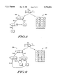
- a typical hardware configuration of a workstation which may be implemented to accomplish the methodologies disclosed herein, is illustrated and includes a central processing unit (CPU) 10, such as a conventional microprocessor, and a number of other units interconnected via system bus 12.
- CPU central processing unit
- the workstation shown in FIG. 1 includes random access memory (RAM) 14, read only memory (ROM) 16, and input/output (I/O) adapter 18 for connecting peripheral devices, such as disk units 20 and tape units 40, to bus 12.
- RAM random access memory
- ROM read only memory
- I/O input/output
- a user interface adapter 22 is used to connect a keyboard device 24 and a mouse 26 to the system bus 12.
- Other user interface devices such as a touch screen device (not shown) may also be coupled to the system bus 12 through the user interface adapter 22.
- a communication adapter 34 is also shown for connecting the workstation to a data processing network 17. Further, a display adapter 36 connects the system bus 12 to a display device 38.
- the method of the present invention may be implemented and stored in one or more of the disk units 20, tape drives 40, ROM 16 and/or RAM 14, or even made available to system 13 via a network connection through communications adapter 34 and thereafter processed by CPU 10. Since the apparatus implementing the present invention is, for the most part, composed of electronic components and circuits known to those skilled in the art, circuit details will not be explained in any greater extent than that considered necessary as illustrated above, for the understanding and appreciation of the underlying concepts of the present invention and in order not to obfuscate or distract from the teachings of the present invention.
- FIG. 11 is a block diagram that illustrates integrated circuit fabrication utilizing the optimized circuit resulting from the method 300 of FIG. 3.
- the optimization tool 52 utilizes circuit models 50 to generate an optimized circuit layout 54.
- a physical design file 58 is generated 56 from the optimized circuit layout 54.
- the circuit models 50, optimized circuit layout 54, and physical design 58 are typically stored as data files on computer readable media such as disk units 20.
- the physical design file 58 includes integrated circuit dimensions, element dimensions, and element locations within the integrated circuit.
- the physical design file 58 locates elements and connections within a two-dimensional substrate area of an integrated circuit die.
- the physical design file 58 includes physical structure for performing the functions of an integrated circuit design from which the physical design file 58 was derived.
- the physical design 58 is converted 60 into a set of lithographic masks 62 corresponding to the layers in the physical design file 58.
- the lithographic masks 62 are used to fabricate 64 integrated circuits 66.
- CAD computer aided design
- the present invention could be used within step 52 to verify optimizations to a circuit layout or design model.
- These files are then used to form lithographic masks which are then used to form a plurality of integrated circuits on a plurality of wafers using an integrated circuit fabrication facility.
- the design phase is taught in "Principles of CMOS VLSI Design: A Systems Perspective", by N. H. E. Weste and K. Eshragian in the VLSI Series by Addison-Wesley, 1985.
Landscapes
- Engineering & Computer Science (AREA)
- Computer Hardware Design (AREA)
- Physics & Mathematics (AREA)
- Theoretical Computer Science (AREA)
- Evolutionary Computation (AREA)
- Geometry (AREA)
- General Engineering & Computer Science (AREA)
- General Physics & Mathematics (AREA)
- Design And Manufacture Of Integrated Circuits (AREA)
Abstract
Description
Claims (27)
Priority Applications (1)
| Application Number | Priority Date | Filing Date | Title |
|---|---|---|---|
| US08/808,759 US5754454A (en) | 1997-03-03 | 1997-03-03 | Method for determining functional equivalence between design models |
Applications Claiming Priority (1)
| Application Number | Priority Date | Filing Date | Title |
|---|---|---|---|
| US08/808,759 US5754454A (en) | 1997-03-03 | 1997-03-03 | Method for determining functional equivalence between design models |
Publications (1)
| Publication Number | Publication Date |
|---|---|
| US5754454A true US5754454A (en) | 1998-05-19 |
Family
ID=25199645
Family Applications (1)
| Application Number | Title | Priority Date | Filing Date |
|---|---|---|---|
| US08/808,759 Expired - Lifetime US5754454A (en) | 1997-03-03 | 1997-03-03 | Method for determining functional equivalence between design models |
Country Status (1)
| Country | Link |
|---|---|
| US (1) | US5754454A (en) |
Cited By (43)
| Publication number | Priority date | Publication date | Assignee | Title |
|---|---|---|---|---|
| US5949691A (en) * | 1996-08-15 | 1999-09-07 | Nec Corporation | Logic circuit verification device to verify the logic circuit equivalence and a method therefor |
| US5974242A (en) * | 1997-09-25 | 1999-10-26 | The United States Of America As Represented By The Secretary Of The Army | Methods and computer programs for minimizing logic circuit design using identity cells |
| US6026222A (en) * | 1997-12-23 | 2000-02-15 | Nec Usa, Inc. | System for combinational equivalence checking |
| US6035107A (en) * | 1997-08-28 | 2000-03-07 | International Bunsiness Machines Corporation | Method for performing functional comparison of combinational circuits |
| WO2000026824A1 (en) * | 1998-11-03 | 2000-05-11 | Siemens Aktiengesellschaft | Method and arrangement for comparing a first characteristic with given characteristics of a technical system |
| WO2000026825A1 (en) * | 1998-11-03 | 2000-05-11 | Siemens Aktiengesellschaft | Method and device for comparing technical systems with each other |
| US6138266A (en) * | 1997-06-16 | 2000-10-24 | Tharas Systems Inc. | Functional verification of integrated circuit designs |
| US6148436A (en) * | 1998-03-31 | 2000-11-14 | Synopsys, Inc. | System and method for automatic generation of gate-level descriptions from table-based descriptions for electronic design automation |
| US6247165B1 (en) * | 1998-03-31 | 2001-06-12 | Synopsys, Inc. | System and process of extracting gate-level descriptions from simulation tables for formal verification |
| US6301687B1 (en) * | 1997-05-16 | 2001-10-09 | Fujitsu Limited | Method for verification of combinational circuits using a filtering oriented approach |
| US6308299B1 (en) * | 1998-07-17 | 2001-10-23 | Cadence Design Systems, Inc. | Method and system for combinational verification having tight integration of verification techniques |
| US6321173B1 (en) | 1998-12-10 | 2001-11-20 | Hewlett-Packard Company | System and method for efficient verification of functional equivalence between design models |
| US6339837B1 (en) | 1998-02-25 | 2002-01-15 | Zhe Li | Hybrid method for design verification |
| US6367064B1 (en) * | 1998-05-22 | 2002-04-02 | Micron Technology, Inc. | Verification of sensitivity list integrity in a hardware description language file |
| US6378116B1 (en) * | 1999-05-28 | 2002-04-23 | Cadence Design Systems, Inc. | Using budgeted required time during technology mapping |
| US6405345B1 (en) | 1999-05-28 | 2002-06-11 | Cadence Design Systems, Inc. | Updating placement during technology mapping |
| US20020144215A1 (en) * | 2001-03-09 | 2002-10-03 | Hoskote Yatin V. | System and method for automatically mapping state elements for equivalence verification |
| US6473884B1 (en) | 2000-03-14 | 2002-10-29 | International Business Machines Corporation | Method and system for equivalence-checking combinatorial circuits using interative binary-decision-diagram sweeping and structural satisfiability analysis |
| US6490710B1 (en) * | 2000-04-06 | 2002-12-03 | Mitsubishi Denki Kabushiki Kaisha | Logic verification method and apparatus for logic verification |
| US6536016B1 (en) * | 2000-07-27 | 2003-03-18 | Lsi Logic Corporation | Method and apparatus for locating constants in combinational circuits |
| US6560755B1 (en) | 2000-08-24 | 2003-05-06 | Cadence Design Systems, Inc. | Apparatus and methods for modeling and simulating the effect of mismatch in design flows of integrated circuits |
| US6564358B2 (en) * | 2000-12-11 | 2003-05-13 | Intel Corporation | Method and system for formal verification of a circuit model using binary decision diagrams |
| US6591400B1 (en) | 2000-09-29 | 2003-07-08 | Intel Corporation | Symbolic variable reduction |
| KR100395160B1 (en) * | 2001-11-20 | 2003-08-19 | 한국전자통신연구원 | Method for synthesizing two-level logic |
| US6611947B1 (en) * | 2000-08-23 | 2003-08-26 | Jasper Design Automation, Inc. | Method for determining the functional equivalence between two circuit models in a distributed computing environment |
| US6643827B1 (en) | 2000-09-30 | 2003-11-04 | Intel Corporation | Symbolic model checking with dynamic model pruning |
| US6662323B1 (en) * | 1999-07-07 | 2003-12-09 | Nec Corporation | Fast error diagnosis for combinational verification |
| US6725431B1 (en) | 2000-06-30 | 2004-04-20 | Intel Corporation | Lazy symbolic model checking |
| US20040093574A1 (en) * | 2002-11-07 | 2004-05-13 | John Moondanos | Method and apparatus for cut-point frontier selection and for counter-example generation in formal equivalence verification |
| US20040103378A1 (en) * | 2002-11-13 | 2004-05-27 | Fujitsu Limited | System and method for building a binary decision diagram associated with a target circuit |
| US20040130313A1 (en) * | 2002-11-08 | 2004-07-08 | Dong Xiang | Method for reducing pin overhead in non-scan design for testability |
| US20040177332A1 (en) * | 2003-03-07 | 2004-09-09 | Manish Pandey | Method and system for logic equivalence checking |
| US20050071347A1 (en) * | 2003-09-30 | 2005-03-31 | International Business Machines Corporation | System and method for conversion between graph-based representations and structural text-based representations of business processes |
| US6931611B2 (en) | 2001-12-19 | 2005-08-16 | Freescale Semiconductor, Inc. | Design verification system for avoiding false failures and method therefor |
| US20050192789A1 (en) * | 2000-06-30 | 2005-09-01 | Jin Yang | Methods for formal verification on a symbolic lattice domain |
| US6993730B1 (en) | 2001-01-10 | 2006-01-31 | Tempus Fugit, Inc. | Method for rapidly determining the functional equivalence between two circuit models |
| US7031896B1 (en) | 2000-06-30 | 2006-04-18 | Intel Corporation | Methods for performing generalized trajectory evaluation |
| US20060101359A1 (en) * | 2002-08-29 | 2006-05-11 | Stefan Horeth | Method and device for verifying digital circuits |
| US7216318B1 (en) | 2003-04-29 | 2007-05-08 | Cadence Design Systems, Inc. | Method and system for false path analysis |
| US20090064071A1 (en) * | 2003-04-29 | 2009-03-05 | Cadence Design Systems, Inc. | Method and system for global coverage analysis |
| US10503852B2 (en) * | 2017-01-19 | 2019-12-10 | Imagination Technologies Limited | Formal verification of integrated circuit hardware designs to implement integer division |
| US11023357B1 (en) * | 2019-09-26 | 2021-06-01 | Cadence Design Systems, Inc. | Method and system for sequential equivalence checking |
| US11076219B2 (en) * | 2019-04-12 | 2021-07-27 | Bose Corporation | Automated control of noise reduction or noise masking |
Citations (3)
| Publication number | Priority date | Publication date | Assignee | Title |
|---|---|---|---|---|
| US5331568A (en) * | 1991-06-18 | 1994-07-19 | Microelectronics & Computer Technology Corporation | Apparatus and method for determining sequential hardware equivalence |
| US5572535A (en) * | 1994-07-05 | 1996-11-05 | Motorola Inc. | Method and data processing system for verifying the correct operation of a tri-state multiplexer in a circuit design |
| US5649165A (en) * | 1995-01-31 | 1997-07-15 | Fujitsu Limited | Topology-based computer-aided design system for digital circuits and method thereof |
-
1997
- 1997-03-03 US US08/808,759 patent/US5754454A/en not_active Expired - Lifetime
Patent Citations (3)
| Publication number | Priority date | Publication date | Assignee | Title |
|---|---|---|---|---|
| US5331568A (en) * | 1991-06-18 | 1994-07-19 | Microelectronics & Computer Technology Corporation | Apparatus and method for determining sequential hardware equivalence |
| US5572535A (en) * | 1994-07-05 | 1996-11-05 | Motorola Inc. | Method and data processing system for verifying the correct operation of a tri-state multiplexer in a circuit design |
| US5649165A (en) * | 1995-01-31 | 1997-07-15 | Fujitsu Limited | Topology-based computer-aided design system for digital circuits and method thereof |
Non-Patent Citations (6)
| Title |
|---|
| C. Leonard Berman, et al., "Functional Comparison of Logic Designs for VLSI Circuits", 1989 IEEE, CH2805-0/89/0000/0456, pp. 456-459. |
| C. Leonard Berman, et al., Functional Comparison of Logic Designs for VLSI Circuits , 1989 IEEE, CH2805 0/89/0000/0456, pp. 456 459. * |
| Masahiro Fujita, et al., "Evaluation and Improvements of Boolean Comparison Method Based on Binary Decision Diagrams", 1988 IEEE, CH2657-5/88, 4 pgs. |
| Masahiro Fujita, et al., Evaluation and Improvements of Boolean Comparison Method Based on Binary Decision Diagrams , 1988 IEEE, CH2657 5/88, 4 pgs. * |
| Yusuke Matsunaga, "An Efficient Equivalence Checker for Combinational Circuits", 33rd Design Automation Conf., ACM 0-8979-1-779-0/96/0006, pp. 629-634. |
| Yusuke Matsunaga, An Efficient Equivalence Checker for Combinational Circuits , 33rd Design Automation Conf., ACM 0 8979 1 779 0/96/0006, pp. 629 634. * |
Cited By (63)
| Publication number | Priority date | Publication date | Assignee | Title |
|---|---|---|---|---|
| US5949691A (en) * | 1996-08-15 | 1999-09-07 | Nec Corporation | Logic circuit verification device to verify the logic circuit equivalence and a method therefor |
| US6301687B1 (en) * | 1997-05-16 | 2001-10-09 | Fujitsu Limited | Method for verification of combinational circuits using a filtering oriented approach |
| US6138266A (en) * | 1997-06-16 | 2000-10-24 | Tharas Systems Inc. | Functional verification of integrated circuit designs |
| US6035107A (en) * | 1997-08-28 | 2000-03-07 | International Bunsiness Machines Corporation | Method for performing functional comparison of combinational circuits |
| US5974242A (en) * | 1997-09-25 | 1999-10-26 | The United States Of America As Represented By The Secretary Of The Army | Methods and computer programs for minimizing logic circuit design using identity cells |
| US6026222A (en) * | 1997-12-23 | 2000-02-15 | Nec Usa, Inc. | System for combinational equivalence checking |
| US6339837B1 (en) | 1998-02-25 | 2002-01-15 | Zhe Li | Hybrid method for design verification |
| US6148436A (en) * | 1998-03-31 | 2000-11-14 | Synopsys, Inc. | System and method for automatic generation of gate-level descriptions from table-based descriptions for electronic design automation |
| US6247165B1 (en) * | 1998-03-31 | 2001-06-12 | Synopsys, Inc. | System and process of extracting gate-level descriptions from simulation tables for formal verification |
| US6367064B1 (en) * | 1998-05-22 | 2002-04-02 | Micron Technology, Inc. | Verification of sensitivity list integrity in a hardware description language file |
| US6308299B1 (en) * | 1998-07-17 | 2001-10-23 | Cadence Design Systems, Inc. | Method and system for combinational verification having tight integration of verification techniques |
| WO2000026825A1 (en) * | 1998-11-03 | 2000-05-11 | Siemens Aktiengesellschaft | Method and device for comparing technical systems with each other |
| US6581026B2 (en) | 1998-11-03 | 2003-06-17 | Infineon Technologies Ag | Method and configuration for comparing a first characteristic with predetermined characteristics of a technical system |
| WO2000026824A1 (en) * | 1998-11-03 | 2000-05-11 | Siemens Aktiengesellschaft | Method and arrangement for comparing a first characteristic with given characteristics of a technical system |
| US6321173B1 (en) | 1998-12-10 | 2001-11-20 | Hewlett-Packard Company | System and method for efficient verification of functional equivalence between design models |
| US6378116B1 (en) * | 1999-05-28 | 2002-04-23 | Cadence Design Systems, Inc. | Using budgeted required time during technology mapping |
| US6405345B1 (en) | 1999-05-28 | 2002-06-11 | Cadence Design Systems, Inc. | Updating placement during technology mapping |
| US20040030974A1 (en) * | 1999-07-07 | 2004-02-12 | Nec Corporation | Fast error diagnosis for combinational verification |
| US6662323B1 (en) * | 1999-07-07 | 2003-12-09 | Nec Corporation | Fast error diagnosis for combinational verification |
| US6473884B1 (en) | 2000-03-14 | 2002-10-29 | International Business Machines Corporation | Method and system for equivalence-checking combinatorial circuits using interative binary-decision-diagram sweeping and structural satisfiability analysis |
| US6490710B1 (en) * | 2000-04-06 | 2002-12-03 | Mitsubishi Denki Kabushiki Kaisha | Logic verification method and apparatus for logic verification |
| US6725431B1 (en) | 2000-06-30 | 2004-04-20 | Intel Corporation | Lazy symbolic model checking |
| US20070050181A1 (en) * | 2000-06-30 | 2007-03-01 | Jin Yang | Antecedent strengthening to perform generalized trajectory evaluation |
| US7031896B1 (en) | 2000-06-30 | 2006-04-18 | Intel Corporation | Methods for performing generalized trajectory evaluation |
| US20050192789A1 (en) * | 2000-06-30 | 2005-09-01 | Jin Yang | Methods for formal verification on a symbolic lattice domain |
| US6536016B1 (en) * | 2000-07-27 | 2003-03-18 | Lsi Logic Corporation | Method and apparatus for locating constants in combinational circuits |
| US6611947B1 (en) * | 2000-08-23 | 2003-08-26 | Jasper Design Automation, Inc. | Method for determining the functional equivalence between two circuit models in a distributed computing environment |
| US6560755B1 (en) | 2000-08-24 | 2003-05-06 | Cadence Design Systems, Inc. | Apparatus and methods for modeling and simulating the effect of mismatch in design flows of integrated circuits |
| US6591400B1 (en) | 2000-09-29 | 2003-07-08 | Intel Corporation | Symbolic variable reduction |
| US20030208732A1 (en) * | 2000-09-29 | 2003-11-06 | Jin Yang | Verification system using symbolic variable reduction |
| US6643827B1 (en) | 2000-09-30 | 2003-11-04 | Intel Corporation | Symbolic model checking with dynamic model pruning |
| US20040064794A1 (en) * | 2000-09-30 | 2004-04-01 | Jin Yang | Symbolic model checking with dynamic model pruning |
| US6564358B2 (en) * | 2000-12-11 | 2003-05-13 | Intel Corporation | Method and system for formal verification of a circuit model using binary decision diagrams |
| US6993730B1 (en) | 2001-01-10 | 2006-01-31 | Tempus Fugit, Inc. | Method for rapidly determining the functional equivalence between two circuit models |
| US20020144215A1 (en) * | 2001-03-09 | 2002-10-03 | Hoskote Yatin V. | System and method for automatically mapping state elements for equivalence verification |
| US7149675B2 (en) * | 2001-03-09 | 2006-12-12 | Intel Corporation | System and method for automatically mapping state elements for equivalence verification |
| KR100395160B1 (en) * | 2001-11-20 | 2003-08-19 | 한국전자통신연구원 | Method for synthesizing two-level logic |
| US6931611B2 (en) | 2001-12-19 | 2005-08-16 | Freescale Semiconductor, Inc. | Design verification system for avoiding false failures and method therefor |
| US7802211B2 (en) * | 2002-08-29 | 2010-09-21 | Onespin Solutions Gmbh | Method and device for verifying digital circuits |
| US20060101359A1 (en) * | 2002-08-29 | 2006-05-11 | Stefan Horeth | Method and device for verifying digital circuits |
| US20040093574A1 (en) * | 2002-11-07 | 2004-05-13 | John Moondanos | Method and apparatus for cut-point frontier selection and for counter-example generation in formal equivalence verification |
| US20050005251A1 (en) * | 2002-11-07 | 2005-01-06 | John Moondanos | Method and apparatus for cut-point frontier selection and for counter-example generation in formal equivalence verification |
| US6792581B2 (en) * | 2002-11-07 | 2004-09-14 | Intel Corporation | Method and apparatus for cut-point frontier selection and for counter-example generation in formal equivalence verification |
| US7159201B2 (en) * | 2002-11-07 | 2007-01-02 | Intel Corporation | Method and apparatus for cut-point frontier selection and for counter-example generation in formal equivalence verification |
| US20040130313A1 (en) * | 2002-11-08 | 2004-07-08 | Dong Xiang | Method for reducing pin overhead in non-scan design for testability |
| US7051302B2 (en) * | 2002-11-08 | 2006-05-23 | Tsinghua University | Method for reducing pin overhead in non-scan design for testability |
| US7065722B2 (en) * | 2002-11-13 | 2006-06-20 | Fujitsu Limited | System and method for building a binary decision diagram associated with a target circuit |
| US20040103378A1 (en) * | 2002-11-13 | 2004-05-27 | Fujitsu Limited | System and method for building a binary decision diagram associated with a target circuit |
| US20070294649A1 (en) * | 2003-03-07 | 2007-12-20 | Cadence Design Systems, Inc. | Method and System for Logic Equivalence Checking |
| US7620918B2 (en) | 2003-03-07 | 2009-11-17 | Cadence Design Systems, Inc. | Method and system for logic equivalence checking |
| US7266790B2 (en) | 2003-03-07 | 2007-09-04 | Cadence Design Systems, Inc. | Method and system for logic equivalence checking |
| US20040177332A1 (en) * | 2003-03-07 | 2004-09-09 | Manish Pandey | Method and system for logic equivalence checking |
| US20070294650A1 (en) * | 2003-03-07 | 2007-12-20 | Cadence Design Systems, Inc. | Method and System for Logic Equivalence Checking |
| US7620919B2 (en) | 2003-03-07 | 2009-11-17 | Cadence Design Systems, Inc. | Method and system for logic equivalence checking |
| US7587690B1 (en) | 2003-04-29 | 2009-09-08 | Cadence Design Systems, Inc. | Method and system for global coverage analysis |
| US7216318B1 (en) | 2003-04-29 | 2007-05-08 | Cadence Design Systems, Inc. | Method and system for false path analysis |
| US20090064071A1 (en) * | 2003-04-29 | 2009-03-05 | Cadence Design Systems, Inc. | Method and system for global coverage analysis |
| US7958470B1 (en) | 2003-04-29 | 2011-06-07 | Cadence Design Systems, Inc. | Method and system for false path analysis |
| US20050071347A1 (en) * | 2003-09-30 | 2005-03-31 | International Business Machines Corporation | System and method for conversion between graph-based representations and structural text-based representations of business processes |
| US10503852B2 (en) * | 2017-01-19 | 2019-12-10 | Imagination Technologies Limited | Formal verification of integrated circuit hardware designs to implement integer division |
| US10796052B2 (en) * | 2017-01-19 | 2020-10-06 | Imagination Technologies Limited | Formal verification of integrated circuit hardware designs to implement integer division |
| US11076219B2 (en) * | 2019-04-12 | 2021-07-27 | Bose Corporation | Automated control of noise reduction or noise masking |
| US11023357B1 (en) * | 2019-09-26 | 2021-06-01 | Cadence Design Systems, Inc. | Method and system for sequential equivalence checking |
Similar Documents
| Publication | Publication Date | Title |
|---|---|---|
| US5754454A (en) | Method for determining functional equivalence between design models | |
| US6473884B1 (en) | Method and system for equivalence-checking combinatorial circuits using interative binary-decision-diagram sweeping and structural satisfiability analysis | |
| Bartlett et al. | Multi-level logic minimization using implicit don't cares | |
| US5719783A (en) | Method and apparatus for performing timing analysis on a circuit design | |
| US6336206B1 (en) | Method and apparatus for structural input/output matching for design verification | |
| Kuehlmann et al. | Error diagnosis for transistor-level verification | |
| US7475370B2 (en) | System for verification using reachability overapproximation | |
| US7003738B2 (en) | Process for automated generation of design-specific complex functional blocks to improve quality of synthesized digital integrated circuits in CMOS using altering process | |
| IL139029A (en) | System and method for identifying finite state machines and verifying circuit designs | |
| US6567959B2 (en) | Method and device for verification of VLSI designs | |
| US6564358B2 (en) | Method and system for formal verification of a circuit model using binary decision diagrams | |
| US7222317B1 (en) | Circuit comparison by information loss matching | |
| US7216318B1 (en) | Method and system for false path analysis | |
| US20100017187A1 (en) | Random initialization of latches in an integrated circuit design for simulation | |
| US20160034624A1 (en) | Optimizing constraint solving by rewriting at least one bit-slice constraint | |
| US6988253B1 (en) | Methods, apparatus and computer program products that perform layout versus schematic comparison of integrated circuits using advanced pin coloring operations | |
| Jain et al. | Formal verification of combinational circuits | |
| JP2001022820A (en) | Verifying method of sequential circuit | |
| Lavagno et al. | Synthesis of hazard-free asynchronous circuits with bounded wire delays | |
| US6023567A (en) | Method and apparatus for verifying timing rules for an integrated circuit design | |
| Drechsler | Verification of multi-valued logic networks | |
| CN112632890B (en) | Verification of hardware design for data transformation component | |
| US7949968B2 (en) | Method and system for building binary decision diagrams optimally for nodes in a netlist graph using don't-caring | |
| US7650579B2 (en) | Model correspondence method and device | |
| Wu et al. | Design partitioning for large-scale equivalence checking and functional correction |
Legal Events
| Date | Code | Title | Description |
|---|---|---|---|
| AS | Assignment |
Owner name: MOTOROLA, INC., ILLINOIS Free format text: ASSIGNMENT OF ASSIGNORS INTEREST;ASSIGNOR:PIXLEY, CARL;REEL/FRAME:008427/0612 Effective date: 19970228 |
|
| AS | Assignment |
Owner name: MOTOROLA, INC., ILLINOIS Free format text: ASSIGNMENT OF ASSIGNORS INTEREST;ASSIGNOR:PARK, JAEHONG;REEL/FRAME:008602/0209 Effective date: 19970615 |
|
| STCF | Information on status: patent grant |
Free format text: PATENTED CASE |
|
| FPAY | Fee payment |
Year of fee payment: 4 |
|
| AS | Assignment |
Owner name: FREESCALE SEMICONDUCTOR, INC., TEXAS Free format text: ASSIGNMENT OF ASSIGNORS INTEREST;ASSIGNOR:MOTOROLA, INC.;REEL/FRAME:015698/0657 Effective date: 20040404 Owner name: FREESCALE SEMICONDUCTOR, INC.,TEXAS Free format text: ASSIGNMENT OF ASSIGNORS INTEREST;ASSIGNOR:MOTOROLA, INC.;REEL/FRAME:015698/0657 Effective date: 20040404 |
|
| FPAY | Fee payment |
Year of fee payment: 8 |
|
| AS | Assignment |
Owner name: CITIBANK, N.A. AS COLLATERAL AGENT, NEW YORK Free format text: SECURITY AGREEMENT;ASSIGNORS:FREESCALE SEMICONDUCTOR, INC.;FREESCALE ACQUISITION CORPORATION;FREESCALE ACQUISITION HOLDINGS CORP.;AND OTHERS;REEL/FRAME:018855/0129 Effective date: 20061201 Owner name: CITIBANK, N.A. AS COLLATERAL AGENT,NEW YORK Free format text: SECURITY AGREEMENT;ASSIGNORS:FREESCALE SEMICONDUCTOR, INC.;FREESCALE ACQUISITION CORPORATION;FREESCALE ACQUISITION HOLDINGS CORP.;AND OTHERS;REEL/FRAME:018855/0129 Effective date: 20061201 |
|
| FPAY | Fee payment |
Year of fee payment: 12 |
|
| AS | Assignment |
Owner name: CITIBANK, N.A., AS COLLATERAL AGENT,NEW YORK Free format text: SECURITY AGREEMENT;ASSIGNOR:FREESCALE SEMICONDUCTOR, INC.;REEL/FRAME:024397/0001 Effective date: 20100413 Owner name: CITIBANK, N.A., AS COLLATERAL AGENT, NEW YORK Free format text: SECURITY AGREEMENT;ASSIGNOR:FREESCALE SEMICONDUCTOR, INC.;REEL/FRAME:024397/0001 Effective date: 20100413 |
|
| AS | Assignment |
Owner name: ZOZO MANAGEMENT, LLC, DELAWARE Free format text: ASSIGNMENT OF ASSIGNORS INTEREST;ASSIGNOR:FREESCALE SEMICONDUCTOR, INC.;REEL/FRAME:034038/0946 Effective date: 20120629 |
|
| AS | Assignment |
Owner name: APPLE INC., CALIFORNIA Free format text: ASSIGNMENT OF ASSIGNORS INTEREST;ASSIGNOR:ZOZO MANAGEMENT, LLC;REEL/FRAME:034732/0019 Effective date: 20141219 |
|
| AS | Assignment |
Owner name: FREESCALE SEMICONDUCTOR, INC., TEXAS Free format text: PATENT RELEASE;ASSIGNOR:CITIBANK, N.A., AS COLLATERAL AGENT;REEL/FRAME:037354/0225 Effective date: 20151207 Owner name: FREESCALE SEMICONDUCTOR, INC., TEXAS Free format text: PATENT RELEASE;ASSIGNOR:CITIBANK, N.A., AS COLLATERAL AGENT;REEL/FRAME:037356/0143 Effective date: 20151207 Owner name: FREESCALE SEMICONDUCTOR, INC., TEXAS Free format text: PATENT RELEASE;ASSIGNOR:CITIBANK, N.A., AS COLLATERAL AGENT;REEL/FRAME:037356/0553 Effective date: 20151207 |