US5745065A - Level-shift type digital to analog converter - Google Patents
Level-shift type digital to analog converter Download PDFInfo
- Publication number
- US5745065A US5745065A US08/826,694 US82669497A US5745065A US 5745065 A US5745065 A US 5745065A US 82669497 A US82669497 A US 82669497A US 5745065 A US5745065 A US 5745065A
- Authority
- US
- United States
- Prior art keywords
- voltage
- level
- circuit
- output
- divided
- Prior art date
- Legal status (The legal status is an assumption and is not a legal conclusion. Google has not performed a legal analysis and makes no representation as to the accuracy of the status listed.)
- Expired - Fee Related
Links
Images


Classifications
-
- H—ELECTRICITY
- H03—ELECTRONIC CIRCUITRY
- H03M—CODING; DECODING; CODE CONVERSION IN GENERAL
- H03M1/00—Analogue/digital conversion; Digital/analogue conversion
- H03M1/66—Digital/analogue converters
- H03M1/68—Digital/analogue converters with conversions of different sensitivity, i.e. one conversion relating to the more significant digital bits and another conversion to the less significant bits
-
- H—ELECTRICITY
- H03—ELECTRONIC CIRCUITRY
- H03M—CODING; DECODING; CODE CONVERSION IN GENERAL
- H03M1/00—Analogue/digital conversion; Digital/analogue conversion
- H03M1/66—Digital/analogue converters
- H03M1/74—Simultaneous conversion
- H03M1/76—Simultaneous conversion using switching tree
- H03M1/765—Simultaneous conversion using switching tree using a single level of switches which are controlled by unary decoded digital signals
Definitions
- the present invention relates generally to a level-shift type digital-to-analog converter, and in particular, to a digital-to-analog converter which can simplify the conventional complicated circuit design and improve the precision control of the traditional digital-to-analog converter with multiple bits.
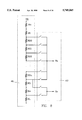
- FIG. 1 is an illustration figure of a conventional digital-to-analog converter which divides voltage segments through the combination of a plurality of R-2R resistors, wherein the reference numerals 10 and 12 denote a multiplex and a buffer respectively.
- the multiplexer 10 shown in FIG. 1 converts the input to switch control codes, i.e. digital signals, and outputs the switch control codes to control the switches. Additionally, FIG.
- FIG. 2 is an illustration figure of another conventional digital-to-analog converter dividing voltage segments through a plurality of resistors connected in series, wherein the reference numeral 11 is a multiplexer having the same function as the multiplexer 10 in FIG. 1 and the reference numeral 14 is a buffer.
- the reference numeral 11 is a multiplexer having the same function as the multiplexer 10 in FIG. 1
- the reference numeral 14 is a buffer.
- FIG. 2 it is necessary to generate 50 sets of corresponding codes first in order to obtain an analog signal of 50 stages.
- resistors and switches are necessary so that the analog signal output can be obtained from the conversion of corresponding codes.
- switches and resistor segments for example, the serial-resistor voltage-dividing type of digital to analog converter as shown in FIG.
- the R-2R type circuit the characteristics of the elements will effect the precision of R-2R network due to the currents flowing through the switches. While CMOS, PMOS or NMOS elements are utilized as switches, the currents through the MOS elements will be shifted due to the resistive characteristics varying with the change in voltage and temperature so that the output signals of the R-2R network are distorted. Generally speaking, in dividing voltage segments, the precision of R-2R network is worse than that of the serial resistors. And, for the same number of bits utilized, the resistor value and the area MOS occupied in the R-2R network are both much higher than those of the serial-resistor type.
- a traditional digital to analog converter needs a great amount of elements, occupies large circuit area and needs a more complicated circuit to achieve the determined precision. Therefore, the cost increases and the precision effect factors become more difficult to control due to the increasement in the number of elements and the complexity in circuit design.
- an improved multiple voltage level generation circuit is provided instead of a conventional divided-step voltage output circuit.
- the multiple voltage level generation circuit is composed by a divided-step voltage output circuit and a level-voltage output circuit wherein the two voltage output circuits may be achieved by lots of different implementations.
- a conventional circuit composed by a 7-bit R-2R network can be modified into a circuit combined by a 5-bit R-2R divided-step voltage output circuit and a 2-bit R-2R level voltage output circuit.
- the improved multiple voltage generation circuit composed by a divided-step voltage output circuit and a level-voltage output circuit is further modified under the same design principle.
- the difference is that the divided-step voltage output circuit and the level-voltage output circuit are respectively modified into a divided-step current output circuit and a level-current output circuit.
- the current output signals are then converted into voltage output signals.
- an output voltage signal is derived.
- the level-shift type digital to analog converters disclosed in the foregoing two embodiments are adapted to operate precisely under smaller voltage range.
- a large power supply voltage V DD range is necessary.
- the digital to analog converter should add a stabilization circuit to stabilize the DC and AC values. Therefore, the inventor further provides a third embodiment for being applied to a larger power supply voltage V DD range.
- the objects of the first and the second embodiments of this invention are to provide the voltage output values in need with a divided-step voltage/current output circuit and a level voltage/current output circuit to generate the demanded voltage output value.
- Such an architecture may solve the problems in conventional digital to analog converter design due to a large number of circuit elements utilized and the complexity, such as noise caused by environments, the difficulty in controlling the precision, and the burden in manufacturing cost, etc. With the embodiments disclosed in this present invention, both the manufacturing cost and the complexity of the circuit design are decreased a lot.
- Another object of the first embodiment of this present invention is to provide the demanded output voltage signal with a level-shift type buffer circuit for processing the voltage values output from the divided-step voltage output circuit and the level-voltage output circuit.
- Another object of the second embodiment of this present invention is to provide the demanded output voltage signal with a converting circuit for converting the current signals output from the divided-step current output circuit and a level-current output circuit to voltage signals and then with a level-shift type buffer circuit for processing the foregoing voltage signals output from the converting circuit.
- the objects of the third embodiment of this invention is to provide a circuit implemented in a larger power supply voltage V DD range.
- the circuit architecture of the third embodiment combines the level voltage generation circuit and the divided-step voltage generation circuit to a multiple voltage level generation circuit and then, utilizes a voltage level selection circuit inside a selection circuit to provide level voltage input and divided-voltage input to a level-shift type buffer circuit.
- FIG. 1 is a diagram illustrating a conventional digital to analog converter.
- FIG. 2 is a diagram illustrating another conventional digital to analog converter.
- FIG. 3 is a circuit block diagram of the first embodiment according to this present invention.
- FIG. 4 is a circuit diagram of the level-shift type buffer stage circuit of the first embodiment according to this present invention.
- FIG. 5 is a circuit block diagram of the second embodiment according to this present invention.
- FIG. 6 is a diagram illustrating the output voltage generated by the second embodiment according to this present invention.
- FIG. 7 is a circuit block diagram of the third embodiment according to this present invention.
- FIG. 8 illustrates the internal circuits and the connection relation between the voltage selection circuit and the multiple voltage level generation circuit shown in FIG. 7.
- FIG. 9A shows the circuit diagram according to another embodiment of the level-shift type buffer stage circuit.
- FIG. 9B and 9C illustrate the circuit diagrams of the power supply follower of the input stage shown in FIG. 9A.
- FIG. 10A illustrates the stabilization circuit diagram according to the first example of the third embodiment of the present invention.
- FIG. 10B shows the circuit diagram according to an embodiment of this present invention, which illustrates that the voltage V BG provided to the device providing bandgap reference of fixed value, is derived from the difference between the output voltages V 0 and V SS .
- FIG. 10C shows the circuit diagram according to another embodiment of this present invention, which illustrates that the voltage V BG provided to the device providing bandgap reference of fixed values, is derived from the difference between the output voltages V O and V SS .
- FIG. 10D shows a second example of the stabilization circuit diagram according to the third embodiment of this present invention.
- FIG. 10E illustrates the circuit for increasing the stability of the stabilization circuit according to the third embodiment of this present invention.
- FIG. 10F is an exemplary circuit diagram of an operational amplifier.
- FIG. 10G is a third example of the stabilization circuit diagram according to the third embodiment of this present invention.
- FIG. 10H shows a plurality of other exemplary bias circuits, which are used in FIG. 10G, composed by a switch element SW and registers R1 and R2.
- FIG. 11A through FIG. 11D show kinds of switch circuits utilized in the switch elements shown in FIG. 10.
- FIG. 3 is the circuit block diagram according to the first embodiment of this present invention, which includes a selection circuit 20, a multiple voltage level generation circuit 21, a level-shift type buffer stage circuit 24.
- the multiple voltage level generation circuit is composed by a divided-step voltage output circuit 22 and a level voltage output circuit 23.
- the divided-step voltage output circuit 26 and the level voltage output circuit 28 the number of voltage steps, the number of levels and the voltage difference at each step can be respectively designed and planned by user.
- V n (S) is the output voltage value of the divided-step voltage output circuit wherein S is the number of the steps;
- V e (X) is the output voltage value of the level voltage output circuitwherein X is the number of the levels;
- O/P is the final output voltage value of the synthesized circuit of the divided-step voltage output circuit and the level voltage output circuit.
- the step voltage difference from the step voltage output circuit is thendetermined as 0.1V, and the level voltage difference of the level voltage output circuit is IV. Therefore, the following equations are obtained:
- V n (S) 0.1V ⁇ S
- V e (X) 1V ⁇ X.
- the selection circuit 20 converts the original digital values to the digital codes for the digital to analog converter, and then respectively output the digital code signals to the step voltage output circuit 22 and the level voltage output circuit 23.
- the divided-step voltage output circuit 22 and the level voltage output circuit 23 respectively output a voltage signal to the level shift type buffer stage circuit 23 according to the input signal from the selection circuit 20, the predetermined number of steps, the predetermined number oflevels, and the voltage differences at each step and each level.
- the level-shift type buffer stage 23 further processes the voltage signals as described in the following paragraphs and then outputs the analog voltage output signals.
- V O (1+R2/R1) V nAC + (1+R2/R1)V nDC -(R2/R1)V eDC !, wherein (1+R2/R1) V nAC is an alternate current signal and (1+R2/R1)V nDC -(R2/R1)V eDC ! is a direct current signal. Therefore, through adjustment of the resistor values R1 and R2 and the voltage signal value V e output from the level voltage output circuit, the output voltage V o is obtained.
- FIG. 5 shows the circuit block diagram according to the second embodiment of this present invention, which includes a selection circuit 30, a multi-current generation circuit 31, a current/voltage conversion circuit 35 and a buffer stage circuit 34.
- the multi-current generation circuit 31 is composed by a divided-step current output circuit 32 and a level current output circuit 33.
- the operations regarding the demanded numbers of steps and levels respectively generated by the divided-step current output circuit 32 and the level current output circuit 36 are not redundantly described here since the principle of the operations are the same as described above in the first embodiment of this present invention.And, the demanded output voltage O/P generated in this second embodiment ofthis present invention is illustrated below referring to FIG. 6 and the related parameters are defined as follows:
- IL(a) the current value output from the level current circuit, a:the numberof levels
- Is(b) the current value output from the divided-step current circuit, b:thenumber of steps;
- the current value difference at each level of the level current output circuit is defined as ⁇ I L and, the current value difference at each step of the step current output circuit is ⁇ I S , equal to ⁇ I L /10.
- the divided-step current output circuit 32 and the level current output circuit 33 respectively output a current signal to the current/voltage conversion circuit 35 according to the predetermined levels, steps, the current value difference at each step andthe current value difference at each level.
- the current/voltage conversion circuit 35 converts the combined current values to voltage values and thenoutput to the buffer stage circuit 34.
- the buffer stage circuit 34 further processed the voltage values and then output the demanded analog voltage output signal.
- the third embodiment of this present invention includes a selection circuit 40, a multiple voltage level generation circuit 41, a stabilization circuit 45 and a level-shift type buffer stagecircuit 44.
- the selection circuit is composed by a decoder 42 and a voltagelevel selection circuit 43.
- the decoder receives digital output signals I/Pfirst and then converts the signals I/P to the signals of a format receivable by the voltage level selection circuit 43.
- the voltage level selection circuit 43 receives the signals from the multiple voltage level generation circuit 41 composed by a decoder 42, a level voltage generationcircuit and a divided -step voltage generation circuit.
- the voltage level selection circuit 43 then outputs the appropriate divided-step voltage output value and the level voltage output value Ve for being provided to the level-shift type buffer stage circuit 44.
- the circuit 41 is utilized to generate multiple voltage levels for voltage selection.
- the stabilization circuit 45 is provided for generating at least an insensitive reference voltage or an insensitive reference currentso that other components may use.
- FIG. 8 illustrates the internal diagram and the connection way of the voltage level selection circuit 43 and the multiple voltage level generation circuit 41 as shown in FIG. 7.
- the multiple voltage level generation circuit 41 for generating a plurality of voltages of different levels includes a serial circuit composed by a plurality of resistors connected in series. The two terminals of the serial circuit is connected between a high voltage potential and a low voltage potential wherein ##EQU1##
- the resistor values of RH and RL can be adjusted appropriately to control the AC and DC values.
- the number of the levels is two and the output is amplified two times.
- the voltage level selection circuit43 includes a plurality of switch elements wherein the on/off status is controlled by a decoder so that the output terminal can output the divided-step voltage output values and the level voltage output values in demand.
- FIG. 9A shows the circuit diagram of another embodiment of the level-shift type of buffer circuit.
- the circuit structure shown in FIG. 9A is mainly the same as the circuit shown in FIG. 4. The difference is in that the input portion of the divided-step voltage output value V n and the level voltage output value V e respectively includes an input stage circuit composed by two PMOS elements.
- FIG. 9B shows the circuit diagram of a source follower utilized as the above-mentioned input stage circuit.
- FIG. 9C illustrates the circuit diagram of a source follower composed by NMOS transistors.
- FIG. 10A to FIG. 10F show different examples of the stabilization circuit 45 according to this present invention.
- FIG. 10A shows the first example of the stabilization circuit (45) according to this present invention.
- This example includes a bandgap-reference element 451 and a PMOS element 452.
- This circuit utilizes the fixed reference of the bandgap to form a stable voltage level V BG which does not vary with V DD .
- V BG could be different as the process variation, and usually the value of V BG is within the range 1.2V to 1.3V.
- FIG. 10B shows the circuit diagram that V BG is the difference of the output voltage V O and V SS .
- FIG. 1OC shows the circuit diagram that V BG is the difference of the output voltage V O and V DD .
- the current I Ref is a fixed value which is a constant current source. With a current mirror for example, the constant current source canbe fetched for reference.
- FIG. 10D is the circuit diagram of the second example of the stabilization circuit 45 of this present invention wherein the self-bias reference technique is used.
- the PMOS elements M1, M2, M3 and M4 comprise a self-bias reference current source circuit for reducing power consumption at power-down state and, M sp and M sn are respectively controlledby the control reference voltage Vcon and its inverse voltage /Vcon.
- the reference current Iref is an insensitive current reference source, wherein a current mirror can be obtained through the connection of the output voltage V P to the gate of the PMOS of the connection of V N to the gate of the NMOS.
- a stable current source is obtained.
- the output voltage V P can be fetched to be connected to the circuit in FIG. 10, and then the output value V N' isutilized to compose a current mirror. Therefore, in the circuit diagram shown in FIG. 10E, for increasing the stability of the stabilization circuit according to the embodiment of this present invention, if there are MOS elements M x connected in the circuit, this type of circuit isespecially adapted to a buffer stage circuit composed by a source follower as illustrated in FIG. 9; if the MOS elements M X are deleted from thecircuit, this type of circuit is especially adapted to a buffer stage circuit composed by operational amplifiers as illustrated in FIG. 4. FIG.
- V N , V N' or V P applied to the current source of the operational amplifier or the source follower of the output buffer stage as shown in FIG. 4 or 9A can be connected as a current mirror so that the characteristics of the operational amplifier or the source follower will not vary with V DD a lot.
- the above-mentioned stabilization circuit can be further improved.
- the difference between V H and V L is the emitter-base voltage V BE of the transistorQ1, which is a constant voltage source for the voltage input provided to the multiple voltage level generation circuit 41 shown in FIG. 1.
- the peak-to-peak output voltage value V p-p is thus stabilized and, the voltage level V bias , instead of the V N' as the example discussedin the last paragraph, can be used as the bias voltage source of the current source of the operational amplifier.
- the voltage levels are connected to the two terminals, correspondingly marked as the symbols V H and V L , of the serial resistors of the multiple voltage level generation circuit 41 shown in FIG. 8.
- This circuit can maintain the stabilization of the DC voltage level so that the DC voltage will not exceed the permitted error range dueto the current variation flowing through the transistors.
- the current flowing through the transistors is affected by the variation line process parameters, shift, temperature, etc.
- FIG. 10H there are a lot of different combination ways for the bias voltage V L circuit design composed by the switch elementSW and the resistors R1 and R2.
- the switch element SW can be implemented inmany different ways as examplarily shown in FIG. 11A through FIG. 11D, wherein FIG. 11A is a PMOS switch circuit, FIG. 11B is a NMOS switch circuit, FIG. 11C is a CMOS switch circuit and FIG. 11D is an analog switch circuit.
- the analog switch circuit as shown in FIG. 11D is implemented on the P-well process. That is to say, the NMOS substrate is connected to the two terminals X1 and X2 of the switch while the analog switch is turned on and, connected to V DD while the analog switch is turned off.
- the level-shift type digital-to-analog converter according to this present invention has the following advantages.
- This present invention provides higher precision with the same circuit complexity. That is to say, this present invention provides the same precision as the conventional circuit with much simpler circuit.
- This present invention reduces the circuit complexity and the number ofelements utilized of a conventional circuit. It is useful for the precisioncontrol and the interference from the surroundings can be reduced therefore.
- This present invention reduces the number of switch elements utilized so that the noise caused by switching the switches is effectively reduced.
- This present invention greatly reduces the number of elements utilized so that the manufacture cost is decreased.
Abstract
Description
3.5V=V.sub.n (5)+V.sub.e (3)
0.8V=V.sub.n (8)+V.sub.e (0).
I.sub.L (z+1)=I.sub.L (z)+ΔI.sub.L, z=0, 1, 2, 3, 4;
I.sub.S (w+1)=I.sub.S (w)+ΔI.sub.S, w=0, 1, 2, 3, . . . , 7, 8
Claims (10)
Priority Applications (1)
| Application Number | Priority Date | Filing Date | Title |
|---|---|---|---|
| US08/826,694 US5745065A (en) | 1997-04-07 | 1997-04-07 | Level-shift type digital to analog converter |
Applications Claiming Priority (1)
| Application Number | Priority Date | Filing Date | Title |
|---|---|---|---|
| US08/826,694 US5745065A (en) | 1997-04-07 | 1997-04-07 | Level-shift type digital to analog converter |
Publications (1)
| Publication Number | Publication Date |
|---|---|
| US5745065A true US5745065A (en) | 1998-04-28 |
Family
ID=25247275
Family Applications (1)
| Application Number | Title | Priority Date | Filing Date |
|---|---|---|---|
| US08/826,694 Expired - Fee Related US5745065A (en) | 1997-04-07 | 1997-04-07 | Level-shift type digital to analog converter |
Country Status (1)
| Country | Link |
|---|---|
| US (1) | US5745065A (en) |
Cited By (3)
| Publication number | Priority date | Publication date | Assignee | Title |
|---|---|---|---|---|
| US6118262A (en) * | 1999-05-13 | 2000-09-12 | Fujitsu Limited | Voltage generating circuit and D/A converter |
| US6344815B2 (en) * | 1999-10-14 | 2002-02-05 | Oki Electric Industry Co., Ltd. | Digital-to-analog converter |
| US6356222B1 (en) * | 2000-05-04 | 2002-03-12 | Matsushita Mobile Communication Development Corporation Of Usa | Circuit to increase the precision of a digital-to-analog converter |
Citations (2)
| Publication number | Priority date | Publication date | Assignee | Title |
|---|---|---|---|---|
| US4607249A (en) * | 1985-05-08 | 1986-08-19 | Bbrr-Brown Corporation | Input level shifting circuit for low voltage digital-to-analog converter |
| US5079552A (en) * | 1990-01-11 | 1992-01-07 | U.S. Philips Corporation | Digital-to-analog converter |
-
1997
- 1997-04-07 US US08/826,694 patent/US5745065A/en not_active Expired - Fee Related
Patent Citations (2)
| Publication number | Priority date | Publication date | Assignee | Title |
|---|---|---|---|---|
| US4607249A (en) * | 1985-05-08 | 1986-08-19 | Bbrr-Brown Corporation | Input level shifting circuit for low voltage digital-to-analog converter |
| US5079552A (en) * | 1990-01-11 | 1992-01-07 | U.S. Philips Corporation | Digital-to-analog converter |
Cited By (3)
| Publication number | Priority date | Publication date | Assignee | Title |
|---|---|---|---|---|
| US6118262A (en) * | 1999-05-13 | 2000-09-12 | Fujitsu Limited | Voltage generating circuit and D/A converter |
| US6344815B2 (en) * | 1999-10-14 | 2002-02-05 | Oki Electric Industry Co., Ltd. | Digital-to-analog converter |
| US6356222B1 (en) * | 2000-05-04 | 2002-03-12 | Matsushita Mobile Communication Development Corporation Of Usa | Circuit to increase the precision of a digital-to-analog converter |
Similar Documents
| Publication | Publication Date | Title |
|---|---|---|
| KR100186679B1 (en) | Digital-to-analog converter | |
| US5283579A (en) | Digital to analog converter having high multiplying bandwidth | |
| US7068201B1 (en) | Digital-to-analog converter | |
| EP1257060B1 (en) | Digital-to-analogue converter using an array of current sources | |
| US5790060A (en) | Digital-to-analog converter having enhanced current steering and associated method | |
| US6603417B2 (en) | CMOS DAC with high impedance differential current drivers | |
| US5801655A (en) | Multi-channel D/A converter utilizing a coarse D/A converter and a fine D/A converter | |
| US6703956B1 (en) | Technique for improved linearity of high-precision, low-current digital-to-analog converters | |
| US5798723A (en) | Accurate and precise current matching for low voltage CMOS digital to analog converters | |
| EP2366221B1 (en) | Amplifier with dither | |
| KR20050026172A (en) | Current-added-type digital to analog converter and digital to analog converting method thereof | |
| US20060066463A1 (en) | High resolution and low consumption digital-to-analog converter | |
| KR100494202B1 (en) | A/D converter | |
| US5592167A (en) | Analog-digital converter using current controlled voltage reference | |
| US20070262893A1 (en) | Techniques for biasing a radio frequency digital to analog converter | |
| US20010026236A1 (en) | Digital-to-analog converter | |
| US11303294B2 (en) | Digital to analog converters | |
| US5745065A (en) | Level-shift type digital to analog converter | |
| JP2001044837A (en) | Digital/analog converting circuit and analog/digital converting circuit using the same | |
| US7277036B2 (en) | Digital-to-analog converting circuit | |
| JP2002050966A (en) | Da converter | |
| KR100792708B1 (en) | Digital analog converter | |
| WO2007147891A1 (en) | Digital-to-analog converter with controlled buffered inputs | |
| US7903011B2 (en) | Differential current-mode translator in a sigma-delta digital-to-analog converter | |
| JP4382130B2 (en) | A / D converter |
Legal Events
| Date | Code | Title | Description |
|---|---|---|---|
| AS | Assignment |
Owner name: HOLTEK MICROELECTRONICS, INC., TAIWAN Free format text: ASSIGNMENT OF ASSIGNORS INTEREST;ASSIGNOR:WU, RONG-TYAN;REEL/FRAME:008479/0132 Effective date: 19970327 |
|
| AS | Assignment |
Owner name: UTEK SEMICONDUCTOR CORP., TAIWAN Free format text: CHANGE OF NAME;ASSIGNOR:HOLTEK MICROELECTRONICS, INC.;REEL/FRAME:009490/0001 Effective date: 19980630 |
|
| AS | Assignment |
Owner name: HOLTEK SEMICONDUCTOR INC., TAIWAN Free format text: ASSIGNMENT OF ASSIGNORS INTEREST;ASSIGNOR:UTEK SEMICONDUCTOR CORP.;REEL/FRAME:009822/0606 Effective date: 19981211 |
|
| FEPP | Fee payment procedure |
Free format text: PAT HOLDER CLAIMS SMALL ENTITY STATUS - SMALL BUSINESS (ORIGINAL EVENT CODE: SM02); ENTITY STATUS OF PATENT OWNER: SMALL ENTITY |
|
| FPAY | Fee payment |
Year of fee payment: 4 |
|
| FPAY | Fee payment |
Year of fee payment: 8 |
|
| REMI | Maintenance fee reminder mailed | ||
| LAPS | Lapse for failure to pay maintenance fees | ||
| STCH | Information on status: patent discontinuation |
Free format text: PATENT EXPIRED DUE TO NONPAYMENT OF MAINTENANCE FEES UNDER 37 CFR 1.362 |
|
| FP | Lapsed due to failure to pay maintenance fee |
Effective date: 20100428 |