US5739593A - Voltage source circuit for generating a plurality of values of voltages - Google Patents
Voltage source circuit for generating a plurality of values of voltages Download PDFInfo
- Publication number
- US5739593A US5739593A US08/753,425 US75342596A US5739593A US 5739593 A US5739593 A US 5739593A US 75342596 A US75342596 A US 75342596A US 5739593 A US5739593 A US 5739593A
- Authority
- US
- United States
- Prior art keywords
- terminal
- semiconductor
- mos transistors
- voltage
- gate
- Prior art date
- Legal status (The legal status is an assumption and is not a legal conclusion. Google has not performed a legal analysis and makes no representation as to the accuracy of the status listed.)
- Expired - Lifetime
Links
Images


Classifications
-
- G—PHYSICS
- G09—EDUCATION; CRYPTOGRAPHY; DISPLAY; ADVERTISING; SEALS
- G09G—ARRANGEMENTS OR CIRCUITS FOR CONTROL OF INDICATING DEVICES USING STATIC MEANS TO PRESENT VARIABLE INFORMATION
- G09G3/00—Control arrangements or circuits, of interest only in connection with visual indicators other than cathode-ray tubes
- G09G3/20—Control arrangements or circuits, of interest only in connection with visual indicators other than cathode-ray tubes for presentation of an assembly of a number of characters, e.g. a page, by composing the assembly by combination of individual elements arranged in a matrix no fixed position being assigned to or needed to be assigned to the individual characters or partial characters
- G09G3/34—Control arrangements or circuits, of interest only in connection with visual indicators other than cathode-ray tubes for presentation of an assembly of a number of characters, e.g. a page, by composing the assembly by combination of individual elements arranged in a matrix no fixed position being assigned to or needed to be assigned to the individual characters or partial characters by control of light from an independent source
- G09G3/36—Control arrangements or circuits, of interest only in connection with visual indicators other than cathode-ray tubes for presentation of an assembly of a number of characters, e.g. a page, by composing the assembly by combination of individual elements arranged in a matrix no fixed position being assigned to or needed to be assigned to the individual characters or partial characters by control of light from an independent source using liquid crystals
- G09G3/3611—Control of matrices with row and column drivers
- G09G3/3696—Generation of voltages supplied to electrode drivers
Definitions
- the present invention relates to a multivalued voltage source circuit.
- An integrated circuit producing a plurality of voltages has been widely used for driving/controlling various equipment.
- a display element such as a liquid crystal display, electroluminescent display and a plasma display.
- the number of operational amplifiers is increased in accordance with the number of voltages to be output, resulting in an increase of the dissipated power and the occupied area. For this reason, the monolithic integration is difficult.
- the present invention has been developed in view of the above drawbacks and its object is to provide a voltage source circuit which is capable of producing a number of voltages with a constant output impedance and adapted to be implemented by an integrated circuit.
- a multivalued voltage source circuit comprises: a first terminal; a second terminal; n resistors (n is an integer of two or more) for dividing a voltage applied between the first and second terminals; and (n+1) MOS transistors drains of which are commonly connected, gates of which are connected in one-to-one correspondence to the first terminal, the second terminal, and (n-1) nodes of the n resistors, and sources of which produce output voltages.
- FIG. 1 is a circuit diagram of a multivalued voltage source circuit according to a first embodiment of the present invention
- FIG. 2 is a view showing a backgate bias characteristics of an NMOS transistor used in the embodiment of FIG. 1;
- FIG. 3 is a cross sectional view of an integrated semiconductor circuit with a silicon on sapphire structure which can be used for integrating multivalued voltage source circuits according to the first and second embodiments of the present invention
- FIG. 4 is a cross sectional view of an integrated circuit with an epitaxial structure which can be used for integrating multivalued voltage source circuits according to the first and second embodiments of the present invention
- FIG. 5 is a detailed circuit diagram of the multivalued voltage source circuit shown in FIG. 1;
- FIG. 6 is a circuit diagram of a multivalued voltage source circuit according to a second embodiment of the present invention.
- FIG. 7 is a circuit diagram of a multivalued voltage source circuit according to a third embodiment of the present invention.
- FIG. 8 is a cross sectional view of a CMOS integrated circuit which can be used for implementing the multivalued voltage source circuit according to the third embodiment of the present invention.
- a multivalued voltage source circuit according to the present invention will now be described.
- a multivalued voltage source circuit 50 comprises: resistors 1 comprised of n series-connected division resistors R1, R2, . . . , R(n-1), and Rn; and MOS transistors 2 comprised of (n+1) MOS transistors Q1, Q2, . . . , Qn, Q(n+1).
- the resistors 1 are connected between a first terminal 4 and a second terminal 5.
- Voltages V1 and V2 from externally provided voltage sources 31 and 32 are applied to the first terminal 4 and the second terminal 5, respectively.
- the resistors 1 divide a voltage applied between the first terminal 4 and the second terminal 5.
- a voltage at the first terminal 4, a voltage at the second terminal 5, and voltages at (n-1) nodes between division resistors R1 through Rn are applied, as a gate bias voltage, to corresponding MOS transistors Q1 through Q(n+1), respectively.
- Each drain electrode of the MOS transistors Q1 through Q(n+1) is connected to a drain terminal 3.
- a voltage Vvs is given to the drain terminal 3 from an external voltage source 30.
- (n+1) output voltages Vo1, Vo2, . . . , Von, Vo(n+1) are output from the source electrodes of the MOS transistors Q1 through Q(n+1), respectively.
- Substrate regions of NMOS transistors constituting the MOS transistors 2 are shortcircuited with the source electrodes of the MOS transistors, respectively.
- FIG. 1 shows a state wherein load resistors 6 comprised of (n+1) load resistors RL1 through RL(n+1) are connected to the MOS transistors Q1 through Q(n+1) for explaining that a multivalued voltage source circuit 50 drives various loads.
- each of the resistors RL1 through RL(n+1) is connected to the source electrodes of the MOS transistors Q1 through Q(n+1), respectively and other terminals thereof are commonly grounded.
- the MOS transistors 2 comprises n-channel MOS transistors Q1 through Q(n+1) (hereinafter referred to as NMOS transistors) each having the same threshold voltage Vth.
- a supply voltage of the voltage source 31 is denoted as V1; a supply voltage of the voltage source 32, V2; a supply voltage of the voltage source 30, Vvs; and a resistance value of each division resistors R1 through Rn, r. Furthermore, the resistance value of each of the load resistors RL1 through RL(n+1) is assumed to be smaller than the off resistance value of the MOS transistors Q1 through Q(n+1), and larger than the on resistance value of the MOS transistors Q1 through Q(n+1).
- Ro and Rn are assumed to represent the second terminal 5 and the first terminal 4, respectively, and the voltages Vto and Vtn are assumed to represent the voltage V2 of the second terminal 5 and the voltage V1 of the first terminal 4, respectively.
- a node between the division resistor Ri and the division resistor R(i+1) is connected to the gate electrode of the MOS transistor Q(i+1). Since the voltage at the gate terminal of the MOS transistor Q(i+1) is Vti and its threshold voltage is Vth, the voltage Vo(i+1) at the source terminal (output terminal) raises up to (Vti-Vth) and thereafter the MOS transistor Q(i+1) is turned off if Vvs is higher than (Vti-Vth). More specifically, the voltage Vo(i+1) at the source terminal (output terminal) of the MOS transistor Q(i+1) is expressed by equation (2).
- Vvs, Vth, V1, and V2, and n can be set by adjusting Vvs, Vth, V1, and V2, and n.
- a DC current value flowing into the resistors 1 can be controlled by changing the resistance value of each division resistors R1 through Rn. Accordingly, power dissipated by the resistors 1 can be set to a desired value as needed.
- all the division resistors R1 through Rn have the same resistance value r; all the MOS transistors Q1 through Q(n+1) have the same threshold voltage Vth, and the threshold voltage Vth is not changed with respect to an application of the backgate voltage.
- a number of semiconductor integrated circuits adapted to these states exist as is described later.
- the same type of MOS transistors on a semiconductor integrated substrate have the same threshold voltage.
- one of p-channel and n-channel MOS transistors uses the common substrate as a substrate region (a channel region). For this reason, it is known that changing the source potential of the MOS transistor using the common substrate as the channel region will change the threshold voltage of the MOS transistor due to the so-called backgate bias effect. Operation of the multivalued voltage source circuit shown in FIG. 1 will now be described from a view point of the above situations.
- the backgate bias of the NMOS transistor Q1 is also 8V.
- the output voltage Vo2 is assumed to be 7.6V
- the backgate bias voltage of the NMOS transistor Q2 results in 7.6V.
- Vt2 9.91V
- Vt3 9.45V
- Vt4 8.99V
- Vt5 8.52V
- Vt6 8.06V
- Vt7 7.59V
- Vt8 7.12V
- Vt9 6.65V
- Vt10 6.17V
- Vt11 5.69V
- Vt12 5.20V
- Vt13 4.72V
- Vt14 4.22V
- the output voltage Voi can arbitrarily set by appropriately setting the values of the Vvs, Vt, V1, V2, n and resistance values r1 through rn of the division resistors R1 through Rn.
- a desired voltage value can be produced from the terminal Voi of the circuit shown in FIG. 1 by using the MOS transistors and the resistors integrated in a monolithic fashion.
- FIG. 3 shows a cross section of a first example of the semiconductor integrated circuit constituting the multivalued voltage source circuit shown in FIG. 1.
- the semiconductor integrated circuit shown in FIG. 3 is a semiconductor integrated circuit with a silicon on sapphire structure, and comprises a sapphire substrate 7; and an NMOS transistor 8, a resistor 9 and a PMOS transistor 10 formed on the sapphire substrate 7 in an island fashion while they are insulator-separated.
- the NMOS transistor 8 comprises an n + region serving as a source region and a drain region; a p-type region 12 serving as the channel region; a gate insulating film 13; a gate electrode 14; an interlayer insulating film 15; and a metal wiring 16 forming a source electrode S, and a drain electrode D, etc.
- the resistor 9 comprises a resistor layer 17 constituted by a semiconductor layer, a metal layer, etc.; an interlayer insulating film 15; and a metal wiring 16.
- the PMOS transistor 10 comprises p + region 18 serving as the source region and the drain region; an n-type region 19 serving as the channel region; a gate insulating film 13; a gate electrode 14; an interlayer insulating film 15; and a metal wiring 16 forming a source electrode S and a drain electrode D, etc.
- FIG. 4 shows a cross section of a second example of the semiconductor circuit of the multivalued voltage source circuit shown in FIG. 1.
- the semiconductor integrated circuit shown in FIG. 4 is a semiconductor integrated circuit with an epitaxial structure and comprises a p-type substrate 20; an n-type epitaxial layer 21 formed on the p-type substrate 20; an NMOS transistor 8 junction-separated by the p-type region 18; a resistor 9; and PMOS transistor 10.
- the NMOS transistor 8 comprises a p-type region 12 serving as the channel region; an n + region 11 formed within the p-type region 12 and serving as the source region and the drain region; a gate electrode 14; an interlayer insulating film 15; and a metal wiring 16 serving as the source and drain electrodes.
- the resistor 9 is formed by a resistor layer 17 (a semiconductor layer, a metal wire, etc.), the interlayer insulating film 15 and the metal wiring 16.
- a multivalued voltage source circuit shown in FIG. 5 is implemented by using the NMOS transistor 8 and the resistor 9 (the PMOS transistor is not used in this embodiment) of the semiconductor integrated circuit with structures shown in FIGS. 3 and 4.
- the multivalued voltage source circuit shown in FIG. 5 can be implemented by using 16 NMOS transistors each having a gate length of 1 ⁇ m, a gate width of 100 ⁇ m, a gate oxide film thickness of 25 nm, a threshold voltage of 1V, and an electron mobility of 600 cm 2 /V/s; 15 resistors each having a resistance value of 100 ⁇ ; and a single voltage source of 12V.
- the first and second terminals 4 and 5 thereof are applied with 10V and 20V, respectively.
- the MOS transistors 2 are formed by an NMOS. However, the MOS transistors 2 may be formed by a PMOS transistors.
- FIG. 6 shows an arrangement of a multivalued voltage source circuit when the MOS transistors 2 are formed by the PMOS.
- the multivalued voltage source circuit shown in FIG. 6 differs from the multivalued voltage source circuit shown in FIG. 5 in that the MOS transistors Q1 through Q15 are formed by the P-channel MOS and the voltages of the voltage sources 30, 31 and 32 have an negative polarity.
- the multivalued voltage source circuit shown in FIG. 6 can be implemented by using the PMOS 10 and the resistor 9 shown in FIGS. 3 and 4.
- the PMOS transistor 10 shown in FIG. 3 comprises a p + region 18 serving as the source region and the drain region, an n-type region 19 serving as the channel region; a gate insulating film 13; a gate electrode 14; an interlayer insulating film 15; and a metal wiring serving as the source electrode S and the drain electrode D, etc.
- the PMOS transistor 10 shown in FIG. 4 comprises a p + region 18; an n-type epitaxial region (channel) 21; a gate insulating film 13; a gate electrode 14; an interlayer insulating film 15; and a metal wiring 16.
- the multivalued voltage source circuit shown in FIG. 6 is implemented by the PMOS transistor and the resistor of the semiconductor integrated circuit with the structures shown in FIGS. 3 and 4. More specifically, the multivalued voltage source circuit shown in FIG. 6 can be implemented by using 16 PMOS transistors each having a gate length of 1 ⁇ m, a gate width of 100 ⁇ m, a gate oxide film thickness of 25 nm, a threshold voltage of -1V, a hole mobility of 300 cm 2 /V/S, 15 resistors each having a value of 100 ⁇ , and a single voltage source of -12V. Sixteen 100 M ⁇ resistors are used for the load resistor.
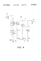
- FIG. 7 shows a circuit diagram according to a third embodiment of the present invention.
- MOS transistors Q1 through Q15 are formed by an N-channel MOS transistors and its backgate is grounded.
- the outputs of the voltage sources 30, 31, and 32 are set to be 12V, 3.72V, and 10.83V, respectively.
- FIG. 8 shows a cross section of the semiconductor integrated circuit usable when the multivalued voltage source circuit shown in FIG. 7 is manufactured.
- the semiconductor integrated circuit shown in FIG. 8 is a CMOS semiconductor integrated circuit with a normal structure and comprises a P-type substrate 20; an NMOS transistor 8; a resistor 9; and a PMOS transistor 10 junction-separated by an n-type well 19.
- the NMOS transistor 8 serves as the source and drain regions and comprises an n + region 11; a p-type substrate region (channel) 20; a gate insulating film 13; a gate electrode 14; an interlayer insulating film 15; and a metal wiring 16 serving as the source and drain electrodes S and D.
- the resistor 9 in FIG. 8 comprises a resistor layer 17 constituted by a semiconductor layer and a metal layer, etc.; an interlayer insulating film 15; and a metal wiring 16.
- the PMOS transistor 10 comprises an n-type well region 19 formed on a p-type substrate 20 and serving as the n-type well region 19; a p + region 18 formed in the n-type well region 19 and serving as the source and drain regions; a gate insulating film 13; a gate electrode 14; an interlayer insulating film 15; a metal wiring 16 serving as the source and drain electrodes S and D.
- the multivalued voltage source circuit shown in FIG. 7 is implemented by using the NMOS transistor 8 and the resistor 9 of the semiconductor circuit with structure shown in FIG. 8. More specifically, the multivalued voltage source circuit shown in FIG. 7 can be implemented by 16 NMOS transistors each having a gate length of 1 ⁇ m, a gate width of 100 ⁇ m, a gate oxide film thickness of 25 nm, a threshold voltage of 1V, an impurity density of 10 16 cm -3 of p-type substrate, a electron mobility of 600 cm 2 /V/s; 15 resistors each having a value of 100 ⁇ , and a single voltage source of 12V. Sixteen 100 M ⁇ resistors are used for the load resistance. The NMOS transistor used has backgate bias dependency shown in FIG. 2.
- the division resistors R1 through Rn all have the same resistance value, resulting in a constant Vdif.
- desired voltages whose Vdif are different at each output terminal may be output by appropriately setting the resistance values of the division resistors R1 through Rn.
- the use of the multivalued voltage source circuits of the above embodiments permits a multivalued voltage with a constant output impedance to be produced with a simple circuit. Furthermore, since a circuit arrangement is simple, a large-size multivalued voltage source circuit for driving various instruments can be integrated in a monolithic fashion. For this reason, various instruments can be manufactured with high performance and low cost.
Landscapes
- Engineering & Computer Science (AREA)
- Chemical & Material Sciences (AREA)
- Crystallography & Structural Chemistry (AREA)
- Physics & Mathematics (AREA)
- Computer Hardware Design (AREA)
- General Physics & Mathematics (AREA)
- Theoretical Computer Science (AREA)
- Semiconductor Integrated Circuits (AREA)
Abstract
Description
Vti=V2-{(V2-V1)/n}·i (1)
Vo(i+1)=Vti-Vth=V2-{(V2-V1)/n}·i-Vth (2)
Vdif=Vo(k)-Vo(k+1)=(V2-V1)/n (3)
Claims (6)
Priority Applications (1)
| Application Number | Priority Date | Filing Date | Title |
|---|---|---|---|
| US08/753,425 US5739593A (en) | 1993-11-29 | 1996-11-25 | Voltage source circuit for generating a plurality of values of voltages |
Applications Claiming Priority (4)
| Application Number | Priority Date | Filing Date | Title |
|---|---|---|---|
| JP5-297167 | 1993-11-29 | ||
| JP5297167A JP2701710B2 (en) | 1993-11-29 | 1993-11-29 | Multi-value voltage source circuit |
| US34707594A | 1994-11-23 | 1994-11-23 | |
| US08/753,425 US5739593A (en) | 1993-11-29 | 1996-11-25 | Voltage source circuit for generating a plurality of values of voltages |
Related Parent Applications (1)
| Application Number | Title | Priority Date | Filing Date |
|---|---|---|---|
| US34707594A Continuation | 1993-11-29 | 1994-11-23 |
Publications (1)
| Publication Number | Publication Date |
|---|---|
| US5739593A true US5739593A (en) | 1998-04-14 |
Family
ID=17843060
Family Applications (1)
| Application Number | Title | Priority Date | Filing Date |
|---|---|---|---|
| US08/753,425 Expired - Lifetime US5739593A (en) | 1993-11-29 | 1996-11-25 | Voltage source circuit for generating a plurality of values of voltages |
Country Status (2)
| Country | Link |
|---|---|
| US (1) | US5739593A (en) |
| JP (1) | JP2701710B2 (en) |
Cited By (6)
| Publication number | Priority date | Publication date | Assignee | Title |
|---|---|---|---|---|
| US5965961A (en) * | 1997-07-26 | 1999-10-12 | Leopold Kostal Gmbh & Co. Kg | Electrical circuit arrangement |
| US20030143796A1 (en) * | 2002-01-17 | 2003-07-31 | Stmicroelectronics Sa | Current or voltage generator with a temperature stable operating point |
| US20040071191A1 (en) * | 2002-08-09 | 2004-04-15 | Jae-Yoon Sim | Temperature sensor and method for detecting trip temperature of a temperature sensor |
| US20050074051A1 (en) * | 2003-10-06 | 2005-04-07 | Myung-Gyoo Won | Temperature sensing circuit for use in semiconductor integrated circuit |
| US20050276144A1 (en) * | 2004-06-14 | 2005-12-15 | Young-Sun Min | Temperature detector providing multiple detected temperature points using single branch and method of detecting shifted temperature |
| US11302696B2 (en) * | 2019-08-26 | 2022-04-12 | Kioxia Corporation | Semiconductor device and method of manufacturing semiconductor device |
Families Citing this family (3)
| Publication number | Priority date | Publication date | Assignee | Title |
|---|---|---|---|---|
| JP2715943B2 (en) * | 1994-12-02 | 1998-02-18 | 日本電気株式会社 | Drive circuit for liquid crystal display |
| JP2833564B2 (en) * | 1996-02-15 | 1998-12-09 | 日本電気株式会社 | Multi-value voltage source circuit |
| CN111477194B (en) * | 2020-05-27 | 2022-02-22 | 京东方科技集团股份有限公司 | Common voltage output circuit, display device and common voltage compensation method |
Citations (14)
| Publication number | Priority date | Publication date | Assignee | Title |
|---|---|---|---|---|
| JPS61116933A (en) * | 1984-11-08 | 1986-06-04 | ロ−ム株式会社 | Power supply circuit |
| US4864162A (en) * | 1988-05-10 | 1989-09-05 | Grumman Aerospace Corporation | Voltage variable FET resistor with chosen resistance-voltage relationship |
| US4924169A (en) * | 1987-12-17 | 1990-05-08 | Dana Corporation | Current regulator for a battery re-charging circuit |
| JPH02228714A (en) * | 1989-03-01 | 1990-09-11 | Fuji Electric Co Ltd | Power source device for multi-voltage output |
| JPH03264922A (en) * | 1990-03-15 | 1991-11-26 | Hitachi Ltd | Visual angle correcting system for multigradation display of liquid crystal and multgradation liquid crystal display device using this system |
| JPH03274089A (en) * | 1990-03-23 | 1991-12-05 | Seiko Epson Corp | liquid crystal display device |
| JPH03274090A (en) * | 1990-03-23 | 1991-12-05 | Seiko Epson Corp | liquid crystal display device |
| JPH0482188A (en) * | 1990-07-25 | 1992-03-16 | Matsushita Electric Ind Co Ltd | Heating cloth |
| JPH04129265A (en) * | 1990-09-20 | 1992-04-30 | Nec Corp | Semiconductor integrated circuit |
| JPH04204689A (en) * | 1990-11-30 | 1992-07-27 | Hitachi Ltd | Driver for multigradation and liquid crystal display device using this driver |
| JPH0524670A (en) * | 1991-06-29 | 1993-02-02 | Minolta Camera Co Ltd | Cover taking-up device |
| US5191277A (en) * | 1989-09-20 | 1993-03-02 | Kabushiki Kaisha Toshiba | Electronic apparatus capable of controlling electric current supply |
| US5362988A (en) * | 1992-05-01 | 1994-11-08 | Texas Instruments Incorporated | Local mid-rail generator circuit |
| US5448190A (en) * | 1993-03-30 | 1995-09-05 | Nec Corporation | Voltage-to-current conversion circuit utilizing mos transistors |
-
1993
- 1993-11-29 JP JP5297167A patent/JP2701710B2/en not_active Expired - Fee Related
-
1996
- 1996-11-25 US US08/753,425 patent/US5739593A/en not_active Expired - Lifetime
Patent Citations (15)
| Publication number | Priority date | Publication date | Assignee | Title |
|---|---|---|---|---|
| JPS61116933A (en) * | 1984-11-08 | 1986-06-04 | ロ−ム株式会社 | Power supply circuit |
| US4924169A (en) * | 1987-12-17 | 1990-05-08 | Dana Corporation | Current regulator for a battery re-charging circuit |
| US4864162B1 (en) * | 1988-05-10 | 1992-10-13 | Grumman Aerospace Corp | |
| US4864162A (en) * | 1988-05-10 | 1989-09-05 | Grumman Aerospace Corporation | Voltage variable FET resistor with chosen resistance-voltage relationship |
| JPH02228714A (en) * | 1989-03-01 | 1990-09-11 | Fuji Electric Co Ltd | Power source device for multi-voltage output |
| US5191277A (en) * | 1989-09-20 | 1993-03-02 | Kabushiki Kaisha Toshiba | Electronic apparatus capable of controlling electric current supply |
| JPH03264922A (en) * | 1990-03-15 | 1991-11-26 | Hitachi Ltd | Visual angle correcting system for multigradation display of liquid crystal and multgradation liquid crystal display device using this system |
| JPH03274090A (en) * | 1990-03-23 | 1991-12-05 | Seiko Epson Corp | liquid crystal display device |
| JPH03274089A (en) * | 1990-03-23 | 1991-12-05 | Seiko Epson Corp | liquid crystal display device |
| JPH0482188A (en) * | 1990-07-25 | 1992-03-16 | Matsushita Electric Ind Co Ltd | Heating cloth |
| JPH04129265A (en) * | 1990-09-20 | 1992-04-30 | Nec Corp | Semiconductor integrated circuit |
| JPH04204689A (en) * | 1990-11-30 | 1992-07-27 | Hitachi Ltd | Driver for multigradation and liquid crystal display device using this driver |
| JPH0524670A (en) * | 1991-06-29 | 1993-02-02 | Minolta Camera Co Ltd | Cover taking-up device |
| US5362988A (en) * | 1992-05-01 | 1994-11-08 | Texas Instruments Incorporated | Local mid-rail generator circuit |
| US5448190A (en) * | 1993-03-30 | 1995-09-05 | Nec Corporation | Voltage-to-current conversion circuit utilizing mos transistors |
Cited By (12)
| Publication number | Priority date | Publication date | Assignee | Title |
|---|---|---|---|---|
| US5965961A (en) * | 1997-07-26 | 1999-10-12 | Leopold Kostal Gmbh & Co. Kg | Electrical circuit arrangement |
| US20030143796A1 (en) * | 2002-01-17 | 2003-07-31 | Stmicroelectronics Sa | Current or voltage generator with a temperature stable operating point |
| US6831503B2 (en) * | 2002-01-17 | 2004-12-14 | Stmicroelectronics Sa | Current or voltage generator with a temperature stable operating point |
| US20040071191A1 (en) * | 2002-08-09 | 2004-04-15 | Jae-Yoon Sim | Temperature sensor and method for detecting trip temperature of a temperature sensor |
| US20050024097A1 (en) * | 2002-08-09 | 2005-02-03 | Jae-Yoon Sim | Temperature sensor and method for detecting trip temperature of a temperature sensor |
| US6937087B2 (en) | 2002-08-09 | 2005-08-30 | Samsung Electronics Co., Ltd. | Temperature sensor and method for detecting trip temperature of a temperature sensor |
| US7106127B2 (en) * | 2002-08-09 | 2006-09-12 | Samsung Electronics Co., Ltd. | Temperature sensor and method for detecting trip temperature of a temperature sensor |
| US20050074051A1 (en) * | 2003-10-06 | 2005-04-07 | Myung-Gyoo Won | Temperature sensing circuit for use in semiconductor integrated circuit |
| US7107178B2 (en) | 2003-10-06 | 2006-09-12 | Samsung Electronics Co., Ltd. | Temperature sensing circuit for use in semiconductor integrated circuit |
| US20050276144A1 (en) * | 2004-06-14 | 2005-12-15 | Young-Sun Min | Temperature detector providing multiple detected temperature points using single branch and method of detecting shifted temperature |
| US7315792B2 (en) | 2004-06-14 | 2008-01-01 | Samsung Electronics Co., Ltd. | Temperature detector providing multiple detected temperature points using single branch and method of detecting shifted temperature |
| US11302696B2 (en) * | 2019-08-26 | 2022-04-12 | Kioxia Corporation | Semiconductor device and method of manufacturing semiconductor device |
Also Published As
| Publication number | Publication date |
|---|---|
| JPH07153914A (en) | 1995-06-16 |
| JP2701710B2 (en) | 1998-01-21 |
Similar Documents
| Publication | Publication Date | Title |
|---|---|---|
| EP0485016B1 (en) | Integrated charge pump circuit with back bias voltage reduction | |
| US6603346B2 (en) | Semiconductor booster circuit having cascaded MOS transistors | |
| KR100274918B1 (en) | Silicon-on-insulator body-coupled gated diode for electrostatic discharge(esd) and analog applications | |
| US7145370B2 (en) | High-voltage switches in single-well CMOS processes | |
| US6208200B1 (en) | Level shift circuit with low voltage operation | |
| US7466189B2 (en) | Semiconductor integrated circuit | |
| KR20000070951A (en) | High-voltage cmos level shifter | |
| TW589797B (en) | Level conversion circuit converting logic level of signal | |
| EP0788684A1 (en) | High voltage level shifter for switching high voltage in non-volatile memory integrated circuits | |
| US4152716A (en) | Voltage dividing circuit in IC structure | |
| US12283952B2 (en) | Voltage level shifter with multi-step programmable high supply voltage and high supply voltage-dependent variable low supply and gate bias voltages | |
| US5739593A (en) | Voltage source circuit for generating a plurality of values of voltages | |
| KR100405647B1 (en) | Level shift circuit and image display device | |
| US6127857A (en) | Output buffer or voltage hold for analog of multilevel processing | |
| US5926064A (en) | Floating MOS capacitor | |
| KR100227583B1 (en) | Semiconductor device | |
| KR19990014027A (en) | Medium Potential Generation Circuit | |
| US11979156B2 (en) | Level shifter | |
| CN100350728C (en) | Transistor circuit and booster circuit | |
| CN101242174B (en) | Semiconductor switch | |
| JPH1168534A (en) | High voltage drive circuit | |
| US8305130B2 (en) | Clamp circuit using PMOS and NMOS devices | |
| US20030222701A1 (en) | Level shifter having plurality of outputs | |
| US4423369A (en) | Integrated voltage supply | |
| JPH1145946A (en) | Semiconductor integrated circuit |
Legal Events
| Date | Code | Title | Description |
|---|---|---|---|
| STCF | Information on status: patent grant |
Free format text: PATENTED CASE |
|
| CC | Certificate of correction | ||
| FEPP | Fee payment procedure |
Free format text: PAYOR NUMBER ASSIGNED (ORIGINAL EVENT CODE: ASPN); ENTITY STATUS OF PATENT OWNER: LARGE ENTITY |
|
| FPAY | Fee payment |
Year of fee payment: 4 |
|
| FPAY | Fee payment |
Year of fee payment: 8 |
|
| FPAY | Fee payment |
Year of fee payment: 12 |
|
| FEPP | Fee payment procedure |
Free format text: PAYER NUMBER DE-ASSIGNED (ORIGINAL EVENT CODE: RMPN); ENTITY STATUS OF PATENT OWNER: LARGE ENTITY Free format text: PAYOR NUMBER ASSIGNED (ORIGINAL EVENT CODE: ASPN); ENTITY STATUS OF PATENT OWNER: LARGE ENTITY |
|
| AS | Assignment |
Owner name: GETNER FOUNDATION LLC, DELAWARE Free format text: ASSIGNMENT OF ASSIGNORS INTEREST;ASSIGNOR:NEC CORPORATION;REEL/FRAME:026254/0381 Effective date: 20110418 |
|
| AS | Assignment |
Owner name: NEC CORPORATION, JAPAN Free format text: ASSIGNMENT OF ASSIGNORS INTEREST;ASSIGNOR:HAYAMA, HIROSHI;REEL/FRAME:026373/0880 Effective date: 19941020 |
|
| AS | Assignment |
Owner name: VISTA PEAK VENTURES, LLC, TEXAS Free format text: ASSIGNMENT OF ASSIGNORS INTEREST;ASSIGNOR:GETNER FOUNDATION LLC;REEL/FRAME:045469/0164 Effective date: 20180213 |