US5611955A - High resistivity silicon carbide substrates for high power microwave devices - Google Patents
High resistivity silicon carbide substrates for high power microwave devices Download PDFInfo
- Publication number
- US5611955A US5611955A US08/138,566 US13856693A US5611955A US 5611955 A US5611955 A US 5611955A US 13856693 A US13856693 A US 13856693A US 5611955 A US5611955 A US 5611955A
- Authority
- US
- United States
- Prior art keywords
- silicon carbide
- matter
- deep level
- vanadium
- resistivity
- Prior art date
- Legal status (The legal status is an assumption and is not a legal conclusion. Google has not performed a legal analysis and makes no representation as to the accuracy of the status listed.)
- Expired - Lifetime
Links
Images
Classifications
-
- C—CHEMISTRY; METALLURGY
- C30—CRYSTAL GROWTH
- C30B—SINGLE-CRYSTAL GROWTH; UNIDIRECTIONAL SOLIDIFICATION OF EUTECTIC MATERIAL OR UNIDIRECTIONAL DEMIXING OF EUTECTOID MATERIAL; REFINING BY ZONE-MELTING OF MATERIAL; PRODUCTION OF A HOMOGENEOUS POLYCRYSTALLINE MATERIAL WITH DEFINED STRUCTURE; SINGLE CRYSTALS OR HOMOGENEOUS POLYCRYSTALLINE MATERIAL WITH DEFINED STRUCTURE; AFTER-TREATMENT OF SINGLE CRYSTALS OR A HOMOGENEOUS POLYCRYSTALLINE MATERIAL WITH DEFINED STRUCTURE; APPARATUS THEREFOR
- C30B23/00—Single-crystal growth by condensing evaporated or sublimed materials
- C30B23/02—Epitaxial-layer growth
-
- C—CHEMISTRY; METALLURGY
- C30—CRYSTAL GROWTH
- C30B—SINGLE-CRYSTAL GROWTH; UNIDIRECTIONAL SOLIDIFICATION OF EUTECTIC MATERIAL OR UNIDIRECTIONAL DEMIXING OF EUTECTOID MATERIAL; REFINING BY ZONE-MELTING OF MATERIAL; PRODUCTION OF A HOMOGENEOUS POLYCRYSTALLINE MATERIAL WITH DEFINED STRUCTURE; SINGLE CRYSTALS OR HOMOGENEOUS POLYCRYSTALLINE MATERIAL WITH DEFINED STRUCTURE; AFTER-TREATMENT OF SINGLE CRYSTALS OR A HOMOGENEOUS POLYCRYSTALLINE MATERIAL WITH DEFINED STRUCTURE; APPARATUS THEREFOR
- C30B29/00—Single crystals or homogeneous polycrystalline material with defined structure characterised by the material or by their shape
- C30B29/10—Inorganic compounds or compositions
- C30B29/36—Carbides
-
- H—ELECTRICITY
- H10—SEMICONDUCTOR DEVICES; ELECTRIC SOLID-STATE DEVICES NOT OTHERWISE PROVIDED FOR
- H10P—GENERIC PROCESSES OR APPARATUS FOR THE MANUFACTURE OR TREATMENT OF DEVICES COVERED BY CLASS H10
- H10P14/00—Formation of materials, e.g. in the shape of layers or pillars
- H10P14/20—Formation of materials, e.g. in the shape of layers or pillars of semiconductor materials
- H10P14/22—Formation of materials, e.g. in the shape of layers or pillars of semiconductor materials using physical deposition, e.g. vacuum deposition or sputtering
-
- H—ELECTRICITY
- H10—SEMICONDUCTOR DEVICES; ELECTRIC SOLID-STATE DEVICES NOT OTHERWISE PROVIDED FOR
- H10P—GENERIC PROCESSES OR APPARATUS FOR THE MANUFACTURE OR TREATMENT OF DEVICES COVERED BY CLASS H10
- H10P14/00—Formation of materials, e.g. in the shape of layers or pillars
- H10P14/20—Formation of materials, e.g. in the shape of layers or pillars of semiconductor materials
- H10P14/34—Deposited materials, e.g. layers
- H10P14/3402—Deposited materials, e.g. layers characterised by the chemical composition
- H10P14/3404—Deposited materials, e.g. layers characterised by the chemical composition being Group IVA materials
- H10P14/3408—Silicon carbide
-
- H—ELECTRICITY
- H10—SEMICONDUCTOR DEVICES; ELECTRIC SOLID-STATE DEVICES NOT OTHERWISE PROVIDED FOR
- H10P—GENERIC PROCESSES OR APPARATUS FOR THE MANUFACTURE OR TREATMENT OF DEVICES COVERED BY CLASS H10
- H10P14/00—Formation of materials, e.g. in the shape of layers or pillars
- H10P14/20—Formation of materials, e.g. in the shape of layers or pillars of semiconductor materials
- H10P14/34—Deposited materials, e.g. layers
- H10P14/3438—Doping during depositing
- H10P14/3441—Conductivity type
- H10P14/3446—Transition metal elements; Rare earth elements
-
- Y—GENERAL TAGGING OF NEW TECHNOLOGICAL DEVELOPMENTS; GENERAL TAGGING OF CROSS-SECTIONAL TECHNOLOGIES SPANNING OVER SEVERAL SECTIONS OF THE IPC; TECHNICAL SUBJECTS COVERED BY FORMER USPC CROSS-REFERENCE ART COLLECTIONS [XRACs] AND DIGESTS
- Y10—TECHNICAL SUBJECTS COVERED BY FORMER USPC
- Y10S—TECHNICAL SUBJECTS COVERED BY FORMER USPC CROSS-REFERENCE ART COLLECTIONS [XRACs] AND DIGESTS
- Y10S148/00—Metal treatment
- Y10S148/148—Silicon carbide
Definitions
- the present invention relates to methods for producing silicon carbide semiconductor substrates having high resistivity.
- Silicon carbide exhibits many attractive electrical and thermophysical properties for the fabrication of high power density solid state devices operating at microwave frequencies.
- Silicon carbide based microwave transistors and integrated circuits may provide approximately five times the power density of gallium arsenide MMICs at X band, and approximately ten times the power density of silicon at UHF to S band frequency.
- silicon carbide is a relatively new technology.
- recent advances in the growth of large diameter silicon carbide substrates and the realization of silicon carbide's superior temperature, thermal conductivity, and electric field breakdown properties have prompted intensive research efforts to develop silicon carbide based electronic materials and devices extensively throughout the industry.
- the silicon carbide devices currently being produced have power gains limited well below their theoretical performance by parasitic conduction and capacitive losses in the substrates. Calculations indicate that 1500 ⁇ -cm substrate resistivity represents a minimum threshold value to achieve RF passive behavior. Also, 5000 ⁇ -cm resistivity is needed to minimize device transmission line losses to 0.1db/cm or less. To ensure device isolation and to minimize backgating effects, resistivities approaching semi-insulating behavior (in the range of 5 ⁇ 10 4 ⁇ -cm or higher) are the goal.
- impurities can be introduced as dopants into semiconductor materials. These incorporated elements give certain properties such as electrical conductivity and conduction type to the semiconductor, respectively. Furthermore, it is known in the art that impurities can be added to some other semiconductor materials to obtain high resistivity characteristics. For example, chromium is doped (incorporated) into gallium arsenide (GaAs) to achieve semi-insulating behavior.
- GaAs gallium arsenide
- techniques used to produce semi-insulating behavior in GaAs are not applicable to silicon carbide, since they rely on introducing the dopant (chromium) by addition to a melt of liquid GaAs at relatively low temperatures (the melting point of GaAs 1238° C. or lower, compared to the growth temperatures for SiC in excess of 2000° C.).
- the process for producing the substrate creates semi-insulating electrical behavior in the substrate by the formation of energy levels lying deep within in the forbidden energy band (band gap) of the silicon carbide.
- these energy levels are referred to as deep levels and consist of energy states lying at least 300 meV away from the conductor or valence band edges.
- very high purity silicon carbide is utilized as the source material.
- the formation of deep levels in the forbidden band involves the controlled introduction of selected elements (either selected heavy metals or passivating elements such as hydrogen, chlorine or fluorine) or combinations of elements into the silicon carbide to form deep level centers in the silicon carbide.
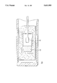
- FIG. 1 shows a schematic of a furnace for producing low loss, high resistivity silicon carbide substrate material.
- the description of the semiconductor material formation will be provided for a single 6H polytype silicon carbide crystal grown by sublimination with the axis of the crystal oriented along the ⁇ 0001> c-direction, it is understood that the process may also be conducted with other polytypes, such as 2H, 4H or 15R and for crystal orientations other than c-axis, such as a-axis ⁇ 1210>. Additionally, chemical vapor deposition (CVD) or other known means may be employed to grow the crystal.
- CVD chemical vapor deposition
- the controlled growth of high purity silicon carbide 6H single crystals is preferably produced in a typical ultra clean (impurity free) physical vapor transport furnace, such as is schematically depicted in FIG. 1. Any heating means such as a resistive heating element may be utilized for heating the furnace.
- An ultra clean environment for crystalline growth is preferably established. The ultra clean environment is obtained by providing hot zone components made using ultra purified graphite and carbon parts or parts consisting of other high purity refractories or coatings.
- a high vacuum pumping system (not shown) may also be employed for high speed degassing of the hot zone components prior to and during growth.
- a silicon carbide sublimation source consisting of feed stock synthesized from high purity Si and C elements (or compounds containing Si and C) is used. Furthermore, ultra pure inert ambient gas such as Ar or He is used during growth as a protective environment in the furnace.
- Deep level elemental impurities are incorporated by introducing these impurities during the high temperature sublimination or CVD growth of the high purity silicon carbide crystals.
- Vanadium and selected other heavy metals introduce a near-mid-band gap energy level.
- non-metallic impurities such as hydrogen, chlorine and fluorine
- the growth of crystals in a chlorine containing ambient can lead to significantly higher as-grown resistivities as well.
- silicon carbide substrate material having high resistivity semi-insulating properties can be formed by incorporating deep level elemental impurities during the sublimation growth of high purity silicon carbide crystals, through systematically introducing candidate elements into the high purity silicon carbide charge or in the form of selected organometallic compounds, as well as by growth in passivating gaseous ambient containing halogens such as chlorine, fluorine or hydrogen.
- the carrier electrons must be excited to a high energy state so they can become mobile and travel through the semiconductor material. Also, in a given semiconductor material only a certain range of energies are available to the carrier electrons, with those energies that are not available being called the energy gap or the forbidden band of the semiconductor. Impurities may be introduced into the semiconductor material such that carrier electrons may occupy various states within the energy band of the semiconductor material.
- the present invention introduces elements into the semiconductor material which create deep levels (energy states within the forbidden energy gap) of the semiconductor. Atoms of the selected impurity create deep levels (energy states) within the forbidden region and can act as trapping centers and compensation centers for the carriers (electrons and holes) of the semiconductor material. By trapping or compensating any mobile carriers, the elemental impurities can cause the material to have a high resistivity and act as a semi-insulator.
- Elements that may act as deep level impurities if incorporated in the semiconductor material include selected "heavy metal" elements from groups IIIB, IVB, VB, VIB, VIIB VIII, IB and IIB from the periodic chart.
- the electronic structure of these elements i.e., being heavier elements having many shells of electrons, makes them potential suitable choices for use as deep level impurities.
- Another group of elements that may be introduced into the semiconductor material during formation of the substrate to achieve high resistivity in the substrate include hydrogen, chlorine, and fluorine.
- hydrogen, chlorine, and fluorine act as electrically passivating impurities for the silicon carbide. Their presence provides electrical activity which compensates electrical activity associated with conducting surface states of the silicon carbide.
- Vanadium was chosen as the dopant element based on the hypothesis that vanadium incorporation in silicon carbide would create deep-level electronic states within the energy gap. These deep-level states could then act as deep donors or acceptors in the compensation of electrically active shallow impurities. The effect of the compensation would be to cause high resistivity (i.e. semi-insulating behavior) in silicon carbide.
- the reduction to practice was carried out in the following way:
- Vanadium-doped silicon carbide single crystals of 6H-polytype were grown in the c- ⁇ 0001>axial direction with diameters up to 50-mm and lengths up to 75-mm using the physical vapor transport (PVT) technique.
- the growth technique utilized a sublimation furnace (FIG. 1) in which high purity graphite materials constituted the hot-zone of the furnace.
- the PVT growth proceeded by sublimation of a vanadium-doped silicon carbide source (held at a temperature of approximately 2300° to 2400° C.) and deposition of the vapor species upon a high quality 6H on carbide monocrystalline seed wafer (held at a temperature of 2100° to 2200° C.).
- the growth rate was controlled by ambient partial pressure, seed to source ⁇ T, and temperature gradient at the solid-vapor interface.
- the growth rate varied between 0.75 and 1.1 mm-hr -1 .
- the crystal was grown in a 20 Torr, high purity Argon ambient provided by the boil-off of ultra-high purity liquid Argon.
- the vanadium-doped silicon carbide used for the sublimation source was prepared in the following way. High purity silicon carbide powder with elemental impurities less than 10 ppm wt. was used as the sublimination source. High purity (99.999%) vanadium metal was mixed with the high purity silicon carbide source powder. In our experiments, the total weight of the source powder was 600 g to which approximately 2.5 g of five nines pure elemental vanadium was added.
- the partial pressure of argon was maintained at 20 Torr; the temperature of the seed was held at 2190° to 2220° C.; the temperature of the subliming vanadium-doped source was held at 2300° to 2350° C.; the seed to source temperature gradient ⁇ T was maintained between 110° and 130° C.
- the resulting vanadium-doped crystal exhibited a vanadium-content between 300 and 1000 ppm wt. as determined by glow discharge mass spectrometry.
- Absorption measurements performed on wafers sliced from the front, middle and end of the crystal show that the vanadium was incorporated uniformly throughout the grown crystal (within a factor of two).
- Differential infrared-absorption measurements further show that the Fermi level is pinned on the vanadium deep-donor level, located at approximately 1 eV below the conduction band edge. The conductivity of the crystal was below the detection limits of conventional measurement equipment.
Landscapes
- Chemical & Material Sciences (AREA)
- Engineering & Computer Science (AREA)
- Crystallography & Structural Chemistry (AREA)
- Materials Engineering (AREA)
- Metallurgy (AREA)
- Organic Chemistry (AREA)
- Inorganic Chemistry (AREA)
- Crystals, And After-Treatments Of Crystals (AREA)
Abstract
Description
Claims (13)
Priority Applications (2)
| Application Number | Priority Date | Filing Date | Title |
|---|---|---|---|
| US08/138,566 US5611955A (en) | 1993-10-18 | 1993-10-18 | High resistivity silicon carbide substrates for high power microwave devices |
| PCT/US1997/001791 WO1998034281A1 (en) | 1993-10-18 | 1997-01-31 | High resistivity silicon carbide substrates for high power microwave devices |
Applications Claiming Priority (2)
| Application Number | Priority Date | Filing Date | Title |
|---|---|---|---|
| US08/138,566 US5611955A (en) | 1993-10-18 | 1993-10-18 | High resistivity silicon carbide substrates for high power microwave devices |
| PCT/US1997/001791 WO1998034281A1 (en) | 1993-10-18 | 1997-01-31 | High resistivity silicon carbide substrates for high power microwave devices |
Publications (1)
| Publication Number | Publication Date |
|---|---|
| US5611955A true US5611955A (en) | 1997-03-18 |
Family
ID=26792333
Family Applications (1)
| Application Number | Title | Priority Date | Filing Date |
|---|---|---|---|
| US08/138,566 Expired - Lifetime US5611955A (en) | 1993-10-18 | 1993-10-18 | High resistivity silicon carbide substrates for high power microwave devices |
Country Status (2)
| Country | Link |
|---|---|
| US (1) | US5611955A (en) |
| WO (1) | WO1998034281A1 (en) |
Cited By (56)
| Publication number | Priority date | Publication date | Assignee | Title |
|---|---|---|---|---|
| WO1998059374A3 (en) * | 1997-06-23 | 1999-03-25 | James Albert Cooper Jr | Insulated gate power semiconductor device having a semi-insulating semiconductor substrate |
| US6177685B1 (en) * | 1998-01-20 | 2001-01-23 | Sharp Kabushiki Kaisha | Nitride-type III-V HEMT having an InN 2DEG channel layer |
| US6218680B1 (en) | 1999-05-18 | 2001-04-17 | Cree, Inc. | Semi-insulating silicon carbide without vanadium domination |
| US6368452B1 (en) | 2000-03-31 | 2002-04-09 | Lam Research Corporation | Plasma treatment apparatus and method of semiconductor processing |
| US6396080B2 (en) | 1999-05-18 | 2002-05-28 | Cree, Inc | Semi-insulating silicon carbide without vanadium domination |
| US20020104478A1 (en) * | 2001-02-07 | 2002-08-08 | Emi Oguri | Silicon carbide single crystal and process for producing the same |
| US6464843B1 (en) | 1998-03-31 | 2002-10-15 | Lam Research Corporation | Contamination controlling method and apparatus for a plasma processing chamber |
| WO2002092886A1 (en) * | 2001-05-11 | 2002-11-21 | Cree Inc. | High-resistivity silicon carbide substrate for semiconductor devices with high breakdown voltage |
| US20030029376A1 (en) * | 2000-03-13 | 2003-02-13 | Snyder David W | Large size single crystal seed crystal fabrication by intergrowth of tiled seed crystals |
| US20030037724A1 (en) * | 2000-03-13 | 2003-02-27 | Snyder David W. | Axial gradient transport appatatus and process for producing large size, single crystals of silicon carbide |
| US20030079676A1 (en) * | 2001-10-29 | 2003-05-01 | Alexandre Ellison | High resistivity silicon carbide single crystal |
| US20030233975A1 (en) * | 2002-06-24 | 2003-12-25 | Cree, Inc. | Method for producing semi-insulating resistivity in high purity silicon carbide crystals |
| US20040155260A1 (en) * | 2001-08-07 | 2004-08-12 | Jan Kuzmik | High electron mobility devices |
| US6780243B1 (en) * | 2001-11-01 | 2004-08-24 | Dow Corning Enterprises, Inc. | Method of silicon carbide monocrystalline boule growth |
| US20040201024A1 (en) * | 2003-04-08 | 2004-10-14 | Tsvetkov Valeri F. | Semi-Insulating Silicon Carbide Produced by Neutron Transmutation Doping |
| US20050022727A1 (en) * | 2003-07-28 | 2005-02-03 | Fechko George J. | Reducing nitrogen content in silicon carbide crystals by sublimation growth in a hydrogen-containing ambient |
| US20050022724A1 (en) * | 2003-07-28 | 2005-02-03 | Malta David Phillip | Growth of ultra-high purity silicon carbide crystals in an ambient containing hydrogen |
| US20050126471A1 (en) * | 2002-06-24 | 2005-06-16 | Jenny Jason R. | One hundred millimeter high purity semi-insulating single crystal silicon carbide wafer |
| US7009209B2 (en) * | 2001-01-03 | 2006-03-07 | Mississippi State University Research And Technology Corporation (Rtc) | Silicon carbide and related wide-bandgap transistors on semi-insulating epitaxy for high-speed, high-power applications |
| US20060075958A1 (en) * | 2004-09-21 | 2006-04-13 | Adrian Powell | Low basal plane dislocation bulk grown SiC wafers |
| EP1652973A1 (en) * | 2004-10-29 | 2006-05-03 | Sixon Ltd. | Silicon carbide single crystal, silicon carbide substrate and manufacturing method for silicon carbide single crystal |
| US20060118037A1 (en) * | 2004-12-08 | 2006-06-08 | Adrian Powell | Process for producing high quality large size silicon carbide crystals |
| US20060174825A1 (en) * | 2005-02-09 | 2006-08-10 | Cem Basceri | Method of forming semi-insulating silicon carbide single crystal |
| US20060213430A1 (en) * | 2002-06-24 | 2006-09-28 | Jenny Jason R | Seeded single crystal silicon carbide growth and resulting crystals |
| US20060225645A1 (en) * | 2005-04-07 | 2006-10-12 | Adrian Powell | Three inch silicon carbide wafer with low warp, bow, and TTV |
| WO2006113657A1 (en) * | 2005-04-19 | 2006-10-26 | Ii-Vi Incorporated | Method of and system for forming sic crystals having spatially uniform doping impurities |
| US20070141823A1 (en) * | 2005-12-12 | 2007-06-21 | Kyma Technologies, Inc. | Inclusion-free uniform semi-insulating group III nitride substrates and methods for making same |
| US20080072817A1 (en) * | 2006-09-26 | 2008-03-27 | Ii-Vi Incorporated | Silicon carbide single crystals with low boron content |
| US20080190355A1 (en) * | 2004-07-07 | 2008-08-14 | Ii-Vi Incorporated | Low-Doped Semi-Insulating Sic Crystals and Method |
| US20080261401A1 (en) * | 2004-04-08 | 2008-10-23 | Ii-Vi Incorporated | Chemical-Mechanical Polishing of Sic Surfaces Using Hydrogen Peroxide or Ozonated Water Solutions in Combination with Colloidal Abrasive |
| US20090053125A1 (en) * | 2007-08-20 | 2009-02-26 | Il-Vi Incorporated | Stabilizing 4H Polytype During Sublimation Growth Of SiC Single Crystals |
| US20090255458A1 (en) * | 2004-12-27 | 2009-10-15 | Nippon Steel Corporation | Silicon carbide single crystal, silicon carbide single crystal wafer, and method of production of same |
| US20100061914A1 (en) * | 2007-01-16 | 2010-03-11 | Ii-Vi Incorporated | GUIDED DIAMETER SiC SUBLIMATION GROWTH WITH MULTI-LAYER GROWTH GUIDE |
| US20100139552A1 (en) * | 2008-12-08 | 2010-06-10 | Ii-Iv Incorporated | Axial Gradient Transport Growth Process and Apparatus Utilizing Resistive Heating |
| US20100159182A1 (en) * | 2008-12-24 | 2010-06-24 | Sicrystal Ag | Production Method for a Codoped Bulk SiC Crystal and High-Impedance SiC Substrate |
| US7767022B1 (en) | 2006-04-19 | 2010-08-03 | Ii-Vi Incorporated | Method of annealing a sublimation grown crystal |
| EP1976020A3 (en) * | 2000-05-10 | 2010-08-04 | Cree Inc. | Silicon carbide metal-semiconductor field effect transistors and methods of fabricating silicon carbide metal-semiconductor field effect transistors |
| WO2012088996A1 (en) | 2010-12-31 | 2012-07-05 | 中国科学院物理研究所 | Semi-insulating silicon carbide single crystal and growing method therefor |
| CN102560672A (en) * | 2010-12-31 | 2012-07-11 | 中国科学院物理研究所 | Semi-insulating silicon carbide single crystal material |
| US8377806B2 (en) | 2010-04-28 | 2013-02-19 | Cree, Inc. | Method for controlled growth of silicon carbide and structures produced by same |
| WO2013159083A1 (en) | 2012-04-20 | 2013-10-24 | Ii-Vi Incorporated | LARGE DIAMETER, HIGH QUALITY SiC SINGLE CRYSTALS, METHOD AND APPARATUS |
| US8785261B2 (en) | 2010-09-23 | 2014-07-22 | Intel Corporation | Microelectronic transistor having an epitaxial graphene channel layer |
| WO2014130108A1 (en) * | 2013-02-21 | 2014-08-28 | Ii-Vi Incorporated | Vanadium doped sic single crystals and method thereof |
| US8858709B1 (en) | 2006-04-11 | 2014-10-14 | Ii-Vi Incorporated | Silicon carbide with low nitrogen content and method for preparation |
| US9090989B2 (en) | 2012-05-24 | 2015-07-28 | Ii-Vi Incorporated | Vanadium compensated, SI SiC single crystals of NU and PI type and the crystal growth process thereof |
| DE102014217956A1 (en) | 2014-09-09 | 2016-03-10 | Sicrystal Ag | A method of producing a vanadium-doped SiC bulk single crystal and a vanadium-doped SiC substrate |
| WO2017053883A1 (en) | 2015-09-24 | 2017-03-30 | Melior Innovations, Inc. | Vapor deposition apparatus and techniques using high purity polymer derived silicon carbide |
| US10294584B2 (en) | 2009-03-26 | 2019-05-21 | Ii-Vi Incorporated | SiC single crystal sublimation growth method and apparatus |
| US10373752B2 (en) | 2014-04-02 | 2019-08-06 | Franck Natali | Magnetic materials and devices comprising rare earth nitrides |
| US10415153B2 (en) | 2014-04-02 | 2019-09-17 | Franck Natali | Doped rare earth nitride materials and devices comprising same |
| US11046582B2 (en) | 2019-11-11 | 2021-06-29 | Industrial Technology Research Institute | Method of purifying silicon carbide powder |
| DE102021104875A1 (en) | 2020-03-02 | 2021-09-02 | Ii-Vi Delaware, Inc. | Vanadium-compensated 4H and 6H single crystals of optical quality |
| US11661675B2 (en) | 2020-06-18 | 2023-05-30 | Taisic Materials Corp. | High-purity semi-insulating single-crystal silicon carbide wafer and crystal |
| CN117585678A (en) * | 2023-11-30 | 2024-02-23 | 宁波合盛新材料有限公司 | A nitrogen absorption treatment method for the new thermal field of PVT furnace synthesis of silicon carbide powder |
| US12098477B2 (en) | 2020-06-18 | 2024-09-24 | Taisic Materials Corp. | Manufacturing method of semi-insulating single-crystal silicon carbide powder |
| US12297561B2 (en) | 2020-06-18 | 2025-05-13 | Taisic Materials Corp. | Semi-insulating single-crystal silicon carbide bulk material and powder |
Families Citing this family (2)
| Publication number | Priority date | Publication date | Assignee | Title |
|---|---|---|---|---|
| DE10061191A1 (en) | 2000-12-08 | 2002-06-13 | Ihp Gmbh | Layers in substrate slices |
| DE102008063124B4 (en) | 2008-12-24 | 2013-05-16 | Sicrystal Ag | Preparation method for uniformly doped SiC bulk single crystal and uniformly doped SiC substrate |
Citations (10)
| Publication number | Priority date | Publication date | Assignee | Title |
|---|---|---|---|---|
| US2854364A (en) * | 1954-03-19 | 1958-09-30 | Philips Corp | Sublimation process for manufacturing silicon carbide crystals |
| US3236780A (en) * | 1962-12-19 | 1966-02-22 | Gen Electric | Luminescent silicon carbide and preparation thereof |
| US3520740A (en) * | 1967-05-18 | 1970-07-14 | Gen Electric | Method of epitaxial growth of alpha silicon carbide by pyrolytic decomposition of a mixture of silane,propane and hydrogen at atmospheric pressure |
| US3546032A (en) * | 1966-11-01 | 1970-12-08 | Philips Corp | Method of manufacturing semiconductor devices on substrates consisting of single crystals |
| US3956032A (en) * | 1974-09-24 | 1976-05-11 | The United States Of America As Represented By The United States National Aeronautics And Space Administration | Process for fabricating SiC semiconductor devices |
| US4147572A (en) * | 1976-10-18 | 1979-04-03 | Vodakov Jury A | Method for epitaxial production of semiconductor silicon carbide utilizing a close-space sublimation deposition technique |
| JPS593017A (en) * | 1982-06-29 | 1984-01-09 | Sharp Corp | Manufacture of amorphous silicon carbide film |
| US4866005A (en) * | 1987-10-26 | 1989-09-12 | North Carolina State University | Sublimation of silicon carbide to produce large, device quality single crystals of silicon carbide |
| US5200805A (en) * | 1987-12-28 | 1993-04-06 | Hughes Aircraft Company | Silicon carbide:metal carbide alloy semiconductor and method of making the same |
| US5211801A (en) * | 1989-06-20 | 1993-05-18 | Siemens Aktiengesellschaft | Method for manufacturing single-crystal silicon carbide |
Family Cites Families (1)
| Publication number | Priority date | Publication date | Assignee | Title |
|---|---|---|---|---|
| FR2386139A1 (en) * | 1977-03-28 | 1978-10-27 | Tokyo Shibaura Electric Co | SEMICONDUCTOR DEVICE INCLUDING A PROTECTIVE SILICON CARBIDE LAYER |
-
1993
- 1993-10-18 US US08/138,566 patent/US5611955A/en not_active Expired - Lifetime
-
1997
- 1997-01-31 WO PCT/US1997/001791 patent/WO1998034281A1/en not_active Ceased
Patent Citations (10)
| Publication number | Priority date | Publication date | Assignee | Title |
|---|---|---|---|---|
| US2854364A (en) * | 1954-03-19 | 1958-09-30 | Philips Corp | Sublimation process for manufacturing silicon carbide crystals |
| US3236780A (en) * | 1962-12-19 | 1966-02-22 | Gen Electric | Luminescent silicon carbide and preparation thereof |
| US3546032A (en) * | 1966-11-01 | 1970-12-08 | Philips Corp | Method of manufacturing semiconductor devices on substrates consisting of single crystals |
| US3520740A (en) * | 1967-05-18 | 1970-07-14 | Gen Electric | Method of epitaxial growth of alpha silicon carbide by pyrolytic decomposition of a mixture of silane,propane and hydrogen at atmospheric pressure |
| US3956032A (en) * | 1974-09-24 | 1976-05-11 | The United States Of America As Represented By The United States National Aeronautics And Space Administration | Process for fabricating SiC semiconductor devices |
| US4147572A (en) * | 1976-10-18 | 1979-04-03 | Vodakov Jury A | Method for epitaxial production of semiconductor silicon carbide utilizing a close-space sublimation deposition technique |
| JPS593017A (en) * | 1982-06-29 | 1984-01-09 | Sharp Corp | Manufacture of amorphous silicon carbide film |
| US4866005A (en) * | 1987-10-26 | 1989-09-12 | North Carolina State University | Sublimation of silicon carbide to produce large, device quality single crystals of silicon carbide |
| US5200805A (en) * | 1987-12-28 | 1993-04-06 | Hughes Aircraft Company | Silicon carbide:metal carbide alloy semiconductor and method of making the same |
| US5211801A (en) * | 1989-06-20 | 1993-05-18 | Siemens Aktiengesellschaft | Method for manufacturing single-crystal silicon carbide |
Non-Patent Citations (12)
| Title |
|---|
| "Investigation of Growth Processes of Ingots of Silicon Carbide Single Crystals" by Yu. M. Tairov and V. F. Tsvetkov, Journal of Crystal Growth 43 (1978) 209-212. |
| Chem Ab. 108:66827, Litvin et al, 1987*. * |
| Chem. Ab. 112:188186, Schneider et al, from: Appl. Phys. Lett. (Apr. 1990), 56(12), 1184 86. * |
| Chem. Ab. 112:188186, Schneider et al, from: Appl. Phys. Lett. (Apr. 1990), 56(12), 1184-86. |
| Chem. Ab. 115:267646, Ballandovich, 1991*. * |
| Chem. Ab. 121:23633, Il in et al, 1990*. * |
| Chem. Ab. 121:23633, Il'in et al, 1990*. |
| Investigation of Growth Processes of Ingots of Silicon Carbide Single Crystals by Yu. M. Tairov and V. F. Tsvetkov, Journal of Crystal Growth 43 (1978) 209 212. * |
| Kendall "J. Chem. Phys.", vol. 21, No. 5; 1953. |
| Kendall J. Chem. Phys. , vol. 21, No. 5; 1953. * |
| Tairov et al, "Investigation of Silicon Carbide Single Crystals Doped With Scandium", Phys. Stat. Sol. (a), 25, pp. 340-357, 1974, no month. |
| Tairov et al, Investigation of Silicon Carbide Single Crystals Doped With Scandium , Phys. Stat. Sol. (a), 25, pp. 340 357, 1974, no month. * |
Cited By (143)
| Publication number | Priority date | Publication date | Assignee | Title |
|---|---|---|---|---|
| US6515302B1 (en) | 1997-06-23 | 2003-02-04 | Purdue Research Foundation | Power devices in wide bandgap semiconductor |
| WO1998059374A3 (en) * | 1997-06-23 | 1999-03-25 | James Albert Cooper Jr | Insulated gate power semiconductor device having a semi-insulating semiconductor substrate |
| KR100553650B1 (en) * | 1997-06-23 | 2006-02-24 | 제임스 알버트 주니어 쿠퍼 | Power Devices in Wide Bandgap Semiconductors |
| US6177685B1 (en) * | 1998-01-20 | 2001-01-23 | Sharp Kabushiki Kaisha | Nitride-type III-V HEMT having an InN 2DEG channel layer |
| US6464843B1 (en) | 1998-03-31 | 2002-10-15 | Lam Research Corporation | Contamination controlling method and apparatus for a plasma processing chamber |
| US6218680B1 (en) | 1999-05-18 | 2001-04-17 | Cree, Inc. | Semi-insulating silicon carbide without vanadium domination |
| WO2000071787A3 (en) * | 1999-05-18 | 2001-08-09 | Cree Inc | Semi-insulating silicon carbide without vanadium domination |
| US6396080B2 (en) | 1999-05-18 | 2002-05-28 | Cree, Inc | Semi-insulating silicon carbide without vanadium domination |
| US6403982B2 (en) | 1999-05-18 | 2002-06-11 | Cree, Inc. | Semi-insulating silicon carbide without vanadium domination |
| KR100767382B1 (en) * | 1999-05-18 | 2007-10-17 | 크리 인코포레이티드 | Semi-insulating silicon carbide without vanadium |
| US6639247B2 (en) * | 1999-05-18 | 2003-10-28 | Cree, Inc. | Semi-insulating silicon carbide without vanadium domination |
| US20030029376A1 (en) * | 2000-03-13 | 2003-02-13 | Snyder David W | Large size single crystal seed crystal fabrication by intergrowth of tiled seed crystals |
| US6800136B2 (en) | 2000-03-13 | 2004-10-05 | Ii-Vi Incorporated | Axial gradient transport apparatus and process |
| US20030037724A1 (en) * | 2000-03-13 | 2003-02-27 | Snyder David W. | Axial gradient transport appatatus and process for producing large size, single crystals of silicon carbide |
| US6805745B2 (en) * | 2000-03-13 | 2004-10-19 | Ii-Vi Incorporated | Large size single crystal seed crystal fabrication by intergrowth of tiled seed crystals |
| US6368452B1 (en) | 2000-03-31 | 2002-04-09 | Lam Research Corporation | Plasma treatment apparatus and method of semiconductor processing |
| EP1976020A3 (en) * | 2000-05-10 | 2010-08-04 | Cree Inc. | Silicon carbide metal-semiconductor field effect transistors and methods of fabricating silicon carbide metal-semiconductor field effect transistors |
| US7432171B2 (en) | 2001-01-03 | 2008-10-07 | Mississippi State University Research And Technology Corporation (Rtc) | Silicon carbide and related wide-bandgap transistors on semi-insulating epitaxy for high-speed, high-power applications |
| US20060160316A1 (en) * | 2001-01-03 | 2006-07-20 | Casady Jeffrey B | Silicon Carbide and related wide-bandgap transistors on semi-insulating epitaxy for high-speed, high-power applications |
| US7009209B2 (en) * | 2001-01-03 | 2006-03-07 | Mississippi State University Research And Technology Corporation (Rtc) | Silicon carbide and related wide-bandgap transistors on semi-insulating epitaxy for high-speed, high-power applications |
| US20020104478A1 (en) * | 2001-02-07 | 2002-08-08 | Emi Oguri | Silicon carbide single crystal and process for producing the same |
| CN100367509C (en) * | 2001-05-11 | 2008-02-06 | 克里公司 | High resistance silicon carbide substrate for high breakdown voltage semiconductor devices |
| WO2002092886A1 (en) * | 2001-05-11 | 2002-11-21 | Cree Inc. | High-resistivity silicon carbide substrate for semiconductor devices with high breakdown voltage |
| US6507046B2 (en) * | 2001-05-11 | 2003-01-14 | Cree, Inc. | High-resistivity silicon carbide substrate for semiconductor devices with high break down voltage |
| WO2002097173A3 (en) * | 2001-05-25 | 2003-04-17 | Cree Inc | Semi-insulating silicon carbide without vanadium domination |
| US20040155260A1 (en) * | 2001-08-07 | 2004-08-12 | Jan Kuzmik | High electron mobility devices |
| US20060163594A1 (en) * | 2001-08-07 | 2006-07-27 | Jan Kuzmik | High electron mobility devices |
| US20030079676A1 (en) * | 2001-10-29 | 2003-05-01 | Alexandre Ellison | High resistivity silicon carbide single crystal |
| US7018597B2 (en) | 2001-10-29 | 2006-03-28 | Norstel Ab | High resistivity silicon carbide single crystal |
| US6780243B1 (en) * | 2001-11-01 | 2004-08-24 | Dow Corning Enterprises, Inc. | Method of silicon carbide monocrystalline boule growth |
| US20110024766A1 (en) * | 2002-06-24 | 2011-02-03 | Cree, Inc. | One hundred millimeter single crystal silicon carbide wafer |
| US20070240633A1 (en) * | 2002-06-24 | 2007-10-18 | Leonard Robert T | One hundred millimeter single crystal silicon carbide wafer |
| US7351286B2 (en) | 2002-06-24 | 2008-04-01 | Cree, Inc. | One hundred millimeter single crystal silicon carbide wafer |
| US20030233975A1 (en) * | 2002-06-24 | 2003-12-25 | Cree, Inc. | Method for producing semi-insulating resistivity in high purity silicon carbide crystals |
| US7323051B2 (en) | 2002-06-24 | 2008-01-29 | Cree, Inc. | One hundred millimeter single crystal silicon carbide wafer |
| US7316747B2 (en) | 2002-06-24 | 2008-01-08 | Cree, Inc. | Seeded single crystal silicon carbide growth and resulting crystals |
| US9790619B2 (en) * | 2002-06-24 | 2017-10-17 | Cree, Inc. | Method of producing high quality silicon carbide crystal in a seeded growth system |
| US9200381B2 (en) | 2002-06-24 | 2015-12-01 | Cree, Inc. | Producing high quality bulk silicon carbide single crystal by managing thermal stresses at a seed interface |
| US20060107890A1 (en) * | 2002-06-24 | 2006-05-25 | Hobgood Hudson M | One hundred millimeter single crystal silicon carbide wafer |
| US9059118B2 (en) | 2002-06-24 | 2015-06-16 | Cree, Inc. | Method for producing semi-insulating resistivity in high purity silicon carbide crystals |
| US6814801B2 (en) * | 2002-06-24 | 2004-11-09 | Cree, Inc. | Method for producing semi-insulating resistivity in high purity silicon carbide crystals |
| US20040206298A1 (en) * | 2002-06-24 | 2004-10-21 | Jenny Jason Ronald | Method for producing semi-insulating resistivity in high purity silicon carbide crystals |
| US8147991B2 (en) | 2002-06-24 | 2012-04-03 | Cree, Inc. | One hundred millimeter single crystal silicon carbide wafer |
| US20060213430A1 (en) * | 2002-06-24 | 2006-09-28 | Jenny Jason R | Seeded single crystal silicon carbide growth and resulting crystals |
| US7601441B2 (en) | 2002-06-24 | 2009-10-13 | Cree, Inc. | One hundred millimeter high purity semi-insulating single crystal silicon carbide wafer |
| US20110290174A1 (en) * | 2002-06-24 | 2011-12-01 | Navy, Secretary Of The, United States Of America | One hundred millimeter single crystal silicon carbide wafer |
| US20070240630A1 (en) * | 2002-06-24 | 2007-10-18 | Leonard Robert T | One hundred millimeter single crystal silicon carbide water |
| US20050126471A1 (en) * | 2002-06-24 | 2005-06-16 | Jenny Jason R. | One hundred millimeter high purity semi-insulating single crystal silicon carbide wafer |
| US20090256162A1 (en) * | 2002-06-24 | 2009-10-15 | Cree, Inc. | Method for Producing Semi-Insulating Resistivity in High Purity Silicon Carbide Crystals |
| US6964917B2 (en) | 2003-04-08 | 2005-11-15 | Cree, Inc. | Semi-insulating silicon carbide produced by Neutron transmutation doping |
| US20040201024A1 (en) * | 2003-04-08 | 2004-10-14 | Tsvetkov Valeri F. | Semi-Insulating Silicon Carbide Produced by Neutron Transmutation Doping |
| US20050022727A1 (en) * | 2003-07-28 | 2005-02-03 | Fechko George J. | Reducing nitrogen content in silicon carbide crystals by sublimation growth in a hydrogen-containing ambient |
| JP4891767B2 (en) * | 2003-07-28 | 2012-03-07 | クリー インコーポレイテッド | Growth of ultra-high purity silicon carbide crystals under hydrogen-containing atmosphere |
| US7147715B2 (en) | 2003-07-28 | 2006-12-12 | Cree, Inc. | Growth of ultra-high purity silicon carbide crystals in an ambient containing hydrogen |
| CN100451184C (en) * | 2003-07-28 | 2009-01-14 | 克里公司 | Growth of ultra-high purity silicon carbide crystals in hydrogen-containing environments |
| WO2005012601A3 (en) * | 2003-07-28 | 2005-03-24 | Cree Inc | Reducing nitrogen content in silicon carbide crystals by sublimation growth in a hydrogen-containing ambient |
| US7220313B2 (en) * | 2003-07-28 | 2007-05-22 | Cree, Inc. | Reducing nitrogen content in silicon carbide crystals by sublimation growth in a hydrogen-containing ambient |
| US20050145164A9 (en) * | 2003-07-28 | 2005-07-07 | Malta David P. | Growth of ultra-high purity silicon carbide crystals in an ambient containing hydrogen |
| JP2007500668A (en) * | 2003-07-28 | 2007-01-18 | クリー インコーポレイテッド | Growth of ultra-high purity silicon carbide crystals under hydrogen-containing atmosphere |
| US20050022724A1 (en) * | 2003-07-28 | 2005-02-03 | Malta David Phillip | Growth of ultra-high purity silicon carbide crystals in an ambient containing hydrogen |
| WO2005012603A1 (en) * | 2003-07-28 | 2005-02-10 | Cree, Inc. | Growth of ulta-high purity silicon carbide crystals in an ambient containing hydrogen |
| US20080261401A1 (en) * | 2004-04-08 | 2008-10-23 | Ii-Vi Incorporated | Chemical-Mechanical Polishing of Sic Surfaces Using Hydrogen Peroxide or Ozonated Water Solutions in Combination with Colloidal Abrasive |
| EP2182100A2 (en) | 2004-06-25 | 2010-05-05 | Cree, Inc. | High purity semi-insulating single crystal silicon carbide wafer |
| EP1782454A4 (en) * | 2004-07-07 | 2009-04-29 | Ii Vi Inc | Low-doped semi-insulating sic crystals and method |
| US20080190355A1 (en) * | 2004-07-07 | 2008-08-14 | Ii-Vi Incorporated | Low-Doped Semi-Insulating Sic Crystals and Method |
| US20060075958A1 (en) * | 2004-09-21 | 2006-04-13 | Adrian Powell | Low basal plane dislocation bulk grown SiC wafers |
| US7294324B2 (en) | 2004-09-21 | 2007-11-13 | Cree, Inc. | Low basal plane dislocation bulk grown SiC wafers |
| US8013343B2 (en) | 2004-10-29 | 2011-09-06 | Sumitomo Electric Industries, Ltd. | Silicon carbide single crystal, silicon carbide substrate and manufacturing method for silicon carbide single crystal |
| US20060091402A1 (en) * | 2004-10-29 | 2006-05-04 | Sixon Ltd. | Silicon carbide single crystal, silicon carbide substrate and manufacturing method for silicon carbide single crystal |
| EP1652973A1 (en) * | 2004-10-29 | 2006-05-03 | Sixon Ltd. | Silicon carbide single crystal, silicon carbide substrate and manufacturing method for silicon carbide single crystal |
| US7563321B2 (en) * | 2004-12-08 | 2009-07-21 | Cree, Inc. | Process for producing high quality large size silicon carbide crystals |
| US20060118037A1 (en) * | 2004-12-08 | 2006-06-08 | Adrian Powell | Process for producing high quality large size silicon carbide crystals |
| US20090255458A1 (en) * | 2004-12-27 | 2009-10-15 | Nippon Steel Corporation | Silicon carbide single crystal, silicon carbide single crystal wafer, and method of production of same |
| US8491719B2 (en) * | 2004-12-27 | 2013-07-23 | Nippon Steel & Sumitomo Metal Corporation | Silicon carbide single crystal, silicon carbide single crystal wafer, and method of production of same |
| US7276117B2 (en) | 2005-02-09 | 2007-10-02 | Cree Dulles, Inc. | Method of forming semi-insulating silicon carbide single crystal |
| US20060174825A1 (en) * | 2005-02-09 | 2006-08-10 | Cem Basceri | Method of forming semi-insulating silicon carbide single crystal |
| US7422634B2 (en) | 2005-04-07 | 2008-09-09 | Cree, Inc. | Three inch silicon carbide wafer with low warp, bow, and TTV |
| US20060225645A1 (en) * | 2005-04-07 | 2006-10-12 | Adrian Powell | Three inch silicon carbide wafer with low warp, bow, and TTV |
| US20060243984A1 (en) * | 2005-04-19 | 2006-11-02 | Ii-Vi Incorporated | Method of and system for forming SiC crystals having spatially uniform doping impuritites |
| US7608524B2 (en) | 2005-04-19 | 2009-10-27 | Ii-Vi Incorporated | Method of and system for forming SiC crystals having spatially uniform doping impurities |
| US20100018455A1 (en) * | 2005-04-19 | 2010-01-28 | Ii-Vi Incorporated | System for Forming SiC Crystals Having Spatially Uniform Doping Impurities |
| US8216369B2 (en) | 2005-04-19 | 2012-07-10 | Ii-Vi Incorporated | System for forming SiC crystals having spatially uniform doping impurities |
| WO2006113657A1 (en) * | 2005-04-19 | 2006-10-26 | Ii-Vi Incorporated | Method of and system for forming sic crystals having spatially uniform doping impurities |
| US8349711B2 (en) | 2005-12-12 | 2013-01-08 | Kyma Technologies, Inc. | Single crystal group III nitride articles and method of producing same by HVPE method incorporating a polycrystalline layer for yield enhancement |
| US8435879B2 (en) | 2005-12-12 | 2013-05-07 | Kyma Technologies, Inc. | Method for making group III nitride articles |
| US20110042682A1 (en) * | 2005-12-12 | 2011-02-24 | Kyma Technologies | Inclusion-free uniform semi-insulating group iii nitride substrates and methods for making same |
| US7897490B2 (en) | 2005-12-12 | 2011-03-01 | Kyma Technologies, Inc. | Single crystal group III nitride articles and method of producing same by HVPE method incorporating a polycrystalline layer for yield enhancement |
| US20110198590A1 (en) * | 2005-12-12 | 2011-08-18 | Preble Edward A | Single crystal group iii nitride articles and method of producing same by hvpe method incorporating a polycrystalline layer for yield enhancement |
| US9263266B2 (en) | 2005-12-12 | 2016-02-16 | Kyma Technologies, Inc. | Group III nitride articles and methods for making same |
| US7777217B2 (en) | 2005-12-12 | 2010-08-17 | Kyma Technologies, Inc. | Inclusion-free uniform semi-insulating group III nitride substrate and methods for making same |
| US20070141823A1 (en) * | 2005-12-12 | 2007-06-21 | Kyma Technologies, Inc. | Inclusion-free uniform semi-insulating group III nitride substrates and methods for making same |
| US20100044718A1 (en) * | 2005-12-12 | 2010-02-25 | Hanser Andrew D | Group III Nitride Articles and Methods for Making Same |
| US8202793B2 (en) | 2005-12-12 | 2012-06-19 | Kyma Technologies, Inc. | Inclusion-free uniform semi-insulating group III nitride substrates and methods for making same |
| US9082890B1 (en) | 2005-12-12 | 2015-07-14 | Kyma Technologies, Inc. | Group III nitride articles having nucleation layers, transitional layers, and bulk layers |
| US8871556B2 (en) | 2005-12-12 | 2014-10-28 | Kyma Technologies, Inc. | Single crystal group III nitride articles and method of producing same by HVPE method incorporating a polycrystalline layer for yield enhancement |
| US8637848B2 (en) | 2005-12-12 | 2014-01-28 | Kyma Technologies, Inc. | Single crystal group III nitride articles and method of producing same by HVPE method incorporating a polycrystalline layer for yield enhancement |
| US20100327291A1 (en) * | 2005-12-12 | 2010-12-30 | Kyma Technologies, Inc. | Single crystal group III nitride articles and method of producing same by HVPE method incorporating a polycrystalline layer for yield enhancement |
| US20070138505A1 (en) * | 2005-12-12 | 2007-06-21 | Kyma Technologies, Inc. | Low defect group III nitride films useful for electronic and optoelectronic devices and methods for making the same |
| US8512471B2 (en) | 2006-04-11 | 2013-08-20 | Ii-Vi Incorporated | Halosilane assisted PVT growth of SiC |
| US8858709B1 (en) | 2006-04-11 | 2014-10-14 | Ii-Vi Incorporated | Silicon carbide with low nitrogen content and method for preparation |
| US7767022B1 (en) | 2006-04-19 | 2010-08-03 | Ii-Vi Incorporated | Method of annealing a sublimation grown crystal |
| US20080072817A1 (en) * | 2006-09-26 | 2008-03-27 | Ii-Vi Incorporated | Silicon carbide single crystals with low boron content |
| US8361227B2 (en) | 2006-09-26 | 2013-01-29 | Ii-Vi Incorporated | Silicon carbide single crystals with low boron content |
| US20100061914A1 (en) * | 2007-01-16 | 2010-03-11 | Ii-Vi Incorporated | GUIDED DIAMETER SiC SUBLIMATION GROWTH WITH MULTI-LAYER GROWTH GUIDE |
| US8313720B2 (en) | 2007-01-16 | 2012-11-20 | Ii-Vi Incorporated | Guided diameter SiC sublimation growth with multi-layer growth guide |
| US20090053125A1 (en) * | 2007-08-20 | 2009-02-26 | Il-Vi Incorporated | Stabilizing 4H Polytype During Sublimation Growth Of SiC Single Crystals |
| US9228274B2 (en) | 2008-12-08 | 2016-01-05 | Ii-Vi Incorporated | Axial gradient transport growth process and apparatus utilizing resistive heating |
| US20100139552A1 (en) * | 2008-12-08 | 2010-06-10 | Ii-Iv Incorporated | Axial Gradient Transport Growth Process and Apparatus Utilizing Resistive Heating |
| US20100159182A1 (en) * | 2008-12-24 | 2010-06-24 | Sicrystal Ag | Production Method for a Codoped Bulk SiC Crystal and High-Impedance SiC Substrate |
| US10294584B2 (en) | 2009-03-26 | 2019-05-21 | Ii-Vi Incorporated | SiC single crystal sublimation growth method and apparatus |
| US11149359B2 (en) | 2009-03-26 | 2021-10-19 | Ii-Vi Delaware, Inc. | SiC single crystal sublimation growth apparatus |
| US11761117B2 (en) | 2009-03-26 | 2023-09-19 | Ii-Vi Delaware, Inc. | SiC single crystal sublimation growth apparatus |
| US9048166B2 (en) | 2010-04-28 | 2015-06-02 | Cree, Inc. | Method for controlled growth of silicon carbide and structures produced by same |
| US8377806B2 (en) | 2010-04-28 | 2013-02-19 | Cree, Inc. | Method for controlled growth of silicon carbide and structures produced by same |
| US8785261B2 (en) | 2010-09-23 | 2014-07-22 | Intel Corporation | Microelectronic transistor having an epitaxial graphene channel layer |
| WO2012088996A1 (en) | 2010-12-31 | 2012-07-05 | 中国科学院物理研究所 | Semi-insulating silicon carbide single crystal and growing method therefor |
| CN102560672A (en) * | 2010-12-31 | 2012-07-11 | 中国科学院物理研究所 | Semi-insulating silicon carbide single crystal material |
| WO2013159083A1 (en) | 2012-04-20 | 2013-10-24 | Ii-Vi Incorporated | LARGE DIAMETER, HIGH QUALITY SiC SINGLE CRYSTALS, METHOD AND APPARATUS |
| USRE46315E1 (en) | 2012-04-20 | 2017-02-21 | Ii-Vi Incorporated | Large diameter, high quality SiC single crystals, method and apparatus |
| US8741413B2 (en) | 2012-04-20 | 2014-06-03 | Ii-Vi Incorporated | Large diameter, high quality SiC single crystals, method and apparatus |
| EP2851456A1 (en) | 2012-04-20 | 2015-03-25 | II-VI Incorporated | Large Diameter, High Quality SiC Single Crystals, Method and Apparatus |
| USRE48378E1 (en) | 2012-05-24 | 2021-01-05 | Ii-Vi Delaware, Inc. | Vanadium compensated, SI SiC single crystals of NU and PI type and the crystal growth process thereof |
| US9090989B2 (en) | 2012-05-24 | 2015-07-28 | Ii-Vi Incorporated | Vanadium compensated, SI SiC single crystals of NU and PI type and the crystal growth process thereof |
| WO2014130108A1 (en) * | 2013-02-21 | 2014-08-28 | Ii-Vi Incorporated | Vanadium doped sic single crystals and method thereof |
| CN105209671B (en) * | 2013-02-21 | 2018-03-02 | Ii-Vi有限公司 | Vanadium-doped SiC single crystal and method thereof |
| CN105209671A (en) * | 2013-02-21 | 2015-12-30 | Ii-Vi有限公司 | Vanadium doped SiC single crystals and method thereof |
| US9322110B2 (en) | 2013-02-21 | 2016-04-26 | Ii-Vi Incorporated | Vanadium doped SiC single crystals and method thereof |
| US10415153B2 (en) | 2014-04-02 | 2019-09-17 | Franck Natali | Doped rare earth nitride materials and devices comprising same |
| US10373752B2 (en) | 2014-04-02 | 2019-08-06 | Franck Natali | Magnetic materials and devices comprising rare earth nitrides |
| DE102014217956A1 (en) | 2014-09-09 | 2016-03-10 | Sicrystal Ag | A method of producing a vanadium-doped SiC bulk single crystal and a vanadium-doped SiC substrate |
| DE102014217956B4 (en) | 2014-09-09 | 2018-05-09 | Sicrystal Ag | A method of producing a vanadium-doped SiC bulk single crystal and a vanadium-doped SiC substrate |
| US9732438B2 (en) | 2014-09-09 | 2017-08-15 | Sicrystal Ag | Method for producing a vanadium-doped silicon carbide volume monocrystal, and vanadium-doped silicon carbide substrate |
| WO2017053883A1 (en) | 2015-09-24 | 2017-03-30 | Melior Innovations, Inc. | Vapor deposition apparatus and techniques using high purity polymer derived silicon carbide |
| EP4407079A2 (en) | 2015-09-24 | 2024-07-31 | Pallidus, Inc. | Vapor deposition apparatus and techniques using high purity polymer derived silicon carbide |
| US11046582B2 (en) | 2019-11-11 | 2021-06-29 | Industrial Technology Research Institute | Method of purifying silicon carbide powder |
| DE102021003909A1 (en) | 2020-03-02 | 2021-09-16 | Ii-Vi Delaware, Inc. | VANADIUM COMPENSATED 4H AND 6H SINGLE CRYSTALS OF OPTICAL QUALITY AND SILICON CARBIDE CRYSTALS AND METHOD OF MANUFACTURING THE SAME |
| DE102021004531A1 (en) | 2020-03-02 | 2021-11-04 | Ii-Vi Delaware, Inc. | VANADIUM COMPENSATED 4H AND 6H SINGLE CRYSTALS OF OPTICAL QUALITY |
| DE102021104875A1 (en) | 2020-03-02 | 2021-09-02 | Ii-Vi Delaware, Inc. | Vanadium-compensated 4H and 6H single crystals of optical quality |
| US12584239B2 (en) | 2020-03-02 | 2026-03-24 | Ii-Vi Advanced Materials, Llc | Physical vapor transport system comprising a doping capsule with inner and outer crucibles with a capillary channel formed in an inner and outer crucible lid |
| US11661675B2 (en) | 2020-06-18 | 2023-05-30 | Taisic Materials Corp. | High-purity semi-insulating single-crystal silicon carbide wafer and crystal |
| US12098477B2 (en) | 2020-06-18 | 2024-09-24 | Taisic Materials Corp. | Manufacturing method of semi-insulating single-crystal silicon carbide powder |
| US12297561B2 (en) | 2020-06-18 | 2025-05-13 | Taisic Materials Corp. | Semi-insulating single-crystal silicon carbide bulk material and powder |
| CN117585678A (en) * | 2023-11-30 | 2024-02-23 | 宁波合盛新材料有限公司 | A nitrogen absorption treatment method for the new thermal field of PVT furnace synthesis of silicon carbide powder |
Also Published As
| Publication number | Publication date |
|---|---|
| WO1998034281A1 (en) | 1998-08-06 |
Similar Documents
| Publication | Publication Date | Title |
|---|---|---|
| US5611955A (en) | High resistivity silicon carbide substrates for high power microwave devices | |
| KR100951019B1 (en) | Monocrystalline Silicon Carbide Ingots and Monocrystalline Silicon Carbide Wafers | |
| JP4987707B2 (en) | Low doping semi-insulating SiC crystal and method | |
| JP4954959B2 (en) | High resistivity silicon carbide single crystal | |
| Hobgood et al. | Large diameter 6H-SiC for microwave device applications | |
| JP5657109B2 (en) | Semi-insulating silicon carbide single crystal and growth method thereof | |
| EP1664397B1 (en) | Growth of ulta-high purity silicon carbide crystals in an ambient containing hydrogen | |
| KR100827970B1 (en) | Silicon carbide single crystal, silicon carbide substrate and manufacturing method for silicon carbide single crystal | |
| WO2002097173A2 (en) | Semi-insulating silicon carbide without vanadium domination | |
| US5043773A (en) | Wafer base for silicon carbide semiconductor devices, incorporating alloy substrates | |
| EP0956594A1 (en) | High resistivity silicon carbide substrates for high power microwave devices | |
| US11655561B2 (en) | n-Type 4H—SiC single crystal substrate and method of producing n-type 4H—SiC single crystal substrate | |
| US5190890A (en) | Wafer base for silicon carbide semiconductor devices, incorporating alloy substrates, and method of making the same | |
| US7276117B2 (en) | Method of forming semi-insulating silicon carbide single crystal | |
| Ohtani et al. | Development of large single‐crystal SiC substrates | |
| Castenedo et al. | Semi‐insulating epitaxial GaAs | |
| Fanton et al. | Electrical properties and deep levels spectra of bulk SiC crystals grown by hybrid physical–chemical vapor transport method | |
| Shaw | Group IVB Impurities in Aluminium Antimonide | |
| Balakrishna et al. | Impurity Effects in the Growth of 4H-SiC Crystals by Physical Vapor Transport | |
| Dreeben | Effects of Growth Conditions on Microstructures in CdS: Cu Single Crystals | |
| Sudarshan et al. | 15 Growth of Silicon Carbide | |
| Kawase et al. | Low dislocation density 6-inch diameter GaAs single crystals grown by the |
Legal Events
| Date | Code | Title | Description |
|---|---|---|---|
| AS | Assignment |
Owner name: WESTINGHOUSE ELECTRIC CORPORATION, STATELESS Free format text: ASSIGNMENT OF ASSIGNORS INTEREST;ASSIGNORS:BARRETT, DONOVAN L.;HOBGOOD, HUDSON M.;MCHUGH, JAMES P.;AND OTHERS;REEL/FRAME:006811/0357;SIGNING DATES FROM 19931019 TO 19931025 |
|
| AS | Assignment |
Owner name: NORTHROP GRUMMAN CORPORATION, CALIFORNIA Free format text: ASSIGNMENT OF ASSIGNORS INTEREST;ASSIGNOR:WESTINGHOUSE ELECTRIC CORPORATION;REEL/FRAME:008104/0190 Effective date: 19960301 |
|
| STCF | Information on status: patent grant |
Free format text: PATENTED CASE |
|
| FEPP | Fee payment procedure |
Free format text: PAYOR NUMBER ASSIGNED (ORIGINAL EVENT CODE: ASPN); ENTITY STATUS OF PATENT OWNER: LARGE ENTITY |
|
| FPAY | Fee payment |
Year of fee payment: 4 |
|
| FPAY | Fee payment |
Year of fee payment: 8 |
|
| FEPP | Fee payment procedure |
Free format text: PAYOR NUMBER ASSIGNED (ORIGINAL EVENT CODE: ASPN); ENTITY STATUS OF PATENT OWNER: LARGE ENTITY |
|
| FPAY | Fee payment |
Year of fee payment: 12 |
|
| AS | Assignment |
Owner name: NORTHROP GRUMMAN SYSTEMS CORPORATION, CALIFORNIA Free format text: ASSIGNMENT OF ASSIGNORS INTEREST;ASSIGNOR:NORTHROP GRUMMAN CORPORATION;REEL/FRAME:025597/0505 Effective date: 20110104 |