US5609459A - Door drive mechanisms for substrate carrier and load lock - Google Patents
Door drive mechanisms for substrate carrier and load lock Download PDFInfo
- Publication number
- US5609459A US5609459A US08/498,597 US49859795A US5609459A US 5609459 A US5609459 A US 5609459A US 49859795 A US49859795 A US 49859795A US 5609459 A US5609459 A US 5609459A
- Authority
- US
- United States
- Prior art keywords
- carrier
- door
- load lock
- gripper
- port
- Prior art date
- Legal status (The legal status is an assumption and is not a legal conclusion. Google has not performed a legal analysis and makes no representation as to the accuracy of the status listed.)
- Expired - Lifetime
Links
Images


Classifications
-
- H—ELECTRICITY
- H01—ELECTRIC ELEMENTS
- H01L—SEMICONDUCTOR DEVICES NOT COVERED BY CLASS H10
- H01L21/00—Processes or apparatus adapted for the manufacture or treatment of semiconductor or solid state devices or of parts thereof
- H01L21/67—Apparatus specially adapted for handling semiconductor or electric solid state devices during manufacture or treatment thereof; Apparatus specially adapted for handling wafers during manufacture or treatment of semiconductor or electric solid state devices or components ; Apparatus not specifically provided for elsewhere
- H01L21/677—Apparatus specially adapted for handling semiconductor or electric solid state devices during manufacture or treatment thereof; Apparatus specially adapted for handling wafers during manufacture or treatment of semiconductor or electric solid state devices or components ; Apparatus not specifically provided for elsewhere for conveying, e.g. between different workstations
- H01L21/67763—Apparatus specially adapted for handling semiconductor or electric solid state devices during manufacture or treatment thereof; Apparatus specially adapted for handling wafers during manufacture or treatment of semiconductor or electric solid state devices or components ; Apparatus not specifically provided for elsewhere for conveying, e.g. between different workstations the wafers being stored in a carrier, involving loading and unloading
- H01L21/67778—Apparatus specially adapted for handling semiconductor or electric solid state devices during manufacture or treatment thereof; Apparatus specially adapted for handling wafers during manufacture or treatment of semiconductor or electric solid state devices or components ; Apparatus not specifically provided for elsewhere for conveying, e.g. between different workstations the wafers being stored in a carrier, involving loading and unloading involving loading and unloading of wafers
- H01L21/67781—Batch transfer of wafers
-
- H—ELECTRICITY
- H01—ELECTRIC ELEMENTS
- H01L—SEMICONDUCTOR DEVICES NOT COVERED BY CLASS H10
- H01L21/00—Processes or apparatus adapted for the manufacture or treatment of semiconductor or solid state devices or of parts thereof
- H01L21/67—Apparatus specially adapted for handling semiconductor or electric solid state devices during manufacture or treatment thereof; Apparatus specially adapted for handling wafers during manufacture or treatment of semiconductor or electric solid state devices or components ; Apparatus not specifically provided for elsewhere
- H01L21/677—Apparatus specially adapted for handling semiconductor or electric solid state devices during manufacture or treatment thereof; Apparatus specially adapted for handling wafers during manufacture or treatment of semiconductor or electric solid state devices or components ; Apparatus not specifically provided for elsewhere for conveying, e.g. between different workstations
- H01L21/67763—Apparatus specially adapted for handling semiconductor or electric solid state devices during manufacture or treatment thereof; Apparatus specially adapted for handling wafers during manufacture or treatment of semiconductor or electric solid state devices or components ; Apparatus not specifically provided for elsewhere for conveying, e.g. between different workstations the wafers being stored in a carrier, involving loading and unloading
- H01L21/67772—Apparatus specially adapted for handling semiconductor or electric solid state devices during manufacture or treatment thereof; Apparatus specially adapted for handling wafers during manufacture or treatment of semiconductor or electric solid state devices or components ; Apparatus not specifically provided for elsewhere for conveying, e.g. between different workstations the wafers being stored in a carrier, involving loading and unloading involving removal of lid, door, cover
-
- Y—GENERAL TAGGING OF NEW TECHNOLOGICAL DEVELOPMENTS; GENERAL TAGGING OF CROSS-SECTIONAL TECHNOLOGIES SPANNING OVER SEVERAL SECTIONS OF THE IPC; TECHNICAL SUBJECTS COVERED BY FORMER USPC CROSS-REFERENCE ART COLLECTIONS [XRACs] AND DIGESTS
- Y10—TECHNICAL SUBJECTS COVERED BY FORMER USPC
- Y10S—TECHNICAL SUBJECTS COVERED BY FORMER USPC CROSS-REFERENCE ART COLLECTIONS [XRACs] AND DIGESTS
- Y10S414/00—Material or article handling
- Y10S414/135—Associated with semiconductor wafer handling
- Y10S414/139—Associated with semiconductor wafer handling including wafer charging or discharging means for vacuum chamber
-
- Y—GENERAL TAGGING OF NEW TECHNOLOGICAL DEVELOPMENTS; GENERAL TAGGING OF CROSS-SECTIONAL TECHNOLOGIES SPANNING OVER SEVERAL SECTIONS OF THE IPC; TECHNICAL SUBJECTS COVERED BY FORMER USPC CROSS-REFERENCE ART COLLECTIONS [XRACs] AND DIGESTS
- Y10—TECHNICAL SUBJECTS COVERED BY FORMER USPC
- Y10S—TECHNICAL SUBJECTS COVERED BY FORMER USPC CROSS-REFERENCE ART COLLECTIONS [XRACs] AND DIGESTS
- Y10S414/00—Material or article handling
- Y10S414/135—Associated with semiconductor wafer handling
- Y10S414/141—Associated with semiconductor wafer handling includes means for gripping wafer
Definitions
- the present invention relates to standardized mechanical interface systems for reducing particle contamination and more particularly to apparatus employing sealed containers suitable for use in semiconductor processing equipment to prevent particle contamination. Still more particularly, the invention relates to such systems enabling efficient transfer of semiconductor wafers between a transportable container or carrier and a load lock chamber with a controllable environment as they await further transfer to a processing station. Throughput of the manufacturing process is thereby significantly increased.
- wafer will be used for purposes of consistency to refer to planar substrates such as silicon wafers and glass flat panels, but it will be understood that it is intended to be used in the broad context so as to be applicable to all substrates.
- substrates are circular and have a diameter of 200 mm and a thickness of approximately 0.760 mm although, more recently, the diameter of choice has evolved to 300 mm with the same thickness.
- contamination particles cause incomplete etching in spaces between lines, thus leading to an unwanted electrical bridge.
- other contamination particles may cause electrical failure due to induced ionization or trapping centers in gate dielectrics or junctions.
- the main sources of particulate contamination are personnel, equipment, and chemicals. Particles given off by personnel are transmitted through the environment and through physical contact or migration onto the wafer surface. People, by shedding of skin flakes, for example, are a significant source of particles that are easily ionized and cause defects.
- SMIF Standard Mechanical Interface
- the SMIF concept is based on the realization that a small volume of still, particle-free air, with no internal source of particles, is the cleanest possible environment for wafers.
- a typical SMIF system utilizes (1) minimum volume, dustproof boxes or carriers for storing and transporting (2) open rack wafer cassettes, and (3) doors on the boxes or carriers designed to mate with doors on the interface ports on the processing equipment and the two doors being opened simultaneously so that particles which may have been on the external door surfaces are trapped (“sandwiched") between the doors.
- a box or carrier is placed at the interface port and latches release the box door and the port door simultaneously.
- a mechanical elevator lowers the two doors, with the cassette riding on top.
- a manipulator picks up the cassette and places it onto the cassette port/elevator of the equipment. After processing, the reverse operation takes place.
- SMIF systems have proved to be effective and this fact has been shown by experiments using SMIF components both inside and outside a clean room.
- the SMIF configuration achieved a ten-fold improvement over the conventional handling of open cassettes inside the clean room.
- SMIF systems it has been customary to carry a large number of the wafers within the box or carrier by supporting them in a spaced relationship by means of a cassette.
- the cassette is loaded with a supply of wafers, transported into the box or carrier, then subsequently wafers are removed from the cassette in the carrier one by one for placement into a reception chamber at the site of further processing.
- the cassette is being replaced with yet more efficient devices for rapidly transporting multiple wafers at a time, yet in a particle free environment.
- the present invention results from efforts to maintain clean room conditions for large numbers of wafers being transported at a time while reducing equipment inventory and therefore initial cost, providing a simpler and more compact construction, reducing the cost of maintenance, and increasing throughput of processed items.
- a system for batch loading semiconductor wafers into a load lock from a portable carrier used for supporting a plurality of the wafers in spaced relationship and transporting them in a particle free environment.
- the carrier is supported adjacent a load lock chamber which also has a particle free environment. Wafers are engaged and simultaneously retrieved as a grouping, then held in the load lock chamber for subsequent transport, one at a time, into an adjacent transport chamber for delivery to a specified one of a plurality of processing stations.
- An isolation housing or mini-environment sealingly isolates the load lock chamber and the interior of the carrier from the surrounding atmosphere.
- Mechanisms are provided for individually moving a carrier door and a load lock door between closed, sealed, positions and open positions and then, as a unit, to a parked position remote from the region between the carrier and the load lock chamber.
- the invention serves to interface a wafer carrier directly to a load lock while maintaining the clean environment of the substrate carrier.
- the invention results in an efficient, rapid operating, unified design which assures maximum throughput of processed wafers while protecting them from the outside environment throughout performance of the process steps.
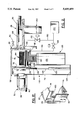
- FIG. 1 is a top plan diagrammatic view of a wafer processing system embodying the present invention, with the cover removed from the transport chamber;
- FIG. 2 is a diagrammatic side elevation view, certain parts being shown in section for clarity, illustrating in greater detail certain components illustrated in FIG. 1;
- FIG. 3 is a diagrammatic detail side elevation view, certain parts being cut away and/or shown in section for clarity, illustrating in greater detail certain components illustrated in FIG. 2 and indicating the carrier door in its closed position;
- FIG. 3A is a detail cross section view illustrating a small portion of FIG. 3;
- FIG. 4 is a diagrammatic side elevation view illustrating a portion of FIG. 2 but indicating the carrier door in its open position;
- FIG. 5 is a detail perspective view, certain parts being shown in section for clarity, illustrating in much greater detail components illustrated in FIG. 3;
- FIG. 6 is a detail side elevation view illustrating a part of FIG. 2;
- FIG. 7 is a cross section view taken generally along line 7--7 in FIG. 4;
- FIGS. 8, 9, 10, and 11 are diagrammatic side elevation views, similar to FIG. 4 but illustrating successive relative positions of the components thereof;
- FIG. 12 is a detail perspective view illustrating in much greater detail components illustrated in FIG. 2;
- FIG. 13 is a detail top plan view, largely in cross section, illustrating another embodiment of the invention.
- FIG. 14 is a further detail top plan view, in cross section, illustrating a part of FIG. 13 in greater detail and illustrating components thereof in another position;
- FIG. 15 is a detail perspective view of parts illustrated in FIG. 14, certain parts being cut away and shown in section.
- FIG. 1 illustrates a processing system 20 for operating on silicon planar substrates such as wafers and flat panels.
- wafer will be used for purposes of consistency to refer to such substrates, but it will be understood that it is intended to be used in the broad context so as to be applicable to all substrates.
- the invention is especially beneficial for operating on the newer size of substrates.
- the processing system 20 includes a load lock 22 for initially receiving wafers to be processed and a plurality of single-wafer processing stations 24 for operations on the surfaces of the wafers such as imaging, plasma etching, and the like. It is typical for the processing stations 24 to be arranged about a closed locus as indicated by a dashed line 26.
- a transport chamber 28 is disposed concentrically within the load lock 22 and processing stations 24 for singly transferring wafers to be processed and after processing between the load lock and one or more of the processing stations 24.
- a plurality of isolation valves 30 are individually provided at the interfaces of the several processing stations 24 and the transport chamber 28 and between the load lock 22 and the transport chamber 28.
- carriers transportable SMIF boxes or containers, herein referred to as "carriers" for maintaining articles, such as semiconductor wafers, clean. This has been achieved by maintaining within each carrier a substantially particle free environment while the wafers are being brought to, or removed from, the processing system 20. Previously, it was customary to carry a large number of the wafers within the carrier by supporting them in a spaced relationship by means of a cassette (not shown).
- the cassette would be loaded with a supply of wafers, transported into the carrier, then subsequently wafers would be removed from the cassette within the carrier one by one for placement in the load lock 22 or the cassette would be transferred with the wafers within the clean mini-environment existing between the carrier, SMIF box, or the like, and the wafer processing equipment.
- a modified portable carrier 32 for supporting and transporting a plurality of wafers 34 in spaced relationship in a substantially particle free environment.
- the carrier 32 has a plurality of rack member sets 36 for supporting the wafers generally horizontally, in a generally vertically spaced relationship.
- the carrier 32 includes a carrier port 38 for providing access to the interior 40 thereof.
- a carrier door 42 on the carrier is movable between a closed position (FIG. 3) overlying the carrier port and an open position (FIG. 4) spaced from the carrier port.
- the carrier door 42 is illustrated as including a generally rectangular plate 44 and has a peripherally extending continuous transverse flange 46.
- a suitable seal 48 is interposed between the flange 46 and the carrier port 38 for sealing the interior 40 of the carrier from the surrounding atmosphere when the carrier door is in the closed position.
- At least a pair of opposed locking tabs 50 extend in a direction toward the carrier 32 from the flange 46 and each locking tab has a hole 52 therethrough.
- a locking member 54 which may be in the form of a solenoid for operating a locking pin 56. Viewing especially FIG. 5, the locking member is suitably mounted on the carrier 32.
- an isolation housing or mini-environment 58 (see especially FIG. 2) is provided for sealingly isolating the load lock 22 and the interior 40 of the carrier 32 from the surrounding atmosphere.
- the carrier is brought in some suitable fashion from a remote location, then placed on a platform 60 which is a part of the mini-environment 58 and projects in a direction away from the processing system 20.
- An upper surface 62 of the platform 60 is formed with a plurality of depressions 64 properly spaced to receive feet 66 which project from the bottom of the carrier. When the feet 66 are fully engaged with the depressions 64, a front surface 68 of the carrier 32 is proximate an outer surface 70 of the mini-environment 58.
- the mini-environment has an aperture 72 which is generally aligned with the load lock 22 but spaced therefrom and when the carrier is seated on the platform 60, the carrier door 42 projects through the aperture into the interior of the mini-environment.
- a suitable seal 74 is provided between the mini-environment 58 and the carrier when supported on the platform and encompasses the carrier port 38 and the aperture 72 in the mini-environment for isolating the interior of the carrier, the interior of the mini-environment and the load lock from the surrounding atmosphere.
- a clamp actuator 304 extends or retracts an actuator rod 306 which is pivotally attached to the clamp 300 at an end distant from the part engaging the recess 302.
- the clamp actuator 304 is effective to move the clamp 300 from the solid line position engaging the recess 302 to a broken line position disengaged from the recess.
- the load lock 22 defines a chamber 76 therein having a substantially particle free environment and includes a load lock port 78 opening into the load lock chamber. As noted previously, the load lock 22 is positioned intermediate the carrier 32 and the transport chamber 28. A load lock door 80 is suitably mounted on the load lock for movement between a closed position overlying the load lock port 78 and an open position spaced therefrom.
- a load lock arm 82 within the load lock chamber 76 is movable between an inactive position distant from the carrier 32 (see FIG. 2) and an active position proximate the carrier (see FIG. 3).
- the load lock arm and its operating mechanism may be of the construction disclosed in commonly assigned and copending application Ser. No. 08/498,835 filed Jul. 6, 1995 entitled “Load Arm for Load Lock”, the disclosure of which is incorporated herein in its entirety, by reference.
- a multilevel end effector 84 is mounted on the load lock arm 82.
- the multilevel end effector 84 includes a mounting manifold 86 which is suitably mounted on and projects upwardly from the load lock arm 82 and, more specifically, from an elongated joint 88 of an articulated pair of such joints 88, 90 pivotally mounted on the load lock arm.
- a plurality of vertically spaced end effector sets 92 are integral with the mounting manifold and project outwardly from the mounting manifold in the direction of the carrier and lie in equally spaced parallel planes.
- Each end effector set 92 includes a pair of parallel laterally spaced end effector fingers 94 (see FIG. 7) which together are adapted to support a wafer in a generally horizontal plane.
- Each of the plurality of spaced end effector sets 92 is aligned with one of the rack member sets 36 when the load arm is in the active position and, therefore, with an associated wafer 34 supported in the carrier.
- the load lock door 80 and the carrier door 42 In order for movement of the multilevel end effector 84 toward and into the carrier 32 to commence in the manner about to be described, the load lock door 80 and the carrier door 42 must both be opened and moved to a remote location as seen in FIG. 8.
- the multilevel end effector 84 is then movable, when the load lock arm 82 is in the active position, from a retracted position distant from the wafers to an advanced position within the interior 40 of the carrier 32 and extending through the load lock port 78 and through the carrier port 38 for engaging and simultaneously retrieving the wafers as a grouping.
- the load lock arm 82 is operated in such a manner as to proceed to move the multilevel end effector 84 to the left (FIG. 9) with each of the end effector sets 92 advancing beneath and out of engagement with its associated wafer 34.
- the load lock arm, and with it the multilevel end effector 84 is raised a sufficient distance to lift the wafers, as a grouping, off their associated spaced rack member sets. Thereupon, while retaining that elevated positioning, the load lock arm 82 is again operated, this time in such a manner as to move the multilevel end effector 84 to the right, to the retracted position, for holding the grouping of the wafers 34 on the multilevel end effector 84 in the load lock chamber 76. See FIG. 11.
- a transport arm 96 within the transport chamber 28 may be operated for retrieving the wafers 34, one at a time, from the multilevel end effector and delivering it to a specified one of the plurality of processing stations 24.
- the carrier door drive mechanism includes a coupling device 98 which is selectively engageable with the carrier door 42 and movable between a first position (FIG. 2) remote from the carrier door and adjacent the load lock door 80 and a second position (FIG. 3) adjacent the carrier door and remote from the load lock door.
- a first actuator 100 is mounted on the carrier door and, via a drive rod 102, serves to move the coupling device 98 between the first and second positions.
- the coupling device includes a coupler frame 103 mounted on the drive rod and a pair of opposed axially aligned gripper members 104, 106 supported on and guided by the coupler frame.
- the gripper members 104, 106 include opposed axially aligned gripper rods 108 which are supported on and guided by the coupler frame 103 for movement between non-gripping positions and the gripping positions. Specifically, each gripper member 104, 106 has a transverse gripper finger 110 at its terminal end, the gripper fingers being engaged with a peripheral rim 112 of the carrier door 42 when the gripper members are in their gripping positions.
- the gripper fingers are movable between non-gripping positions (FIG. 2) free of engagement with the carrier door 42 and gripping positions (FIG. 4) in gripping engagement with the peripheral rim 112.
- Such gripping engagement of the carrier door by the gripper members 104, 106 can only occur when the coupling device 98 is in the second position.
- a second actuator 114 on the coupler frame 103 serves to move the gripper members 104, 106 between the non-gripping positions and the gripping positions via the suitably constrained gripper rods 108.
- operation of the first actuator 100 is initiated to move the coupling device 98 to the left to a location proximate the carrier door such that the gripper fingers 110 lie within the plane of the peripheral rim 112.
- operation of the second actuator 114 is initiated to move the gripping members radially until the gripping fingers firmly engage the peripheral rim 112.
- the first actuator 100 is again operated, this time to move the coupling device toward the right thereby causing an extremity 116 of the inwardly directed flange 46 to withdraw from the seal 48 which had, until now, maintained an environment isolated from the surrounding atmosphere.
- the coupling device 98 and, with it, the carrier door 42 are moved to the right to a position adjacent the load lock door 80.
- a load lock door drive mechanism 118 is then operated for moving the load lock door and, with it, the unit comprising the coupling device 98 and the carrier door 42 from the closed position to the open position.
- the load lock door 80 is held firmly against a suitable seal 120 interposed between the load lock door and the load lock 22 for isolating the load lock chamber 76 from the atmosphere (see FIGS. 2 and 12).
- This may be achieved, for example, by means of spaced, opposed, generally vertically oriented guide channels 121 integral with the load lock 22 and provided on opposite sides of the load lock door 80.
- the load lock door drive mechanism 118 includes a drive actuator 122 mounted on a base 124 of the mini-environment 58.
- the drive actuator 122 is vertically disposed with a drive actuator shaft 123 suitably attached to the load lock door 80 to move it between its raised closed position and a lowered open position remote from the region intermediate the carrier and the load lock chamber 76.
- An index drive mechanism 126 is provided for moving the load lock arm between the inactive position (FIG. 11) and the active position (FIG. 10).
- the load lock arm 82 and its operating mechanism, herein the index drive mechanism 126 may be of the construction disclosed in commonly assigned and copending application Ser. No. 08/498,835 filed Jul. 6, 1995.
- the index drive mechanism 126 includes a suitable index actuator 128 which is of the type which can advance an index actuator shaft 130, as desired, either in a macro fashion rapidly over a relatively long distance or in a micro fashion, that is, in incremental steps.
- the index actuator in one mode of operation, can move the load lock arm between an active position (FIGS. 8-10) at which all of the end effector sets 92 are aligned with their associated rack member sets 36 in the interior 40 of the carrier 42 and an inactive position (FIG. 11) at which all of the end effector sets are not so aligned with their associated rack member sets.
- a clutch 132 is engaged; in the latter instance, the clutch is disengaged.
- An arm drive mechanism 134 includes a suitable rotary actuator for moving the load lock arm 82 and, with it, the multilevel end effector 84 between the retracted and advanced positions.
- the arm drive mechanism 134 further includes engageable clutch elements 132a and 132b which only engage when the index drive mechanism moves the load lock arm and the multilevel end effector to the active position. When that occurs, the end effector 84 can be advanced into the interior of the carrier as previously described.
- a transport arm 96 within the transport chamber 28 may be operated for retrieving the wafers 34, one at a time, from the multilevel end effector and delivering it to a specified one of the plurality of processing stations 24.
- the index drive mechanism 126 may also be operated in its incremental mode to adjust the level of a particular end effector set 92 with robot end effector fingers 138 on the transport arm 96 within the transport chamber 28.
- the transport arm 96 driven by a transport actuator 140 is effective to retrieve wafers one at a time from the multilevel end effector 84 for delivery to a specified one of the processing stations 24.
- the transport arm 96 and its associated transport actuator 140 may be of the construction disclosed in commonly assigned U.S. Pat. No. 5,180,276 to Hendrickson, the disclosure of which is incorporated herein in it entirety, by reference.
- a suitable isolation valve 30, previously mentioned, is provided intermediate the load lock chamber 76 and the transport chamber 28.
- the isolation valve is sufficiently large to permit passage therethrough of the robot end effector fingers supporting a wafer 34 and is selectively operable to permit fluid intercommunication between the load lock chamber and the transport chamber in one instance and to prevent fluid intercommunication therebetween.
- failure to permit fluid intercommunication between the chambers also results in prevention of passage therethrough of the robot end effector fingers supporting a wafer 34.
- a suitable seal 142 is interposed between the load lock 22 and the transport chamber 28 for isolating the load lock and the transport chamber from the surrounding atmosphere when the isolation valve is positioned to permit fluid intercommunication between the load lock chamber and the transport chamber.
- a source of vacuum 144 is provided for selectively evacuating the load lock chamber 76 and the transport chamber 28.
- a conduit 146 extends between the source of vacuum 144 and the load lock chamber and a selectively operable valve 148 in the conduit 146 interconnects the vacuum source and the load lock chamber 76 when the load lock door 80 is closed and disconnects the vacuum source from the load lock chamber when the load lock door is open.
- a conduit 150 extends between the source of vacuum 144 and the transport chamber.
- a selectively operable valve 152 in the conduit 150 interconnects the vacuum source and the transport chamber when the transport chamber is isolated from the surrounding atmosphere.
- a carrier 162 is similar to the carrier 32 previously described for supporting and transporting a plurality of wafers 34 in spaced generally stacked relationship.
- the carrier 162 has a carrier port 164 for providing access to its interior 166.
- the carrier 162 includes a carrier door 170 which is movable between a closed position overlying the carrier port 164 for sealing the interior 166 from the surrounding atmosphere and an open position spaced from the carrier port.
- a load lock door 172 on the load lock is movable in the manner previously described between a closed position overlying the load lock port for sealing the load lock chamber from the surrounding atmosphere and an open position spaced therefrom.
- the carrier door drive mechanism and its operation are also as previously described.
- the mini-environment 168 has an aperture generally aligned with the load lock port but spaced therefrom and includes the platform 60 for supporting the carrier 162 thereon such that the carrier port 164 is proximate the aperture 174 in the mini-environment.
- a suitable seal 176 is provided between the mini-environment and the carrier when the carrier is supported on the platform and encompasses the carrier port and the aperture in the mini-environment for isolating the interior of the carrier, the interior of the mini-environment and the load lock chamber from the surrounding atmosphere.
- the carrier door drive mechanism 160 includes a coupling mechanism 178 which is selectively engageable with the carrier door 170 and movable between a first position remote from the carrier door and adjacent the load lock door and (as depicted by broken lines in FIG. 13) and a second position adjacent the carrier door and remote from the load lock door (as depicted by solid lines in FIG. 13).
- a first actuator 180 is mounted on the load lock door 172 and includes a drive rod 182 for moving the coupling mechanism 178 between the first and second positions.
- the carrier door 170 is recessed as at 184 (FIGS. 14 and 15) and has a gripper slot 186 therein.
- the coupling mechanism 178 includes a door gripper plate 188 mounted on the drive rod 182 and matingly receivable with the carrier port 164 when the coupling mechanism is in the second position as mentioned earlier.
- a door gripper bar 190 on a second actuator 192 which, in turn, is mounted on the door gripper plate 188 has a pair of bent fingers 194 at a distal end thereof movable between a gripping position grippingly engaging the gripper slot 186 in the carrier door 170 and a release position disengaged therefrom.
- a latch mechanism 196 is provided on the carrier door for selective engagement with the carrier for securely attaching the carrier door to the carrier.
- the carrier 162 has a latch recess 198 (FIG. 14) in the carrier port 164.
- the latch mechanism 196 includes a latch 200 pivotally mounted, as at 201, on the carrier door 170 for movement between a latching position engaged with the latch recess and an unlatching position disengaged from the latch recess.
- a retention pin 202 is pivotally connected to the latch at a first end 204 within the recess 184 and has a second turned end 206 opposite the first end. The turned end 206 is receivable in a slot 208 between the pair of bent fingers 194 and is engageable with the door gripper bar 190.
- a compression spring 210 encircles the retention pin 202 and is suitably supported within the recess 184 for biasing the latch 200 to the latching position.
- the spring At its left end (viewing FIGS. 14 and 15) the spring is seated against opposed shoulder members 212 which project into the recess from opposite walls of the recess 198 in the carrier door 170.
- the right end of the spring 210 bears against a c-clamp 214 fixed to the retention pin 202 an appropriate distance from the shoulder members 212.
- the retention pin and its second, turned, end 206 is biased toward the right, viewing FIGS. 13-15. In this manner, the spring 210 is effective to hold the latch 200 in a normally closed position in engagement with the latch recess 198.
- the movement of the door gripper bar 190 to move the pair of bent fingers 194 into the gripping position grippingly engaging the gripper slot 186 is effective to simultaneously move the latch to the unlatching position disengaged from the latch recess.
- the actuator 192 to hold the bent fingers 194 in engagement with the gripper slot 186 and to hold the latch 200 swung in the open position all as shown in FIG. 14
- the carrier door 170 and the door gripper plate 188 operate as a unit and can be moved by the actuator 180 to the open, broken line, position indicated in FIG. 13.
Abstract
Description
Claims (9)
Priority Applications (8)
| Application Number | Priority Date | Filing Date | Title |
|---|---|---|---|
| US08/498,597 US5609459A (en) | 1995-07-06 | 1995-07-06 | Door drive mechanisms for substrate carrier and load lock |
| TW084109347A TW278200B (en) | 1995-07-06 | 1995-09-07 | Door drive mechanisms for substrate carrier and load lock |
| PCT/US1996/011244 WO1997002199A1 (en) | 1995-07-06 | 1996-07-02 | Door drive mechanisms for substrate carrier and load lock |
| KR1019980700066A KR19990028767A (en) | 1995-07-06 | 1996-07-02 | Semiconductor Wafer Stacking System and Semiconductor Wafer Handling System |
| EP96923623A EP0886617A1 (en) | 1995-07-06 | 1996-07-02 | Door drive mechanisms for substrate carrier and load lock |
| JP50529197A JP4306798B2 (en) | 1995-07-06 | 1996-07-02 | Substrate carrier and load lock door drive device |
| AU64089/96A AU6408996A (en) | 1995-07-06 | 1996-07-02 | Door drive mechanisms for substrate carrier and load lock |
| CN96196791A CN1195332A (en) | 1995-07-06 | 1996-07-02 | Door drive mechanism for substrate carrier and load lock |
Applications Claiming Priority (1)
| Application Number | Priority Date | Filing Date | Title |
|---|---|---|---|
| US08/498,597 US5609459A (en) | 1995-07-06 | 1995-07-06 | Door drive mechanisms for substrate carrier and load lock |
Publications (1)
| Publication Number | Publication Date |
|---|---|
| US5609459A true US5609459A (en) | 1997-03-11 |
Family
ID=23981715
Family Applications (1)
| Application Number | Title | Priority Date | Filing Date |
|---|---|---|---|
| US08/498,597 Expired - Lifetime US5609459A (en) | 1995-07-06 | 1995-07-06 | Door drive mechanisms for substrate carrier and load lock |
Country Status (1)
| Country | Link |
|---|---|
| US (1) | US5609459A (en) |
Cited By (38)
| Publication number | Priority date | Publication date | Assignee | Title |
|---|---|---|---|---|
| US5741109A (en) * | 1995-07-07 | 1998-04-21 | Pri Automation, Inc. | Wafer transfer system having vertical lifting capability |
| WO1999033726A1 (en) * | 1997-12-24 | 1999-07-08 | Asyst Technologies, Inc. | Smif pod door and port door removal and return system |
| DE19813910A1 (en) * | 1998-03-28 | 1999-09-30 | Ald Vacuum Techn Gmbh | Apparatus for heat treatment of plate-shaped coated substrates |
| US6013112A (en) * | 1996-09-09 | 2000-01-11 | Tokyo Electron Limited | Relay apparatus for relaying object to be treated |
| US6074154A (en) * | 1996-08-29 | 2000-06-13 | Tokyo Electron Limited | Substrate treatment system, substrate transfer system, and substrate transfer method |
| US6079927A (en) * | 1998-04-22 | 2000-06-27 | Varian Semiconductor Equipment Associates, Inc. | Automated wafer buffer for use with wafer processing equipment |
| WO2000051920A1 (en) * | 1999-03-03 | 2000-09-08 | Pri Automation, Inc. | Robot to remove a substrate carrier door |
| US6120229A (en) * | 1999-02-01 | 2000-09-19 | Brooks Automation Inc. | Substrate carrier as batchloader |
| US6142722A (en) * | 1998-06-17 | 2000-11-07 | Genmark Automation, Inc. | Automated opening and closing of ultra clean storage containers |
| US6168364B1 (en) * | 1999-04-19 | 2001-01-02 | Tdk Corporation | Vacuum clean box, clean transfer method and apparatus therefor |
| US6224679B1 (en) | 1997-08-12 | 2001-05-01 | Tokyo Electron Limited | Controlling gas in a multichamber processing system |
| US6347919B1 (en) | 1999-12-17 | 2002-02-19 | Eaton Corporation | Wafer processing chamber having separable upper and lower halves |
| US6429139B1 (en) | 1999-12-17 | 2002-08-06 | Eaton Corporation | Serial wafer handling mechanism |
| US20020137346A1 (en) * | 2001-03-12 | 2002-09-26 | Applied Materials. Inc. | Workpiece distribution and processing in a high throughput stacked frame |
| US6473996B1 (en) * | 1999-11-25 | 2002-11-05 | Semiconductor Leading Edge Technologies, Inc. | Load port system for substrate processing system, and method of processing substrate |
| US6481945B1 (en) * | 1998-06-05 | 2002-11-19 | Asm International N.V. | Method and device for transferring wafers |
| US6533521B1 (en) | 2001-03-29 | 2003-03-18 | Genmark Automation, Inc. | Integrated substrate handler having pre-aligner and storage pod access mechanism |
| DE10144955A1 (en) * | 2001-09-12 | 2003-03-27 | Asys Gmbh | Arrangement for supplying microsystems has transport container with removable lid for connection to transition station lock gate and for movement with gate to open position |
| US6561894B1 (en) | 1999-04-19 | 2003-05-13 | Tdk Corporation | Clean box, clean transfer method and apparatus therefor |
| US20030152445A1 (en) * | 2002-02-08 | 2003-08-14 | Takayuki Yamagishi | Semiconductor processing apparatus comprising chamber partitioned into reaction and transfer sections |
| US6641350B2 (en) * | 2000-04-17 | 2003-11-04 | Hitachi Kokusai Electric Inc. | Dual loading port semiconductor processing equipment |
| US6676356B2 (en) * | 2000-09-18 | 2004-01-13 | Tokyo Electron Limited | Device for attaching target substrate transfer container to semiconductor processing apparatus |
| US6685422B2 (en) | 1999-03-18 | 2004-02-03 | Applied Materials Inc. | Pneumatically actuated flexure gripper for wafer handling robots |
| US20040047714A1 (en) * | 2002-09-06 | 2004-03-11 | Recif, Societe Anonyme | System for the conveying and storage of containers of semiconductor wafers, and transfer mechanism |
| US20050265812A1 (en) * | 2004-05-28 | 2005-12-01 | Tdk Corporation | Load port for clean system |
| US7018504B1 (en) | 2000-09-11 | 2006-03-28 | Asm America, Inc. | Loadlock with integrated pre-clean chamber |
| DE102004058108A1 (en) * | 2004-12-01 | 2006-06-08 | Asys Automatic Systems Gmbh & Co. Kg | Transfer device for microsystem `s laminar substrate in processing system, has transfer mechanism with articular arm whose end part carries adjustable temporary storage as hand or gripper part, where storage is integral part of mechanism |
| US20080202416A1 (en) * | 2006-01-19 | 2008-08-28 | Provencher Timothy J | High temperature ALD inlet manifold |
| US20100190343A1 (en) * | 2009-01-28 | 2010-07-29 | Asm America, Inc. | Load lock having secondary isolation chamber |
| DE102013016598A1 (en) | 2013-10-08 | 2015-04-09 | Asys Automatic Systems Gmbh & Co. Kg | Clean room transport container with chassis |
| DE102013016597A1 (en) | 2013-10-08 | 2015-04-09 | Asys Automatic Systems Gmbh & Co. Kg | System for loading and unloading clean room systems with large-area substrates |
| US20150276471A1 (en) * | 2014-03-28 | 2015-10-01 | Mettler-Toledo Ag | Robot-actuated door-opening device for a draft shield enclosure of an analytical balance |
| DE102014008340A1 (en) * | 2014-06-12 | 2015-12-17 | Asys Automatic Systems Gmbh & Co. Kg | Loading / unloading unit for clean room systems |
| US9388492B2 (en) | 2011-12-27 | 2016-07-12 | Asm America, Inc. | Vapor flow control apparatus for atomic layer deposition |
| US9574268B1 (en) | 2011-10-28 | 2017-02-21 | Asm America, Inc. | Pulsed valve manifold for atomic layer deposition |
| US10662527B2 (en) | 2016-06-01 | 2020-05-26 | Asm Ip Holding B.V. | Manifolds for uniform vapor deposition |
| US11492701B2 (en) | 2019-03-19 | 2022-11-08 | Asm Ip Holding B.V. | Reactor manifolds |
| US11830731B2 (en) | 2019-10-22 | 2023-11-28 | Asm Ip Holding B.V. | Semiconductor deposition reactor manifolds |
Citations (29)
| Publication number | Priority date | Publication date | Assignee | Title |
|---|---|---|---|---|
| US4381965A (en) * | 1982-01-06 | 1983-05-03 | Drytek, Inc. | Multi-planar electrode plasma etching |
| US4550242A (en) * | 1981-10-05 | 1985-10-29 | Tokyo Denshi Kagaku Kabushiki Kaisha | Automatic plasma processing device and heat treatment device for batch treatment of workpieces |
| US4674939A (en) * | 1984-07-30 | 1987-06-23 | Asyst Technologies | Sealed standard interface apparatus |
| US4674936A (en) * | 1985-08-26 | 1987-06-23 | Asyst Technologies | Short arm manipulator for standard mechanical interface apparatus |
| US4676709A (en) * | 1985-08-26 | 1987-06-30 | Asyst Technologies | Long arm manipulator for standard mechanical interface apparatus |
| JPS62252128A (en) * | 1986-04-25 | 1987-11-02 | Hitachi Ltd | Substrate introducing device for semiconductor manufacturing apparatus |
| WO1987007309A1 (en) * | 1986-05-19 | 1987-12-03 | Novellus Systems, Inc. | Deposition apparatus with automatic cleaning means and method of use |
| US4715921A (en) * | 1986-10-24 | 1987-12-29 | General Signal Corporation | Quad processor |
| US4724874A (en) * | 1986-05-01 | 1988-02-16 | Asyst Technologies | Sealable transportable container having a particle filtering system |
| US4730976A (en) * | 1983-02-14 | 1988-03-15 | Aeronca Electronics, Inc. | Articulated arm transfer device |
| US4739882A (en) * | 1986-02-13 | 1988-04-26 | Asyst Technologies | Container having disposable liners |
| US4789294A (en) * | 1985-08-30 | 1988-12-06 | Canon Kabushiki Kaisha | Wafer handling apparatus and method |
| US4815912A (en) * | 1984-12-24 | 1989-03-28 | Asyst Technologies, Inc. | Box door actuated retainer |
| US4951601A (en) * | 1986-12-19 | 1990-08-28 | Applied Materials, Inc. | Multi-chamber integrated process system |
| US4995430A (en) * | 1989-05-19 | 1991-02-26 | Asyst Technologies, Inc. | Sealable transportable container having improved latch mechanism |
| JPH0461146A (en) * | 1990-06-22 | 1992-02-27 | Mitsubishi Electric Corp | Shifter for semiconductor wafer |
| JPH04106952A (en) * | 1990-08-27 | 1992-04-08 | Kokusai Electric Co Ltd | Apparatus for hold-transferring wafer |
| US5110248A (en) * | 1989-07-17 | 1992-05-05 | Tokyo Electron Sagami Limited | Vertical heat-treatment apparatus having a wafer transfer mechanism |
| JPH04206547A (en) * | 1990-11-30 | 1992-07-28 | Hitachi Ltd | Interdevice transfer method |
| US5133284A (en) * | 1990-07-16 | 1992-07-28 | National Semiconductor Corp. | Gas-based backside protection during substrate processing |
| US5166884A (en) * | 1984-12-24 | 1992-11-24 | Asyst Technologies, Inc. | Intelligent system for processing and storing articles |
| US5169272A (en) * | 1990-11-01 | 1992-12-08 | Asyst Technologies, Inc. | Method and apparatus for transferring articles between two controlled environments |
| US5180276A (en) * | 1991-04-18 | 1993-01-19 | Brooks Automation, Inc. | Articulated arm transfer device |
| US5183370A (en) * | 1989-12-29 | 1993-02-02 | Commissariat A L'energie Atomique | Apparatus for placing or storing flat articles in a cassette with intermediate racks |
| JPH0672508A (en) * | 1992-08-28 | 1994-03-15 | Kiyoshi Takahashi | Wafer replacing device |
| US5382128A (en) * | 1993-03-03 | 1995-01-17 | Takahashi; Kiyoshi | Wafer transfer device |
| US5395198A (en) * | 1992-06-19 | 1995-03-07 | International Business Machines Corporation | Vacuum loading chuck and fixture for flexible printed circuit panels |
| US5404894A (en) * | 1992-05-20 | 1995-04-11 | Tokyo Electron Kabushiki Kaisha | Conveyor apparatus |
| US5431600A (en) * | 1992-10-06 | 1995-07-11 | Shinko Electric Co., Ltd. | Automatic transferring system using portable closed container |
-
1995
- 1995-07-06 US US08/498,597 patent/US5609459A/en not_active Expired - Lifetime
Patent Citations (30)
| Publication number | Priority date | Publication date | Assignee | Title |
|---|---|---|---|---|
| US4550242A (en) * | 1981-10-05 | 1985-10-29 | Tokyo Denshi Kagaku Kabushiki Kaisha | Automatic plasma processing device and heat treatment device for batch treatment of workpieces |
| US4381965A (en) * | 1982-01-06 | 1983-05-03 | Drytek, Inc. | Multi-planar electrode plasma etching |
| US4730976A (en) * | 1983-02-14 | 1988-03-15 | Aeronca Electronics, Inc. | Articulated arm transfer device |
| US4674939A (en) * | 1984-07-30 | 1987-06-23 | Asyst Technologies | Sealed standard interface apparatus |
| US5166884A (en) * | 1984-12-24 | 1992-11-24 | Asyst Technologies, Inc. | Intelligent system for processing and storing articles |
| US4815912A (en) * | 1984-12-24 | 1989-03-28 | Asyst Technologies, Inc. | Box door actuated retainer |
| US4674936A (en) * | 1985-08-26 | 1987-06-23 | Asyst Technologies | Short arm manipulator for standard mechanical interface apparatus |
| US4802809A (en) * | 1985-08-26 | 1989-02-07 | Asyst Technologies | Manipulator for standard mechanical interface apparatus |
| US4676709A (en) * | 1985-08-26 | 1987-06-30 | Asyst Technologies | Long arm manipulator for standard mechanical interface apparatus |
| US4789294A (en) * | 1985-08-30 | 1988-12-06 | Canon Kabushiki Kaisha | Wafer handling apparatus and method |
| US4739882A (en) * | 1986-02-13 | 1988-04-26 | Asyst Technologies | Container having disposable liners |
| JPS62252128A (en) * | 1986-04-25 | 1987-11-02 | Hitachi Ltd | Substrate introducing device for semiconductor manufacturing apparatus |
| US4724874A (en) * | 1986-05-01 | 1988-02-16 | Asyst Technologies | Sealable transportable container having a particle filtering system |
| WO1987007309A1 (en) * | 1986-05-19 | 1987-12-03 | Novellus Systems, Inc. | Deposition apparatus with automatic cleaning means and method of use |
| US4715921A (en) * | 1986-10-24 | 1987-12-29 | General Signal Corporation | Quad processor |
| US4951601A (en) * | 1986-12-19 | 1990-08-28 | Applied Materials, Inc. | Multi-chamber integrated process system |
| US4995430A (en) * | 1989-05-19 | 1991-02-26 | Asyst Technologies, Inc. | Sealable transportable container having improved latch mechanism |
| US5110248A (en) * | 1989-07-17 | 1992-05-05 | Tokyo Electron Sagami Limited | Vertical heat-treatment apparatus having a wafer transfer mechanism |
| US5183370A (en) * | 1989-12-29 | 1993-02-02 | Commissariat A L'energie Atomique | Apparatus for placing or storing flat articles in a cassette with intermediate racks |
| JPH0461146A (en) * | 1990-06-22 | 1992-02-27 | Mitsubishi Electric Corp | Shifter for semiconductor wafer |
| US5133284A (en) * | 1990-07-16 | 1992-07-28 | National Semiconductor Corp. | Gas-based backside protection during substrate processing |
| JPH04106952A (en) * | 1990-08-27 | 1992-04-08 | Kokusai Electric Co Ltd | Apparatus for hold-transferring wafer |
| US5169272A (en) * | 1990-11-01 | 1992-12-08 | Asyst Technologies, Inc. | Method and apparatus for transferring articles between two controlled environments |
| JPH04206547A (en) * | 1990-11-30 | 1992-07-28 | Hitachi Ltd | Interdevice transfer method |
| US5180276A (en) * | 1991-04-18 | 1993-01-19 | Brooks Automation, Inc. | Articulated arm transfer device |
| US5404894A (en) * | 1992-05-20 | 1995-04-11 | Tokyo Electron Kabushiki Kaisha | Conveyor apparatus |
| US5395198A (en) * | 1992-06-19 | 1995-03-07 | International Business Machines Corporation | Vacuum loading chuck and fixture for flexible printed circuit panels |
| JPH0672508A (en) * | 1992-08-28 | 1994-03-15 | Kiyoshi Takahashi | Wafer replacing device |
| US5431600A (en) * | 1992-10-06 | 1995-07-11 | Shinko Electric Co., Ltd. | Automatic transferring system using portable closed container |
| US5382128A (en) * | 1993-03-03 | 1995-01-17 | Takahashi; Kiyoshi | Wafer transfer device |
Cited By (61)
| Publication number | Priority date | Publication date | Assignee | Title |
|---|---|---|---|---|
| US5741109A (en) * | 1995-07-07 | 1998-04-21 | Pri Automation, Inc. | Wafer transfer system having vertical lifting capability |
| US6074154A (en) * | 1996-08-29 | 2000-06-13 | Tokyo Electron Limited | Substrate treatment system, substrate transfer system, and substrate transfer method |
| US6655891B2 (en) * | 1996-08-29 | 2003-12-02 | Tokyo Electron Limited | Substrate treatment system, substrate transfer system, and substrate transfer method |
| US6425722B1 (en) * | 1996-08-29 | 2002-07-30 | Tokyo Electron Limited | Substrate treatment system, substrate transfer system, and substrate transfer method |
| US6013112A (en) * | 1996-09-09 | 2000-01-11 | Tokyo Electron Limited | Relay apparatus for relaying object to be treated |
| US6224679B1 (en) | 1997-08-12 | 2001-05-01 | Tokyo Electron Limited | Controlling gas in a multichamber processing system |
| WO1999033726A1 (en) * | 1997-12-24 | 1999-07-08 | Asyst Technologies, Inc. | Smif pod door and port door removal and return system |
| US6704998B1 (en) | 1997-12-24 | 2004-03-16 | Asyst Technologies, Inc. | Port door removal and wafer handling robotic system |
| DE19813910A1 (en) * | 1998-03-28 | 1999-09-30 | Ald Vacuum Techn Gmbh | Apparatus for heat treatment of plate-shaped coated substrates |
| US6079927A (en) * | 1998-04-22 | 2000-06-27 | Varian Semiconductor Equipment Associates, Inc. | Automated wafer buffer for use with wafer processing equipment |
| US6481945B1 (en) * | 1998-06-05 | 2002-11-19 | Asm International N.V. | Method and device for transferring wafers |
| US6142722A (en) * | 1998-06-17 | 2000-11-07 | Genmark Automation, Inc. | Automated opening and closing of ultra clean storage containers |
| US6120229A (en) * | 1999-02-01 | 2000-09-19 | Brooks Automation Inc. | Substrate carrier as batchloader |
| US6520726B1 (en) | 1999-03-03 | 2003-02-18 | Pri Automation, Inc. | Apparatus and method for using a robot to remove a substrate carrier door |
| WO2000051920A1 (en) * | 1999-03-03 | 2000-09-08 | Pri Automation, Inc. | Robot to remove a substrate carrier door |
| US6685422B2 (en) | 1999-03-18 | 2004-02-03 | Applied Materials Inc. | Pneumatically actuated flexure gripper for wafer handling robots |
| US6168364B1 (en) * | 1999-04-19 | 2001-01-02 | Tdk Corporation | Vacuum clean box, clean transfer method and apparatus therefor |
| US6561894B1 (en) | 1999-04-19 | 2003-05-13 | Tdk Corporation | Clean box, clean transfer method and apparatus therefor |
| US6473996B1 (en) * | 1999-11-25 | 2002-11-05 | Semiconductor Leading Edge Technologies, Inc. | Load port system for substrate processing system, and method of processing substrate |
| US6347919B1 (en) | 1999-12-17 | 2002-02-19 | Eaton Corporation | Wafer processing chamber having separable upper and lower halves |
| US6429139B1 (en) | 1999-12-17 | 2002-08-06 | Eaton Corporation | Serial wafer handling mechanism |
| KR100573833B1 (en) * | 1999-12-17 | 2006-04-26 | 액셀리스 테크놀로지스, 인크. | Wafer processing chamber having separable upper and lower halves |
| USRE43023E1 (en) | 2000-04-17 | 2011-12-13 | Hitachi Kokusai Electric Inc. | Dual loading port semiconductor processing equipment |
| US6641350B2 (en) * | 2000-04-17 | 2003-11-04 | Hitachi Kokusai Electric Inc. | Dual loading port semiconductor processing equipment |
| US7018504B1 (en) | 2000-09-11 | 2006-03-28 | Asm America, Inc. | Loadlock with integrated pre-clean chamber |
| US6676356B2 (en) * | 2000-09-18 | 2004-01-13 | Tokyo Electron Limited | Device for attaching target substrate transfer container to semiconductor processing apparatus |
| US20020137346A1 (en) * | 2001-03-12 | 2002-09-26 | Applied Materials. Inc. | Workpiece distribution and processing in a high throughput stacked frame |
| US6533521B1 (en) | 2001-03-29 | 2003-03-18 | Genmark Automation, Inc. | Integrated substrate handler having pre-aligner and storage pod access mechanism |
| DE10144955B4 (en) * | 2001-09-12 | 2006-06-29 | Asys Automatic Systems Gmbh & Co. Kg | Device for feeding microsystems |
| DE10144955A1 (en) * | 2001-09-12 | 2003-03-27 | Asys Gmbh | Arrangement for supplying microsystems has transport container with removable lid for connection to transition station lock gate and for movement with gate to open position |
| US20050118001A1 (en) * | 2002-02-08 | 2005-06-02 | Takayuki Yamagishi | Semiconductor processing apparatus comprising chamber partitioned into reaction and transfer sections |
| US20030152445A1 (en) * | 2002-02-08 | 2003-08-14 | Takayuki Yamagishi | Semiconductor processing apparatus comprising chamber partitioned into reaction and transfer sections |
| US7021881B2 (en) | 2002-02-08 | 2006-04-04 | Asm Japan K.K. | Semiconductor processing apparatus comprising chamber partitioned into reaction and transfer sections |
| US6899507B2 (en) | 2002-02-08 | 2005-05-31 | Asm Japan K.K. | Semiconductor processing apparatus comprising chamber partitioned into reaction and transfer sections |
| US20040047714A1 (en) * | 2002-09-06 | 2004-03-11 | Recif, Societe Anonyme | System for the conveying and storage of containers of semiconductor wafers, and transfer mechanism |
| US20050265812A1 (en) * | 2004-05-28 | 2005-12-01 | Tdk Corporation | Load port for clean system |
| DE102004058108A1 (en) * | 2004-12-01 | 2006-06-08 | Asys Automatic Systems Gmbh & Co. Kg | Transfer device for microsystem `s laminar substrate in processing system, has transfer mechanism with articular arm whose end part carries adjustable temporary storage as hand or gripper part, where storage is integral part of mechanism |
| DE102004058108B4 (en) * | 2004-12-01 | 2006-12-28 | Asys Automatic Systems Gmbh & Co. Kg | Transfer unit of a processing plant |
| US20080202416A1 (en) * | 2006-01-19 | 2008-08-28 | Provencher Timothy J | High temperature ALD inlet manifold |
| US7918938B2 (en) | 2006-01-19 | 2011-04-05 | Asm America, Inc. | High temperature ALD inlet manifold |
| US20110162580A1 (en) * | 2006-01-19 | 2011-07-07 | Asm America, Inc. | High temperature ald inlet manifold |
| US8372201B2 (en) | 2006-01-19 | 2013-02-12 | Asm America, Inc. | High temperature ALD inlet manifold |
| US20100190343A1 (en) * | 2009-01-28 | 2010-07-29 | Asm America, Inc. | Load lock having secondary isolation chamber |
| US8440048B2 (en) | 2009-01-28 | 2013-05-14 | Asm America, Inc. | Load lock having secondary isolation chamber |
| US8927435B2 (en) | 2009-01-28 | 2015-01-06 | Asm America, Inc. | Load lock having secondary isolation chamber |
| US20170121818A1 (en) | 2011-10-28 | 2017-05-04 | Asm America, Inc. | Pulsed valve manifold for atomic layer deposition |
| US9574268B1 (en) | 2011-10-28 | 2017-02-21 | Asm America, Inc. | Pulsed valve manifold for atomic layer deposition |
| US10370761B2 (en) | 2011-10-28 | 2019-08-06 | Asm America, Inc. | Pulsed valve manifold for atomic layer deposition |
| US11208722B2 (en) | 2011-12-27 | 2021-12-28 | Asm Ip Holding B.V. | Vapor flow control apparatus for atomic layer deposition |
| US9388492B2 (en) | 2011-12-27 | 2016-07-12 | Asm America, Inc. | Vapor flow control apparatus for atomic layer deposition |
| DE102013016598A1 (en) | 2013-10-08 | 2015-04-09 | Asys Automatic Systems Gmbh & Co. Kg | Clean room transport container with chassis |
| DE102013016597A1 (en) | 2013-10-08 | 2015-04-09 | Asys Automatic Systems Gmbh & Co. Kg | System for loading and unloading clean room systems with large-area substrates |
| DE102013016598B4 (en) * | 2013-10-08 | 2021-06-10 | Asys Automatic Systems Gmbh & Co. Kg | Clean room transport container with chassis |
| US9574932B2 (en) * | 2014-03-28 | 2017-02-21 | Mettler-Toledo Gmbh | Robot-actuated door-opening device for a draft shield enclosure of an analytical balance |
| US20150276471A1 (en) * | 2014-03-28 | 2015-10-01 | Mettler-Toledo Ag | Robot-actuated door-opening device for a draft shield enclosure of an analytical balance |
| DE102014008340B4 (en) * | 2014-06-12 | 2017-10-19 | Asys Automatic Systems Gmbh & Co. Kg | Cluster of a clean room facility |
| DE102014008340A1 (en) * | 2014-06-12 | 2015-12-17 | Asys Automatic Systems Gmbh & Co. Kg | Loading / unloading unit for clean room systems |
| US10662527B2 (en) | 2016-06-01 | 2020-05-26 | Asm Ip Holding B.V. | Manifolds for uniform vapor deposition |
| US11377737B2 (en) | 2016-06-01 | 2022-07-05 | Asm Ip Holding B.V. | Manifolds for uniform vapor deposition |
| US11492701B2 (en) | 2019-03-19 | 2022-11-08 | Asm Ip Holding B.V. | Reactor manifolds |
| US11830731B2 (en) | 2019-10-22 | 2023-11-28 | Asm Ip Holding B.V. | Semiconductor deposition reactor manifolds |
Similar Documents
| Publication | Publication Date | Title |
|---|---|---|
| US5609459A (en) | Door drive mechanisms for substrate carrier and load lock | |
| US5613821A (en) | Cluster tool batchloader of substrate carrier | |
| US5664925A (en) | Batchloader for load lock | |
| US5607276A (en) | Batchloader for substrate carrier on load lock | |
| US6120229A (en) | Substrate carrier as batchloader | |
| US5752796A (en) | Vacuum integrated SMIF system | |
| KR100639765B1 (en) | Method and apparatus for processing substrates and semiconductor device manufacturing method | |
| US4859137A (en) | Apparatus for transporting a holder between a port opening of a standardized mechanical interface system and a loading and unloading station | |
| US6517304B1 (en) | Method for transporting substrates and a semiconductor manufacturing apparatus using the method | |
| EP0980585B1 (en) | Multiple single-wafer loadlock wafer processing apparatus and loading and unloading method therefor | |
| US6176023B1 (en) | Device for transporting flat objects and process for transferring said objects between said device and a processing machine | |
| US6042623A (en) | Two-wafer loadlock wafer processing apparatus and loading and unloading method therefor | |
| JP3417821B2 (en) | Clean box, clean transfer method and device | |
| EP0191805B1 (en) | Sealed standard interface apparatus | |
| TWI823166B (en) | Load port operation in electronic device manufacturing apparatus, systems, and methods | |
| JP4306798B2 (en) | Substrate carrier and load lock door drive device | |
| EP1084509A1 (en) | Batch end effector for semiconductor wafer handling | |
| JP2022551815A (en) | Substrate processing equipment | |
| KR20020071467A (en) | Substrate processing apparatus | |
| KR20030065275A (en) | Substrate container with non-friction door element | |
| KR100292065B1 (en) | Standard mechanical interface system having function for eliminating contamination particle | |
| JPWO2020252476A5 (en) | ||
| JPH0385723A (en) | Longitudinal cvd device |
Legal Events
| Date | Code | Title | Description |
|---|---|---|---|
| AS | Assignment |
Owner name: BROOKS AUTOMATION, INC., MASSACHUSETTS Free format text: ASSIGNMENT OF ASSIGNORS INTEREST;ASSIGNOR:MUKA, RICHARD S.;REEL/FRAME:007668/0576 Effective date: 19950901 |
|
| STCF | Information on status: patent grant |
Free format text: PATENTED CASE |
|
| FPAY | Fee payment |
Year of fee payment: 4 |
|
| FEPP | Fee payment procedure |
Free format text: PAYOR NUMBER ASSIGNED (ORIGINAL EVENT CODE: ASPN); ENTITY STATUS OF PATENT OWNER: LARGE ENTITY |
|
| FPAY | Fee payment |
Year of fee payment: 8 |
|
| REMI | Maintenance fee reminder mailed | ||
| FPAY | Fee payment |
Year of fee payment: 12 |
|
| SULP | Surcharge for late payment |
Year of fee payment: 11 |
|
| FEPP | Fee payment procedure |
Free format text: PAYER NUMBER DE-ASSIGNED (ORIGINAL EVENT CODE: RMPN); ENTITY STATUS OF PATENT OWNER: LARGE ENTITY Free format text: PAYOR NUMBER ASSIGNED (ORIGINAL EVENT CODE: ASPN); ENTITY STATUS OF PATENT OWNER: LARGE ENTITY |
|
| AS | Assignment |
Owner name: MORGAN STANLEY SENIOR FUNDING, INC., MARYLAND Free format text: SECURITY INTEREST;ASSIGNORS:BROOKS AUTOMATION, INC.;BIOSTORAGE TECHNOLOGIES, INC.;REEL/FRAME:044142/0258 Effective date: 20171004 |