US5585797A - Signal processing device having a function of converting an analog signal into a digital signal - Google Patents
Signal processing device having a function of converting an analog signal into a digital signal Download PDFInfo
- Publication number
- US5585797A US5585797A US08/240,465 US24046594A US5585797A US 5585797 A US5585797 A US 5585797A US 24046594 A US24046594 A US 24046594A US 5585797 A US5585797 A US 5585797A
- Authority
- US
- United States
- Prior art keywords
- signal
- voltage
- output
- electric charge
- transfer
- Prior art date
- Legal status (The legal status is an assumption and is not a legal conclusion. Google has not performed a legal analysis and makes no representation as to the accuracy of the status listed.)
- Expired - Lifetime
Links
Images


Classifications
-
- H—ELECTRICITY
- H03—ELECTRONIC CIRCUITRY
- H03M—CODING; DECODING; CODE CONVERSION IN GENERAL
- H03M1/00—Analogue/digital conversion; Digital/analogue conversion
- H03M1/12—Analogue/digital converters
- H03M1/50—Analogue/digital converters with intermediate conversion to time interval
Definitions
- the present invention relates to a signal processing device, and more specifically to a signal processing device for converting into a digital signal a signal charge amount outputted from an electric charge transfer device typified particularly by a charge transfer device type image sensor and a charge transfer device type delay line.
- an analog signal outputted from a charge transfer device type image sensor or a charge transfer device type delay line for example, as shown in FIG. 1, an analog signal outputted from a charge transfer device type image sensor 61 is caused to pass through a buffer 66, a clamp circuit 67, a sample-hold circuit 68, a low pass filter 69, and an amplifier 70 for various signal processings, and thereafter, the analog signal is supplied an A/D converter (analog-to-digital converter) 71, so that a digital signal is obtained.
- A/D converter analog-to-digital converter
- the charge transfer device type image sensor 61 is basically composed of a number of photosensor cells such as photodiodes 62 arranged in the form of a matrix having a plurality of rows and a plurality of columns, a plurality of vertical charge transfer devices each located along a corresponding column of photodiodes so as to receive an electric charge from all the photodiodes of the corresponding column in parallel and to vertically transfer the received electric charges, a horizontal charge transfer device located along an output end of all the vertical charge transfer devices so as to receive an electric charge from all the vertical charge transfer devices in parallel and to horizontally transfer the received electric charge, and an electric charge detection circuit 65 having an input coupled to an output end of the horizontal charge transfer device. An output of the electric charge detection circuit 65 is connected to the buffer 66.
- JP-A-61-184978 has proposed a signal processing device which attempts to improve the above mentioned problems and includes a charge coupled device (abbreviated "CCD” hereinafter) as the charge transfer device
- CCD charge coupled device
- the proposed signal processing device includes two two-bit A/D converters so that one of the two-bit A/D converters is used for the more significant two bits, and the other two-bit A/D converter is used for the least significant two bits, whereby a resolution of 4 bits per sample can be obtained in total.
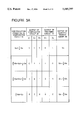
- FIG. 2 there is shown a block diagram illustrating the construction of the A/D converter disclosed in the above referred Japanese patent application laid-open publication.
- FIGS. 3A and 3B are tables illustrating an operation of the shown A/D converter.
- the shown A/D converter includes a tapped CCD delay line 31, which is coupled to an output of a CCD image sensor or delay line so as to receive a signal electric charge transferred in a transfer direction 32.
- the signal electric charge is transferred through the tapped CCD delay line 31.
- the magnitude of the signal electric charge is nondestructively detected, so that a signal voltage is applied from signal electric charge output terminals 33, 34 and 35 to a signal input terminal of analog comparators 39, 38 and 37 included in an analog comparator group 36.
- a reference voltage is V R
- a reference voltage terminal of these analog comparators 37, 38 and 39 are supplied with 3V R /4, V R /2, and V R /4, respectively, which are generated in a reference voltage generation circuit 40.
- the discrimination signals C 1 , C 2 and C 3 outputted from the analog comparators 37, 38 and 39, are respectively supplied to digital shift registers 41, 42 and 43 having different delay times for compensating the fact that the detection for the same signal charge is delayed one clock by one clock from the terminal 33 to the terminal 34 and also from the terminal 34 to the terminal 35, as would be apparent from the operation of the tapped charge transfer device delay line 31.
- the digital shift registers 41, 42 and 43 are driven by a clock having the same frequency as that of a clock for driving the tapped charge transfer device delay line 31, and the delay times of the digital shift registers 41, 42 and 43 are selected to correspond to the delay time occurring in the tapped charge transfer device delay line 31.
- the discrimination signals C 1 , C 2 and C 3 thus adjusted to have concurrency by action of the digital shift registers 41, 42 and 43, are supplied to an encoder 44, where the discrimination signals C 1 , C 2 and C 3 are converted to binary signals D 1 and D 2 of two bits as shown in FIG. 3A.
- the A/D conversion for obtaining two most significant bits can be realized.
- the discrimination signals C 1 , C 2 and C 3 are applied to a bias electric charge generator 45, which is configured to generate and add a bias electric charge corresponding to V R /4 for each of the discrimination signals C 1 , C 2 and C 3 when the discrimination signal is at the low level "0". Namely, as shown in FIG. 3B, when all of the discrimination signals C 1 , C 2 and C 3 are at the high level "1", no bias electric charge is generated and added. When only the discrimination signal C 1 is at the low level "0", a bias electric charge corresponding to V R /4 is generated, and added to the electric charge outputted from the tapped charge transfer device delay line 31, in a bias electric charge adder 46.
- both of the discrimination signals C 1 and C 2 are at the low level "0"
- a bias electric charge corresponding to V R /2 is generated and added in the bias electric charge adder 46.
- a bias electric charge corresponding to 3V R /4 is generated and added in the bias electric charge adder 46.
- the signal electric thus added with the bias electric charge is supplied from the bias electric charge adder 46 to another tapped charge transfer device delay line 47 so as to be transferred through the tapped charge transfer device delay line 47.
- the electric charge through the tapped charge transfer device delay line 47 is nondestructively detected at each one of the stage transfer operation, so that a synthetic signal voltage is applied from signal electric charge output terminals 48, 49 and 50 to a signal input terminal of analog comparators 54, 53 and 52 included in another analog comparator group 51.
- a reference voltage terminal of these analog comparators 52, 53 and 54 are supplied with 15V R /16, 14V R /16, and 13V R /16, respectively, which are generated in a reference voltage generation circuit 55.
- the discriminating condition for the signal voltage V s can be sorted into 16 kinds as shown in FIG. 3B.
- the discrimination signals C 4 , C 5 and C 6 outputted from the analog comparators 52, 53 and 54, are respectively supplied to digital shift registers 56, 57 and 57 having different delay times for compensating differences in the delay time.
- the discrimination signals C 4 , C 5 and C 6 thus adjusted to have concurrency by action of the digital shift registers 56, 57 and 57, are supplied to an encoder 59, in which the discrimination signals C 4 , C 5 and C 6 are converted to binary signals D 3 and D 4 of two bits as shown in FIG. 3B.
- an A/D conversion section for obtaining two least significant bits can be constituted of the tapped charge transfer device delay line 47, the analog comparator group 51, the reference voltage generation circuit 55, the digital shift registers 56, 57 and 58, the encoder 59.
- an A/D converter having a resolution of 4 bits per sample can be acheived.
- the above mentioned signal processing device for converting the analog signal to the digital signal had to include a number of nondestructive electric charge detection circuits and reference voltages in correspondence to the number of the electric charge amounts to be detected.
- the four-bit A/D converter there are required six analog comparators, six digital shift registers, and six charge transfer delay line stages.
- the digital output signals are synchronized to have concurrency in time by the digital shift registers, the circuit construction inevitably becomes complicated.
- Another object of the present invention is to provide a circuit which can give a digital signal corresponding to a signal electric charge, and which is remarkably simpler than the conventional circuit.
- a signal processing device comprising:
- a charge transfer device including a charge transfer section composed of a plurality of transfer electrodes formed through a gate insulating film on a surface of a semiconductor substrate and arranged in the form of a column, a final transfer gate located adjacent to an output end of the charge transfer section, an output gate located adjacent to the final transfer gate, and an electric charge detection means located adjacent to the output gate; and
- a driving circuit including a reference signal generating circuit for generating a reference signal, a transfer clock generating circuit receiving the reference signal for generating a transfer clock to the charge transfer section, a digital counter of N bits receiving and counting the reference signal, a voltage generating means for generating a voltage starting to change in synchronism with the start of a counting operation of the counter, the voltage being applied to one of the final transfer gate and the output gate, and a latch for latching an output of the counter when an output of the electric charge detection means reaches a predetermined level,
- the latch outputs a digital signal of N bits corresponding to a signal electric charge outputted from the charge transfer section.
- the voltage generating means includes a D/A converter receiving the output of the counter for converting, it into an analog voltage signal, which is applied to the final transfer gate.
- the voltage generating means includes a saw tooth wave generating circuit for generating a saw tooth wave in response to an output signal of the transfer clock generating circuit and in synchronism with the reference signal, the saw tooth wave being applied to the final transfer gate.
- the transfer clock is also applied to the final transfer gate
- the voltage generating means includes a saw tooth wave generating circuit for generating a saw tooth wave in response to an output signal of the transfer clock generating circuit and in synchronism with the reference signal, the saw tooth wave being applied to the output gate.
- the electric charge detection means can be of a voltage detection type.
- the circuit further includes a voltage comparator having an inverted input connected to receive an output signal of the electric charge detection means and a non-inverted input connected to a reference voltage, an output of the voltage comparator being applied to a latch control input of the latch.
- the electric charge detection means can be of a current detection type.
- FIG. 1 is a block diagram of a conventional circuit for processing in the form of a digital signal an analog signal outputted from a charge transfer device type image sensor;
- FIG. 2 is a block diagram illustrating the construction of the A/D converter disclosed in the prior art Japanese patent application laid-open publication;
- FIGS. 3A and 3B are tables illustrating an operation of the A/D converter shown in FIG. 2;
- FIG. 4 is a block diagram illustrating a first embodiment of an A/D converting circuitry in accordance with the present invention
- FIG. 5 is a timing chart illustrating an operation of the first embodiment shown in FIG. 4;
- FIG. 6 is a potential diagram illustrating a charge transfer process in the first embodiment shown in FIG. 4;
- FIG. 7 is a block diagram illustrating a second embodiment of an A/D converting circuitry in accordance with the present invention.
- FIG. 8 is a timing chart illustrating an operation of the second embodiment shown in FIG. 7;
- FIG. 9 is a block diagram illustrating a third embodiment of an A/D converting circuitry in accordance with the present invention.
- FIG. 10 is a block diagram illustrating a fourth embodiment of an A/D convening circuitry in accordance with the present invention.
- FIG. 11 is a block diagram illustrating a fifth embodiment of an A/D converting circuitry in accordance with the present invention.
- FIG. 4 there is shown a block diagram illustrating a first embodiment of an A/D converting circuitry in accordance with the present invention.
- FIG. 5 is a timing chart illustrating an operation of the first embodiment, and for illustrating a charge transfer process in the first embodiment
- FIG. 6 shows a potential of a semiconductor substrate surface at various timings T 1 , T 2 , T 3 , T 4 , and T 5 in the timing chart of FIG. 5 when appropriate driving signals are applied to the corresponding electrodes in the first embodiment.
- the transfer electrode 7, the output gate electrode 9 and the reset gate electrode 10 are covered with a silicon oxide film 5B.
- a portion of the N-well 3 between the output gate electrode 9 and the reset gate electrode 10 constitutes an electrically floating diffusion region 22, which is reset to the same potential as that of a reset drain voltage 18 connected to the reset drain 21 by applying a reset signal ⁇ R to the reset gate electrode 10.
- the signal charge Q transferred under the final transfer gate electrode 8 flows through a region under the output gate electrode 9 into the floating diffusion region 22 (timings T 2 to T 3 in FIG. 5).
- the voltage applied to the final transfer gate electrode 8 is lowered step by step).
- the relation between the gate voltage and the stored electric charge amount is determined by the amount of signal charge existing under the gate electrode and the voltage applied to the transfer gate electrode. This relation is positive, and therefore, the latched data corresponding to the final transfer gate electrode voltage is indicative of the signal electric charge itself. Accordingly, the signal electric charge amount can be obtained in the form of a digital signal from the signal output lines 16.
- the output voltage of the D/A converter 13 becomes two thirds (2/3) of 5 V (namely, 3.33 V).
- the MSB bit and the LSB bit of the data signal lines 28A are at the low level "0" and at the high level "1", respectively, the output voltage of the D/A converter 13 becomes one third (1/3) of 5 V (namely, 1.66 V).
- the amount of transferred electric charge is in the range of a half (1/2) to three fourths (3/4) of of the maximum transfer electric charge amount
- the electric charge transferred under the final transfer gate electrode 8 does not flow into the floating diffusion region 22.
- the MSB bit and the LSB bit of the data signal lines 28A become the high level "1" and the low level "0", respectively, namely, when the voltage of the final transfer gate electrode 8 becomes 3.33 V
- the amount of electric charge able to be stored under the final transfer gate electrode 8 becomes about two thirds (2/3) of the amount able to be stored when the voltage of the final transfer gate electrode 8 is 5 V.
- the data on the data signal lines 28B is latched in the latch in response to the output of the comparator 17 (timing T 3 ).
- the amount of transferred electric charge is in the range of one fourth (1/4) to a half (1/2) of the maximum transfer electric charge amount
- the electric charge transferred under the final transfer gate electrode 8 does not flow into the floating diffusion region 22.
- the MSB bit and the LSB bit of the data signal lines 28A have become the high level "1" and the low level "0", respectively, namely, even if the voltage of the final transfer gate electrode 8 has become 3.33 V, the electric charge does not flow into the floating diffusion region 22.
- the MSB bit and the LSB bit of the data signal lines 28A become the low level "0" and the high level "1", respectively, namely, when the voltage of line final transfer gate electrode 8 becomes 1.66 V, the amount of electric charge able to be stored under the final transfer gate electrode 8 becomes about one third (1/3) of the amount able to be stored when the voltage of the final transfer gate electrode 8 is 5 V. Accordingly, an electric charge which cannot be stored under the final transfer gate electrode 8, flows into into the floating diffusion region 22. Thus, the data on the data signal lines 28B is latched in the latch in response to the output of the comparator 17 (timing T 6 ).
- the amount of transferred electric charge is not greater than one fourth (1/4) of the maximum transfer electric charge amount
- the electric charge when the electric charge is transferred under the final transfer gate electrode 8, since the voltage of the final transfer gate electrode 8 is 5 V, the electric charge does not flow into the floating diffusion region 22.
- the MSB bit and the LSB bit of the data signal lines 28A have become the high level "1" and the low level "0", respectively, namely, even if the voltage of the final transfer gate electrode 8 has become 3.33 V, the electric charge does not flow into the floating diffusion region 22.
- a stepped wave voltage is generated by the D/A converter 13 and applied to the final transfer gate electrode 8.
- an output of a saw tooth wave generating circuit 13A which can be composed of a monostable multivibrator or an integrating circuit, is applied to the final transfer gate electrode 8.
- Generation of a saw tooth wave is triggered by a trigger pulse generated by the transfer clock generating circuit 12, in synchronism with the reference signal ⁇ 1 generated by the reference signal generating circuit 11.
- the signal data latched in the date latch 15 is representative of a value obtained by subtracting from the pulse width (T 4 -T 1 in FIG. 8) a time period (T 3A -T 1 in FIG. 8) starting from the moment T 1 the saw tooth wave is generated in response to the trigger pulse to the moment T 3A the latch signal is generated by the comparator 17 so that the data on the signal lines 28 are latched in the latch 15.
- FIG. 9 there is shown a block diagram illustrating a third embodiment of an A/D converting circuitry in accordance with the present invention.
- elements similar to those shown in FIG. 7 are given the same Reference Numerals, and explanation thereof will be omitted for simplification of the description.
- the third embodiment is different from the second embodiment only in that the saw tooth wave generating circuit 13A is replaced by a saw tooth wave generating circuit 13B for generating a saw tooth wave gradually elevating its voltage, which is supplied to the output gate electrode 9, not to the final transfer gate electrode 8, and the final transfer gate electrode 8 is applied with a signal complementary to the transfer clock ⁇ H .
- FIG. 10 there is shown a block diagram illustrating a fourth embodiment of an A/D converting circuitry in accordance with the present invention.
- elements similar to those shown in FIG. 7 are given the same Reference Numerals, and explanation thereof will be omitted for simplification of the description.
- the fourth embodiment is different from the second embodiment, in that a current detection is adopted for the purpose of detecting the signal electric charge.
- the reset drain 21 is connected to a voltage 18A through a resistor 23 which is on the order of 1 M ⁇ , and also connected to art input of a voltage amplifier 24, which in turn has an output connected to a latch control input of the latch 15.
- the potential of the reset drain 21 changes similarly to the case of the floating diffusion region 22.
- an output of the voltage amplifier 24 for amplifying the potential of the reset drain 21 reaches a threshold voltage of the latch 15, the signal on the data signal lines 28 is latched in the latch 15.
- FIG. 11 there is shown a block diagram illustrating a fifth embodiment of an A/D converting circuitry in accordance with the present invention.
- elements similar to those shown in FIGS. 9 and 10 are given the same Reference Numerals, and explanation thereof will be omitted for simplification of the description.
- This fifth embodiment is such that the current detection of the fourth embodiment is applied to the third embodiment, in place of the voltage detection. Therefore, since operation will be apparent further explanation will be omitted.
- a maximum resolution of the A/D conversion is the digit number of the counter.
- the first embodiment is such that the voltage applied to the final transfer gate electrode is generated by the D/A converter.
- the voltage generating means is in no way limited to the D/A converter.
- the D/A converter and the voltage comparator can be fabricated together with the CCD in the same process, these elements can be integrated on the same chip.
- the output of the CCD image sensor which was an analog signal in the prior art, can be obtained in the form of a digital signal, and therefore, it is possible to easily design a peripheral circuit.
Landscapes
- Engineering & Computer Science (AREA)
- Theoretical Computer Science (AREA)
- Transforming Light Signals Into Electric Signals (AREA)
- Solid State Image Pick-Up Elements (AREA)
- Analogue/Digital Conversion (AREA)
Abstract
Description
Claims (6)
Applications Claiming Priority (2)
| Application Number | Priority Date | Filing Date | Title |
|---|---|---|---|
| JP5-107802 | 1993-05-10 | ||
| JP5107802A JP2500436B2 (en) | 1993-05-10 | 1993-05-10 | Signal processor |
Publications (1)
| Publication Number | Publication Date |
|---|---|
| US5585797A true US5585797A (en) | 1996-12-17 |
Family
ID=14468409
Family Applications (1)
| Application Number | Title | Priority Date | Filing Date |
|---|---|---|---|
| US08/240,465 Expired - Lifetime US5585797A (en) | 1993-05-10 | 1994-05-10 | Signal processing device having a function of converting an analog signal into a digital signal |
Country Status (2)
| Country | Link |
|---|---|
| US (1) | US5585797A (en) |
| JP (1) | JP2500436B2 (en) |
Cited By (3)
| Publication number | Priority date | Publication date | Assignee | Title |
|---|---|---|---|---|
| US5760723A (en) * | 1996-06-10 | 1998-06-02 | General Electric Company | Delta-sigma analog-to-digital converter including charge coupled devices |
| US5988733A (en) * | 1997-04-11 | 1999-11-23 | Suzuki Motor Corporation | Vehicle body construction |
| WO2007092878A3 (en) * | 2006-02-07 | 2010-08-12 | Noqsi Aerospace, Ltd | Digitization of video and other time bounded signals |
Families Citing this family (3)
| Publication number | Priority date | Publication date | Assignee | Title |
|---|---|---|---|---|
| JP2723063B2 (en) * | 1994-12-26 | 1998-03-09 | 日本電気株式会社 | Charge transfer device |
| US7652706B2 (en) * | 2006-02-15 | 2010-01-26 | Eastman Kodak Company | Pixel analog-to-digital converter using a ramped transfer gate clock |
| US7382008B2 (en) * | 2006-05-02 | 2008-06-03 | Eastman Kodak Company | Ultra-small CMOS image sensor pixel using a photodiode potential technique |
Citations (4)
| Publication number | Priority date | Publication date | Assignee | Title |
|---|---|---|---|---|
| US4064515A (en) * | 1974-08-30 | 1977-12-20 | Canon Kabushiki Kaisha | Analog to digital converter for a plurality of analog channels |
| JPS61184978A (en) * | 1985-02-12 | 1986-08-18 | Nec Corp | Signal processor |
| US4631484A (en) * | 1984-12-21 | 1986-12-23 | Allied Corporation | Multimode pulse generator |
| US5103278A (en) * | 1989-02-11 | 1992-04-07 | Nec Corporation | Charge transfer device achieving a high charge transfer efficiency by forming a potential well gradient under an output-gate area |
-
1993
- 1993-05-10 JP JP5107802A patent/JP2500436B2/en not_active Expired - Lifetime
-
1994
- 1994-05-10 US US08/240,465 patent/US5585797A/en not_active Expired - Lifetime
Patent Citations (4)
| Publication number | Priority date | Publication date | Assignee | Title |
|---|---|---|---|---|
| US4064515A (en) * | 1974-08-30 | 1977-12-20 | Canon Kabushiki Kaisha | Analog to digital converter for a plurality of analog channels |
| US4631484A (en) * | 1984-12-21 | 1986-12-23 | Allied Corporation | Multimode pulse generator |
| JPS61184978A (en) * | 1985-02-12 | 1986-08-18 | Nec Corp | Signal processor |
| US5103278A (en) * | 1989-02-11 | 1992-04-07 | Nec Corporation | Charge transfer device achieving a high charge transfer efficiency by forming a potential well gradient under an output-gate area |
Cited By (3)
| Publication number | Priority date | Publication date | Assignee | Title |
|---|---|---|---|---|
| US5760723A (en) * | 1996-06-10 | 1998-06-02 | General Electric Company | Delta-sigma analog-to-digital converter including charge coupled devices |
| US5988733A (en) * | 1997-04-11 | 1999-11-23 | Suzuki Motor Corporation | Vehicle body construction |
| WO2007092878A3 (en) * | 2006-02-07 | 2010-08-12 | Noqsi Aerospace, Ltd | Digitization of video and other time bounded signals |
Also Published As
| Publication number | Publication date |
|---|---|
| JP2500436B2 (en) | 1996-05-29 |
| JPH06319085A (en) | 1994-11-15 |
Similar Documents
| Publication | Publication Date | Title |
|---|---|---|
| US7310452B2 (en) | Offset adjustment methods of signal converting circuits | |
| US5877715A (en) | Correlated double sampling with up/down counter | |
| US6344877B1 (en) | Image sensor with dummy pixel or dummy pixel array | |
| US7626618B2 (en) | Solid-state image pickup device, driving method for solid-state image pickup device and image pickup apparatus | |
| US6583817B1 (en) | Autocalibration of the A/D converter within the CMOS type image sensor | |
| US6787749B1 (en) | Integrated sensor with frame memory and programmable resolution for light adaptive imaging | |
| US20090184237A1 (en) | Photodetector | |
| EP0140266B1 (en) | Ccd picture element defect compensating apparatus | |
| US5585797A (en) | Signal processing device having a function of converting an analog signal into a digital signal | |
| EP1577955B1 (en) | Optical sensor | |
| US4612454A (en) | Method for controlling signal integration time of a signal integration type image sensing device | |
| US4868405A (en) | Photoelectric converting apparatus having a common region connecting either sources or drains to a common signal line | |
| US4634886A (en) | Photoelectric imager with a high S/N ratio | |
| US4998265A (en) | Method of driving a charge detection circuit | |
| US4272759A (en) | 16 Bit analog to digital converter | |
| US5053873A (en) | Solid state image pickup device capable of picking up an image with a long time exposure at a low noise | |
| US4340909A (en) | Solid state area imaging apparatus | |
| US4734589A (en) | A/D photodiode signal conversion apparatus | |
| US4821036A (en) | Method of and apparatus for producing a digital indication of the time-integral of an electric current | |
| CN113365009B (en) | Output circuit of pixel array and image sensor | |
| JP2661575B2 (en) | Output circuit of solid-state imaging device | |
| JPH0683398B2 (en) | Solid-state imaging device | |
| EP0055530A2 (en) | Solid-state image sensor | |
| JP2770367B2 (en) | Driving method of solid-state imaging device | |
| JPH0620274B2 (en) | Signal processing circuit |
Legal Events
| Date | Code | Title | Description |
|---|---|---|---|
| AS | Assignment |
Owner name: NEC CORPORATION, JAPAN Free format text: ASSIGNMENT OF ASSIGNORS INTEREST;ASSIGNOR:TSUNAI, SHIRO;REEL/FRAME:006988/0902 Effective date: 19940510 |
|
| STCF | Information on status: patent grant |
Free format text: PATENTED CASE |
|
| FPAY | Fee payment |
Year of fee payment: 4 |
|
| AS | Assignment |
Owner name: NEC ELECTRONICS CORPORATION, JAPAN Free format text: ASSIGNMENT OF ASSIGNORS INTEREST;ASSIGNOR:NEC CORPORATION;REEL/FRAME:013798/0626 Effective date: 20021101 |
|
| FPAY | Fee payment |
Year of fee payment: 8 |
|
| FPAY | Fee payment |
Year of fee payment: 12 |
|
| AS | Assignment |
Owner name: RENESAS ELECTRONICS CORPORATION, JAPAN Free format text: CHANGE OF NAME;ASSIGNOR:NEC ELECTRONICS CORPORATION;REEL/FRAME:025149/0840 Effective date: 20100401 |