US5561085A - Structure for protecting air bridges on semiconductor chips from damage - Google Patents
Structure for protecting air bridges on semiconductor chips from damage Download PDFInfo
- Publication number
- US5561085A US5561085A US08/359,128 US35912894A US5561085A US 5561085 A US5561085 A US 5561085A US 35912894 A US35912894 A US 35912894A US 5561085 A US5561085 A US 5561085A
- Authority
- US
- United States
- Prior art keywords
- protective cap
- chip
- substrate
- making
- electronics module
- Prior art date
- Legal status (The legal status is an assumption and is not a legal conclusion. Google has not performed a legal analysis and makes no representation as to the accuracy of the status listed.)
- Expired - Fee Related
Links
Images
Classifications
-
- H—ELECTRICITY
- H01—ELECTRIC ELEMENTS
- H01L—SEMICONDUCTOR DEVICES NOT COVERED BY CLASS H10
- H01L23/00—Details of semiconductor or other solid state devices
- H01L23/562—Protection against mechanical damage
-
- H—ELECTRICITY
- H01—ELECTRIC ELEMENTS
- H01L—SEMICONDUCTOR DEVICES NOT COVERED BY CLASS H10
- H01L23/00—Details of semiconductor or other solid state devices
- H01L23/52—Arrangements for conducting electric current within the device in operation from one component to another, i.e. interconnections, e.g. wires, lead frames
- H01L23/522—Arrangements for conducting electric current within the device in operation from one component to another, i.e. interconnections, e.g. wires, lead frames including external interconnections consisting of a multilayer structure of conductive and insulating layers inseparably formed on the semiconductor body
- H01L23/5221—Crossover interconnections
-
- H—ELECTRICITY
- H01—ELECTRIC ELEMENTS
- H01L—SEMICONDUCTOR DEVICES NOT COVERED BY CLASS H10
- H01L23/00—Details of semiconductor or other solid state devices
- H01L23/52—Arrangements for conducting electric current within the device in operation from one component to another, i.e. interconnections, e.g. wires, lead frames
- H01L23/538—Arrangements for conducting electric current within the device in operation from one component to another, i.e. interconnections, e.g. wires, lead frames the interconnection structure between a plurality of semiconductor chips being formed on, or in, insulating substrates
- H01L23/5389—Arrangements for conducting electric current within the device in operation from one component to another, i.e. interconnections, e.g. wires, lead frames the interconnection structure between a plurality of semiconductor chips being formed on, or in, insulating substrates the chips being integrally enclosed by the interconnect and support structures
-
- H—ELECTRICITY
- H01—ELECTRIC ELEMENTS
- H01L—SEMICONDUCTOR DEVICES NOT COVERED BY CLASS H10
- H01L24/00—Arrangements for connecting or disconnecting semiconductor or solid-state bodies; Methods or apparatus related thereto
- H01L24/01—Means for bonding being attached to, or being formed on, the surface to be connected, e.g. chip-to-package, die-attach, "first-level" interconnects; Manufacturing methods related thereto
- H01L24/18—High density interconnect [HDI] connectors; Manufacturing methods related thereto
- H01L24/23—Structure, shape, material or disposition of the high density interconnect connectors after the connecting process
- H01L24/24—Structure, shape, material or disposition of the high density interconnect connectors after the connecting process of an individual high density interconnect connector
-
- H—ELECTRICITY
- H01—ELECTRIC ELEMENTS
- H01L—SEMICONDUCTOR DEVICES NOT COVERED BY CLASS H10
- H01L24/00—Arrangements for connecting or disconnecting semiconductor or solid-state bodies; Methods or apparatus related thereto
- H01L24/80—Methods for connecting semiconductor or other solid state bodies using means for bonding being attached to, or being formed on, the surface to be connected
- H01L24/82—Methods for connecting semiconductor or other solid state bodies using means for bonding being attached to, or being formed on, the surface to be connected by forming build-up interconnects at chip-level, e.g. for high density interconnects [HDI]
-
- H—ELECTRICITY
- H01—ELECTRIC ELEMENTS
- H01L—SEMICONDUCTOR DEVICES NOT COVERED BY CLASS H10
- H01L2224/00—Indexing scheme for arrangements for connecting or disconnecting semiconductor or solid-state bodies and methods related thereto as covered by H01L24/00
- H01L2224/01—Means for bonding being attached to, or being formed on, the surface to be connected, e.g. chip-to-package, die-attach, "first-level" interconnects; Manufacturing methods related thereto
- H01L2224/02—Bonding areas; Manufacturing methods related thereto
- H01L2224/04—Structure, shape, material or disposition of the bonding areas prior to the connecting process
- H01L2224/04105—Bonding areas formed on an encapsulation of the semiconductor or solid-state body, e.g. bonding areas on chip-scale packages
-
- H—ELECTRICITY
- H01—ELECTRIC ELEMENTS
- H01L—SEMICONDUCTOR DEVICES NOT COVERED BY CLASS H10
- H01L2224/00—Indexing scheme for arrangements for connecting or disconnecting semiconductor or solid-state bodies and methods related thereto as covered by H01L24/00
- H01L2224/01—Means for bonding being attached to, or being formed on, the surface to be connected, e.g. chip-to-package, die-attach, "first-level" interconnects; Manufacturing methods related thereto
- H01L2224/18—High density interconnect [HDI] connectors; Manufacturing methods related thereto
- H01L2224/23—Structure, shape, material or disposition of the high density interconnect connectors after the connecting process
- H01L2224/24—Structure, shape, material or disposition of the high density interconnect connectors after the connecting process of an individual high density interconnect connector
- H01L2224/2401—Structure
- H01L2224/2402—Laminated, e.g. MCM-L type
-
- H—ELECTRICITY
- H01—ELECTRIC ELEMENTS
- H01L—SEMICONDUCTOR DEVICES NOT COVERED BY CLASS H10
- H01L2224/00—Indexing scheme for arrangements for connecting or disconnecting semiconductor or solid-state bodies and methods related thereto as covered by H01L24/00
- H01L2224/01—Means for bonding being attached to, or being formed on, the surface to be connected, e.g. chip-to-package, die-attach, "first-level" interconnects; Manufacturing methods related thereto
- H01L2224/18—High density interconnect [HDI] connectors; Manufacturing methods related thereto
- H01L2224/23—Structure, shape, material or disposition of the high density interconnect connectors after the connecting process
- H01L2224/24—Structure, shape, material or disposition of the high density interconnect connectors after the connecting process of an individual high density interconnect connector
- H01L2224/241—Disposition
- H01L2224/24151—Connecting between a semiconductor or solid-state body and an item not being a semiconductor or solid-state body, e.g. chip-to-substrate, chip-to-passive
- H01L2224/24221—Connecting between a semiconductor or solid-state body and an item not being a semiconductor or solid-state body, e.g. chip-to-substrate, chip-to-passive the body and the item being stacked
- H01L2224/24225—Connecting between a semiconductor or solid-state body and an item not being a semiconductor or solid-state body, e.g. chip-to-substrate, chip-to-passive the body and the item being stacked the item being non-metallic, e.g. insulating substrate with or without metallisation
- H01L2224/24227—Connecting between a semiconductor or solid-state body and an item not being a semiconductor or solid-state body, e.g. chip-to-substrate, chip-to-passive the body and the item being stacked the item being non-metallic, e.g. insulating substrate with or without metallisation the HDI interconnect not connecting to the same level of the item at which the semiconductor or solid-state body is mounted, e.g. the semiconductor or solid-state body being mounted in a cavity or on a protrusion of the item
-
- H—ELECTRICITY
- H01—ELECTRIC ELEMENTS
- H01L—SEMICONDUCTOR DEVICES NOT COVERED BY CLASS H10
- H01L2224/00—Indexing scheme for arrangements for connecting or disconnecting semiconductor or solid-state bodies and methods related thereto as covered by H01L24/00
- H01L2224/01—Means for bonding being attached to, or being formed on, the surface to be connected, e.g. chip-to-package, die-attach, "first-level" interconnects; Manufacturing methods related thereto
- H01L2224/26—Layer connectors, e.g. plate connectors, solder or adhesive layers; Manufacturing methods related thereto
- H01L2224/31—Structure, shape, material or disposition of the layer connectors after the connecting process
- H01L2224/32—Structure, shape, material or disposition of the layer connectors after the connecting process of an individual layer connector
- H01L2224/321—Disposition
- H01L2224/32151—Disposition the layer connector connecting between a semiconductor or solid-state body and an item not being a semiconductor or solid-state body, e.g. chip-to-substrate, chip-to-passive
- H01L2224/32221—Disposition the layer connector connecting between a semiconductor or solid-state body and an item not being a semiconductor or solid-state body, e.g. chip-to-substrate, chip-to-passive the body and the item being stacked
- H01L2224/32225—Disposition the layer connector connecting between a semiconductor or solid-state body and an item not being a semiconductor or solid-state body, e.g. chip-to-substrate, chip-to-passive the body and the item being stacked the item being non-metallic, e.g. insulating substrate with or without metallisation
-
- H—ELECTRICITY
- H01—ELECTRIC ELEMENTS
- H01L—SEMICONDUCTOR DEVICES NOT COVERED BY CLASS H10
- H01L2224/00—Indexing scheme for arrangements for connecting or disconnecting semiconductor or solid-state bodies and methods related thereto as covered by H01L24/00
- H01L2224/73—Means for bonding being of different types provided for in two or more of groups H01L2224/10, H01L2224/18, H01L2224/26, H01L2224/34, H01L2224/42, H01L2224/50, H01L2224/63, H01L2224/71
- H01L2224/732—Location after the connecting process
- H01L2224/73251—Location after the connecting process on different surfaces
- H01L2224/73267—Layer and HDI connectors
-
- H—ELECTRICITY
- H01—ELECTRIC ELEMENTS
- H01L—SEMICONDUCTOR DEVICES NOT COVERED BY CLASS H10
- H01L2924/00—Indexing scheme for arrangements or methods for connecting or disconnecting semiconductor or solid-state bodies as covered by H01L24/00
- H01L2924/01—Chemical elements
- H01L2924/01004—Beryllium [Be]
-
- H—ELECTRICITY
- H01—ELECTRIC ELEMENTS
- H01L—SEMICONDUCTOR DEVICES NOT COVERED BY CLASS H10
- H01L2924/00—Indexing scheme for arrangements or methods for connecting or disconnecting semiconductor or solid-state bodies as covered by H01L24/00
- H01L2924/01—Chemical elements
- H01L2924/01005—Boron [B]
-
- H—ELECTRICITY
- H01—ELECTRIC ELEMENTS
- H01L—SEMICONDUCTOR DEVICES NOT COVERED BY CLASS H10
- H01L2924/00—Indexing scheme for arrangements or methods for connecting or disconnecting semiconductor or solid-state bodies as covered by H01L24/00
- H01L2924/01—Chemical elements
- H01L2924/01006—Carbon [C]
-
- H—ELECTRICITY
- H01—ELECTRIC ELEMENTS
- H01L—SEMICONDUCTOR DEVICES NOT COVERED BY CLASS H10
- H01L2924/00—Indexing scheme for arrangements or methods for connecting or disconnecting semiconductor or solid-state bodies as covered by H01L24/00
- H01L2924/01—Chemical elements
- H01L2924/01013—Aluminum [Al]
-
- H—ELECTRICITY
- H01—ELECTRIC ELEMENTS
- H01L—SEMICONDUCTOR DEVICES NOT COVERED BY CLASS H10
- H01L2924/00—Indexing scheme for arrangements or methods for connecting or disconnecting semiconductor or solid-state bodies as covered by H01L24/00
- H01L2924/01—Chemical elements
- H01L2924/01015—Phosphorus [P]
-
- H—ELECTRICITY
- H01—ELECTRIC ELEMENTS
- H01L—SEMICONDUCTOR DEVICES NOT COVERED BY CLASS H10
- H01L2924/00—Indexing scheme for arrangements or methods for connecting or disconnecting semiconductor or solid-state bodies as covered by H01L24/00
- H01L2924/01—Chemical elements
- H01L2924/01027—Cobalt [Co]
-
- H—ELECTRICITY
- H01—ELECTRIC ELEMENTS
- H01L—SEMICONDUCTOR DEVICES NOT COVERED BY CLASS H10
- H01L2924/00—Indexing scheme for arrangements or methods for connecting or disconnecting semiconductor or solid-state bodies as covered by H01L24/00
- H01L2924/01—Chemical elements
- H01L2924/01029—Copper [Cu]
-
- H—ELECTRICITY
- H01—ELECTRIC ELEMENTS
- H01L—SEMICONDUCTOR DEVICES NOT COVERED BY CLASS H10
- H01L2924/00—Indexing scheme for arrangements or methods for connecting or disconnecting semiconductor or solid-state bodies as covered by H01L24/00
- H01L2924/01—Chemical elements
- H01L2924/01033—Arsenic [As]
-
- H—ELECTRICITY
- H01—ELECTRIC ELEMENTS
- H01L—SEMICONDUCTOR DEVICES NOT COVERED BY CLASS H10
- H01L2924/00—Indexing scheme for arrangements or methods for connecting or disconnecting semiconductor or solid-state bodies as covered by H01L24/00
- H01L2924/01—Chemical elements
- H01L2924/01039—Yttrium [Y]
-
- H—ELECTRICITY
- H01—ELECTRIC ELEMENTS
- H01L—SEMICONDUCTOR DEVICES NOT COVERED BY CLASS H10
- H01L2924/00—Indexing scheme for arrangements or methods for connecting or disconnecting semiconductor or solid-state bodies as covered by H01L24/00
- H01L2924/01—Chemical elements
- H01L2924/01049—Indium [In]
-
- H—ELECTRICITY
- H01—ELECTRIC ELEMENTS
- H01L—SEMICONDUCTOR DEVICES NOT COVERED BY CLASS H10
- H01L2924/00—Indexing scheme for arrangements or methods for connecting or disconnecting semiconductor or solid-state bodies as covered by H01L24/00
- H01L2924/01—Chemical elements
- H01L2924/01074—Tungsten [W]
-
- H—ELECTRICITY
- H01—ELECTRIC ELEMENTS
- H01L—SEMICONDUCTOR DEVICES NOT COVERED BY CLASS H10
- H01L2924/00—Indexing scheme for arrangements or methods for connecting or disconnecting semiconductor or solid-state bodies as covered by H01L24/00
- H01L2924/01—Chemical elements
- H01L2924/01082—Lead [Pb]
-
- H—ELECTRICITY
- H01—ELECTRIC ELEMENTS
- H01L—SEMICONDUCTOR DEVICES NOT COVERED BY CLASS H10
- H01L2924/00—Indexing scheme for arrangements or methods for connecting or disconnecting semiconductor or solid-state bodies as covered by H01L24/00
- H01L2924/013—Alloys
- H01L2924/014—Solder alloys
-
- H—ELECTRICITY
- H01—ELECTRIC ELEMENTS
- H01L—SEMICONDUCTOR DEVICES NOT COVERED BY CLASS H10
- H01L2924/00—Indexing scheme for arrangements or methods for connecting or disconnecting semiconductor or solid-state bodies as covered by H01L24/00
- H01L2924/095—Indexing scheme for arrangements or methods for connecting or disconnecting semiconductor or solid-state bodies as covered by H01L24/00 with a principal constituent of the material being a combination of two or more materials provided in the groups H01L2924/013 - H01L2924/0715
- H01L2924/097—Glass-ceramics, e.g. devitrified glass
- H01L2924/09701—Low temperature co-fired ceramic [LTCC]
-
- H—ELECTRICITY
- H01—ELECTRIC ELEMENTS
- H01L—SEMICONDUCTOR DEVICES NOT COVERED BY CLASS H10
- H01L2924/00—Indexing scheme for arrangements or methods for connecting or disconnecting semiconductor or solid-state bodies as covered by H01L24/00
- H01L2924/10—Details of semiconductor or other solid state devices to be connected
- H01L2924/102—Material of the semiconductor or solid state bodies
- H01L2924/1025—Semiconducting materials
- H01L2924/1026—Compound semiconductors
- H01L2924/1032—III-V
- H01L2924/10329—Gallium arsenide [GaAs]
-
- H—ELECTRICITY
- H01—ELECTRIC ELEMENTS
- H01L—SEMICONDUCTOR DEVICES NOT COVERED BY CLASS H10
- H01L2924/00—Indexing scheme for arrangements or methods for connecting or disconnecting semiconductor or solid-state bodies as covered by H01L24/00
- H01L2924/10—Details of semiconductor or other solid state devices to be connected
- H01L2924/11—Device type
- H01L2924/12—Passive devices, e.g. 2 terminal devices
- H01L2924/1204—Optical Diode
- H01L2924/12042—LASER
-
- H—ELECTRICITY
- H01—ELECTRIC ELEMENTS
- H01L—SEMICONDUCTOR DEVICES NOT COVERED BY CLASS H10
- H01L2924/00—Indexing scheme for arrangements or methods for connecting or disconnecting semiconductor or solid-state bodies as covered by H01L24/00
- H01L2924/10—Details of semiconductor or other solid state devices to be connected
- H01L2924/11—Device type
- H01L2924/14—Integrated circuits
- H01L2924/141—Analog devices
- H01L2924/1423—Monolithic Microwave Integrated Circuit [MMIC]
-
- H—ELECTRICITY
- H01—ELECTRIC ELEMENTS
- H01L—SEMICONDUCTOR DEVICES NOT COVERED BY CLASS H10
- H01L2924/00—Indexing scheme for arrangements or methods for connecting or disconnecting semiconductor or solid-state bodies as covered by H01L24/00
- H01L2924/15—Details of package parts other than the semiconductor or other solid state devices to be connected
- H01L2924/151—Die mounting substrate
- H01L2924/1515—Shape
- H01L2924/15153—Shape the die mounting substrate comprising a recess for hosting the device
-
- H—ELECTRICITY
- H01—ELECTRIC ELEMENTS
- H01L—SEMICONDUCTOR DEVICES NOT COVERED BY CLASS H10
- H01L2924/00—Indexing scheme for arrangements or methods for connecting or disconnecting semiconductor or solid-state bodies as covered by H01L24/00
- H01L2924/15—Details of package parts other than the semiconductor or other solid state devices to be connected
- H01L2924/151—Die mounting substrate
- H01L2924/15165—Monolayer substrate
-
- H—ELECTRICITY
- H01—ELECTRIC ELEMENTS
- H01L—SEMICONDUCTOR DEVICES NOT COVERED BY CLASS H10
- H01L2924/00—Indexing scheme for arrangements or methods for connecting or disconnecting semiconductor or solid-state bodies as covered by H01L24/00
- H01L2924/15—Details of package parts other than the semiconductor or other solid state devices to be connected
- H01L2924/151—Die mounting substrate
- H01L2924/156—Material
- H01L2924/15786—Material with a principal constituent of the material being a non metallic, non metalloid inorganic material
- H01L2924/15787—Ceramics, e.g. crystalline carbides, nitrides or oxides
-
- H—ELECTRICITY
- H01—ELECTRIC ELEMENTS
- H01L—SEMICONDUCTOR DEVICES NOT COVERED BY CLASS H10
- H01L2924/00—Indexing scheme for arrangements or methods for connecting or disconnecting semiconductor or solid-state bodies as covered by H01L24/00
- H01L2924/30—Technical effects
- H01L2924/301—Electrical effects
- H01L2924/3011—Impedance
-
- H—ELECTRICITY
- H01—ELECTRIC ELEMENTS
- H01L—SEMICONDUCTOR DEVICES NOT COVERED BY CLASS H10
- H01L2924/00—Indexing scheme for arrangements or methods for connecting or disconnecting semiconductor or solid-state bodies as covered by H01L24/00
- H01L2924/30—Technical effects
- H01L2924/301—Electrical effects
- H01L2924/3025—Electromagnetic shielding
Definitions
- This invention relates generally to protection of a sensitive structure forming part of a semiconductor device, such as an integrated circuit used in a high density interconnect structure, and more particularly to the packaging of high speed devices having sensitive structures such as air bridge structures, with a protective cap, which after lamination and formation of the high density interconnect structure, may be left in place. Furthermore, this cap provides for extra routing of metallized interconnections which can enhance the performance of the chips. Use of this cap leaves the air bridge protected, and its performance unaffected in a device, and can be used in a module without requiring removal or modification of the high density interconnect (HDI) structure.
- HDI high density interconnect
- High performance is often obtained by the use of high speed semiconductor devices such as those fabricated from gallium arsenide (GaAs). These high speed devices may have delicate structures which can easily be damaged or destroyed during fabrication. These include conductors which are spaced from the surface of the GaAs, or other suitable semiconductor material, by an air gap--a structure which is known as an air bridge. Air bridges are used in these devices to provide improved signal propagation and reduced capacitive coupling over that possible with conventional fabrication methodologies. In the fabrication of certain multi-chip module (MCM) circuits using GaAs or other air bridge-containing devices, the sensitive structure must be protected when the HDI wiring structure is being fabricated.
- MCM multi-chip module
- the interconnect structure used in the fabrication of high density interconnect (HDI) circuits has many advantages in the compact assembly of MCMs.
- a multi-chip electronic system such as a microcomputer incorporating 30-50 chips
- a suitable HDI structure on a single substrate, to form a unitary package which is 2 inches long by 2 inches wide by 0.050 inches thick.
- the interconnect structure can be disassembled from the substrate for repair or replacement of a faulty component and then reassembled without significant risk to the good components incorporated within the system. This is particularly important where many (e.g., 50) chips, each being very costly, may be incorporated in a single system on one substrate.
- This repairability feature is a substantial advance over prior connection systems in which reworking the system to replace damaged components was either impossible or involved substantial risk to the good components.
- a ceramic substrate such as alumina which may be 50-100 mils thick and of appropriate size and strength for the overall system, is provided. This size is typically less than 2 inches square, but may be made larger or smaller.
- individual cavities or one large cavity having appropriate depth at the intended locations of differing chips is prepared. This may be done by starting with a bare substrate having a uniform thickness and the desired size. Conventional, ultrasonic or laser milling may be used to form the cavities in which the various chips and other components will be positioned. For many systems where it is desired to place chips nearly edge-to-edge, a single large cavity is satisfactory. That large cavity may typically have a uniform depth where the semiconductor chips have a substantially uniform thickness.
- the cavity bottom may be made respectively deeper or shallower at a location where a particularly thick or thin component will be placed, so that the upper surface of the corresponding component is in substantially the same plane as the upper surface of the rest of the components and the portion of the substrate which surrounds the cavity.
- the bottom of the cavity is then provided with a thermoplastic adhesive layer, which may preferably be a polyetherimide resin (such as ULTEM® 6000 resin, available from the General Electric Company, Fairfield, Conn.), or an adhesive composition such as is described in U.S. Pat. No. 5,270,371, herein incorporated in its entirety by reference.
- the various components are then placed in their desired locations within the cavity and the entire structure is heated to remove solvent and thermoplastically bond the individual components to the substrate.
- a film which may be "KAPTON®” polyimide, (available from E.I. du Pont de Nemours Company, Wilmington, Del.), of a thickness of approximately 0.0005-0.003 inches (approx.12.5-75 microns), is pretreated by reactive ion etching (RIE) to promote adhesion.
- RIE reactive ion etching
- the substrate and chips must then be coated with ULTEM® 1000 polyetherimide resin or another thermoplastic adhesive to adhere the KAPTON® resin film when it is laminated across the tops of the chips, any other components and the substrate.
- via holes are provided (preferably by laser drilling) through the KAPTON® resin film, and ULTEM® resin layers, at locations in alignment with the contact pads on the electronic components to which it is desired to make contact.
- a multi-sublayer metallization layer with a first sublayer comprising titanium (approximately 1000 ⁇ ) and a second layer comprising copper (approximately 2000 ⁇ ), is sputter deposited over the KAPTON® resin layer and extends into the via holes to make electrical contact to the contact pads disposed thereunder.
- the sputtered copper provides a seed layer for copper electroplating (3 to 4 microns thick).
- a final layer of titanium (1000 ⁇ ) is sputter deposited to complete the Ti/Cu/Ti multilayer metallization.
- This metallization layer is patterned to form individual conductors using photoresist and etching.
- the photoresist is preferably exposed using a laser to provide an accurately aligned conductor pattern at the end of the process. Alternatively, exposure through a mask may be used.
- This high density interconnect structure provides many advantages. Included among these are the lightest weight and smallest volume packaging of such an electronic system presently available. A further, and possibly more significant, advantage of this high density interconnect structure, is the short time required to design and fabricate a system using this high density interconnect structure.
- Prior art processes require the prepackaging of each semiconductor chip, the design of a multilayer circuit board to interconnect the various packaged chips, and so forth. Multilayer circuit boards are expensive and require substantial lead time for their fabrication. In contrast, the only thing which must be specially pre-fabricated for the HDI system is the substrate on which the individual semiconductor chips will be mounted.
- This substrate is a standard stock item, other than the requirement that the substrate have appropriate cavities therein for the placement of the semiconductor chips so that the interconnect surface of the various chips and the substrate will be in a single plane.
- the required cavities may be formed in an already fired ceramic substrate by conventional or laser milling; this process is straight-forward and fairly rapid.
- This high density interconnect structure has been developed for use in interconnecting semiconductor chips to form digital systems. That is, for the connection of systems whose operating frequencies are typically less than about 50 Mhz, which is low enough that transmission line, other wave impedance matching and dielectric loading effects have not needed to be considered.
- the interconnect structure used in the fabrication of HDI circuits is created from alternating layers of laminated dielectric films and patterned metal films.
- the adhesive used to bond the dielectric layers is caused to flow and form a quality, void-free interface.
- air bridges and other sensitive structures may be modified, damaged or destroyed by the lamination pressure.
- these sensitive structures may be overlay sensitive, i.e., the operating characteristics of the device or component may be different when the device or component is free of interconnection dielectric material than when these devices have high density interconnect dielectric layers disposed directly over them.
- Lamination as well as other processing steps may also cause the thermoplastic adhesive to infiltrate the air gap under the conductor, thereby modifying the dielectric properties of that gap.
- Multichip modules incorporating a high density interconnect structure, as well as GaAs chips containing sensitive structures, must typically be fabricated at temperatures below about 260° C.
- the MCM fabrication process must be designed to provide a means of preserving these air bridge structures from intrusion by other materials.
- this technique creates a space over the sensitive structure to allow it to work properly.
- this lamination procedure is very difficult to reproduce without damaging the sensitive structure.
- the second dielectric layer has adhesive, it is still difficult to produce a module where the adhesive from this layer does not infiltrate the space under the air bridge.
- the chip is in a deep chip-well it is difficult to make electrical contact with the chip pads through the via holes with the metallization layer within the high density interconnect structure.
- a primary object of the invention is to provide a novel means for protection of sensitive structures of a semiconductor device in a manner such that the protection means does not substantially interfere with the device operation.
- Another object is to provide multi-chip modules fabricated with undamaged air bridges in a manner which does not require removal of any portion of an overlying high density interconnect structure, and further which allows for additional metallization routing area.
- a method for preserving an air bridge structure on a semiconductor device includes the step of applying a protective cap over the air bridge.
- the protective cap is bonded to the device surface and creates a volume over and around the air bridge which provides mechanical strength, thereby protecting the air bridge from any subsequent damage.
- the cap protects the sensitive structure during lamination of a high density interconnect structure.
- the protective cap also prevents contaminants from intruding under the air bridge during HDI lamination, and provides additional surface area for routing metallization. This additional metallization allows for alternate circuits to be laid for coupling, power or ground planes. More importantly, the protective cap does not affect the performance of the air bridge and therefore does not need to be removed, thereby eliminating the necessity of removing or modifying the overlying HDI structure.
- FIG. 1 is a cross-sectional view of a multi-chip module having a chip with an air bridge structure enclosed with a polymer protective cap to provide mechanical support during processing.
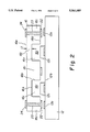
- FIG. 2 is a cross-sectional view of a ceramic protective cap and of a semiconductor device (e.g. a chip) with which the cap may be used; and
- FIG. 3(a)-(d) are cross-sectional views of a polyimide protective cap at various progressive stages of fabrication and attachment to a chip within a multi-chip module substrate.
- a multichip module 10 has a substrate 11 with a plurality of chip cavities 11a formed therein, through a top surface 11b thereof.
- An electronic component 12 such as an integrated circuit chip and the like, is disposed in each chipwell 11a.
- Electronic components 12 may be bonded to the substrate 11 with a layer of a thermoplastic adhesive 14.
- the electronic components 12 have contact pads 12a on an upper contact surface 12b thereof.
- Some of these electronic components 12 also have at least one sensitive structure 12c, such as an air bridge and the like, on upper surface 12b.
- a protective cap 16 is bonded to the component upper surface 12b, and has a recess 16r which surrounds, but does not touch the sensitive structure 12c to create an encapsulating volume 16v.
- Protective cap 16 is a protective "shield" structure comprising a cover-portion 16t having a top surface 16e and a bottom surface 16d, and a peripheral leg-portion 161 extending from the cover-portion bottom surface 16d to component surface 12b. Cover-portion 16t and leg-portion 161 cooperate to define a "U shaped" recess 16r. Recess 16r aligns with an associated sensitive structure 12c when the protective cap 16 is bonded to the device surface 12b.
- protective cap 16 covers the sensitive structure 12c on those sides (and top) not covered by the underlying chip 12, creating encapsulation volume 16v.
- Encapsulation volume 16v is large enough to ensure there is no contact between protective cap 16 and sensitive structure 12c, such that during lamination of the overlying HDI structure, the air bridge structure 12c is not damaged. Furthermore, the encapsulation volume 16v ensures that protective cap 16, as well as the overlying HDI structure, will not inhibit or impede the performance of sensitive structure 12c.
- protective cap 16 is designed to work in a multi-chip module 10 incorporating a high density interconnect structure 117, size limitations must be met. The protective cap 16 must not be so thick as to impede the lamination of the overlying HDI structure 117. However, the protective cap 16 will have some nominal thickness T which will extend above the air bridge structure 12c. Therefore, the chip well 11a in which the air bridge containing chip 12, with attached cap 16, is stationed, should be milled to a greater depth to offset this added thickness. Generally speaking, the protective cap 16 may be of two designs: a rigid ceramic or glass design, or a more flexible polyimide design.
- a first embodiment of protective cap 16 is illustrated in FIG. 2, where the cap 16 may be comprised of high temperature polymers, ceramics, such as alumina, aluminum nitride, etc., or glasses. Any insulative material which can withstand the temperature and pressure constraints of the HDI-structure lamination process is suitable for use as a protective cap 16.
- the first embodiment of protective cap 16 has recesses 16r which may be milled or formed through any conventional milling of molding techniques. Recesses 16r will be aligned with the air bridge structures 12c when protective cap 16 is attached to chip surface 12b. When protective cap 16 is bonded to chip surface 12b, each recess 16r creates an associated encapsulating volume 16v.
- Each encapsulating volume 16v includes the recess 16r within protective cap 16, as defined by the protective cap recess top 16a, the cap walls 16b and the chip surface 12b; encapsulation volume 16v also includes a lower surface defined by chip surface 12b and structure 12c, all of which are substantially devoid of HDI material.
- the protective cap 16 of FIG. 2 is bonded to the chip contact surface 12b by any suitable conductive adhesive material 22.
- This conductive adhesive suitable for use with the ceramic style protective cap 16 may be solder bumps, a conductive epoxy or any other suitable material which can electrically bond the cap 16 to the chip pads 12a on the chip surface 12b while at the same time provide electrical conductivity for later HDI interconnection.
- the first embodiment of protective cap 16 must have conductive posts 23 to provide for electrical conductivity from the bottom of the cap 16d to the top of the cap 16e.
- Posts 23 may be formed by etching through the thickness of the cap 16 in the associated leg-portion 161 (shown) or 16i (not shown) and then filling the etched holes with a conductive material, or may be made by forming the protective cap around a conductive post, i.e., molding a polymer around a copper wire post. It should be noted that as the thickness of the cap increases to greater than around 5 mils, it is difficult to form (etch or laser drill) a hole of small dimensions, such as 1 mil.
- Ceramics, glasses or other such brittle compositions tend to crack as their thicknesses decrease and are therefore not preferred cap 16 materials. Because recesses 16r in the design of the ceramic protective cap 16 create high stress points, trying to keep the thickness at a minimum, while ensuring structural integrity of the protective cap 16, is a non-trivial task. Therefore, this design is not the preferred embodiment.
- FIGS. 3(a)-(d) show the various fabrication stages of a second, and presently preferred, protective cap design, as well as illustrating the manner of attachment of the cap to the chip.
- the presently preferred protective cap 16 is fabricated from a polymer sheet by the following process.
- a carrier substrate 20 is precleaned by removing any contamination from at least one of its surfaces 20a and an adhesion promoter (not shown) may be added to surface 20a to achieve improved adhesion.
- substrate carrier 20 is preferably quartz for the reasons described hereinbelow, it is to be understood that any substrate material, e.g., plastic, ceramic, metal or glass, may be utilized.
- a release layer 26 is then deposited on substrate carrier surface 20a.
- a dielectric film 28 is then deposited on release layer 26. Dielectric film 28 may be applied from solution through spinning or spraying, or may be laminated by conventional techniques.
- Dielectric film 28 can be made from any number of materials which have a coefficient of thermal expansion matching that of the multichip module.
- a preferred material, for spin or spray application, is "PI-2611 Low Stress Polyimide", available from E.I. Du Pont De Numeours Co., Wilmington Del.
- Preferred materials for lamination include “Kapton-E®” also available from Du Pont, and "UBE Upilex” polyimide films, available from UBE Industries Ltd., Tokyo, Japan.
- Release layer 26 is "the adhesive” for lamination of dielectric film 28. As such, release layer 26 should be selected to both help bond dielectric film 28 to carrier substrate 20 and to permit subsequent release of dielectric layer 28 from carrier substrate 20.
- the upper bare surface 28a of dielectric film 28 is then prepared for application of an adhesive layer 30' by techniques such as reactive ion etching (RIE), a propanol jet scrub, or application of an adhesion promoter.
- Adhesive layer 30 is then applied to this "prepared" dielectric film 28.
- adhesive material 30 is selected to provide sufficient flow such that when it is bonded to chip surface 12b, a void free interface will form, but there will not be significant flowing of adhesive 30. Therefore, there will be no flowing of adhesive material 30 into any air bridge 12c regions.
- Adhesive layer 30 is then patterned with conventional photolithographic methods to allow subsequent removal of portions of adhesive layer 30, as well as portions of underlying dielectric layer 28. These removed regions, or recesses 16r will correspond to air bridge regions 12c when cap 16 is bonded to chip surface 12b.
- a "hard" mask layer 32 such as a sputtered film of 1000 ⁇ Titanium and 5000 ⁇ copper, deposit a layer of photoresist 34 which is subsequently patterned 36. This built-up structure with patterned photoresist is shown in FIG. 3(a).
- Mask Layer 32 can then be etched away where photoresist 34 was patterned 36, leaving adhesive layer 30 exposed.
- Photoresist 34 is then removed, and reactive ion etching, or any other appropriate method may be used to remove the exposed regions of adhesive layer 30, and a portion of dielectric layer 28, to a predetermined thickness, to create recesses 16r.
- Removal of mask layer 32 leaves a completed protective cap 16 attached to its carrier substrate 20, as shown in FIG. 3(b).
- This figure shows recesses 16r, etched through both adhesive layer 30 and a portion of polyimide layer 28, which will align with an associated air bridge structure 12c when cap 16 is bonded to chip surface 12b.
- a temporary polymeric film stencil can be used as the temporary "hard” mask 32.
- the polymeric film may comprise a 2 to 5 mil thick "Kapton" polyimide film, and the appropriate mask openings can be generated by laser cutting.
- the polymeric mask 32 can be easily attached and removed from the adhesive layer 30.
- Protective cap 16, attached to carrier substrate 20, is then aligned with multi-chip module substrate 11 such that recesses 16r are aligned with associated air bridge 12c structures, and then bonded to form encapsulating volumes 16v, as shown in FIG. 3(c).
- This alignment and attachment may be accomplished with any conventional die placement machine. Attachment of protective cap 16 will be accomplished at temperatures and pressures necessary to bond adhesive 30, while maintaining alignment.
- Adhesive 30 preferably has a melt viscosity which, upon bonding allows formation of a void-free bond between protective cap 16 and chip surface 12b. Adhesive 30 should not be so low in viscosity as to infiltrate air bridge structure 12c.
- Carrier substrate 20 is then separated from its protective cap 16 before lamination of the HDI structure 117. This separation is facilitated because release layer 26 was previously disposed between the carrier substrate 20 and polymer layer 28 to increase the efficiency of separation.
- carrier layer 20 is quartz
- protective cap 16 may be separated by exposing carrier substrate backside 20b to a pulsed excimer laser. UV output of the laser is transmitted through carrier substrate backside 20b and is absorbed at release layer 26, i.e., at interface of the quartz carrier 20a and polyimide 28.
- release layer 26 is designed to enhance the absorption of UV radiation.
- Preferred release layer materials which enhance the absorption of UV radiation are thin films (100 ⁇ ) of metals such as titanium, titanium/tungsten, or indium-tin-oxide (ITO).
- any material which enhances UV absorption and does not interfere with the bonding of polyimide 28 to carrier substrate 20 may be utilized. Absorption of UV radiation causes quartz substrate 20 to release from dielectric layer 28, yielding a protective cap 16 bonded to chip 12 and separate from its carrier substrate 20.
- release layer 26 would comprise a material which would dissolve in a solvent which would not adversely affect the multi-chip module.
- release layer 26 are fluorinated polymers, or any other material which dissolves in a solvent which has substantially no adverse affect on module 10.
- protective cap top surface 16e is preferably in the same plane as substrate surface 11b. And, as described above, chip well 11a was made deeper to allow for the added thickness of protective cap 16. This design ensures that protective cap 16 has no adverse affects on the HDI structure lamination.
- each recess 16r is aligned with and encloses an associated air bridge structure 12c, thereby creating encapsulating volume 16v. Encapsulation volume is large enough to ensure that the protective cap 16 does not interfere with, or impede, the performance of sensitive structure.
- protective cap design i.e., a first embodiment with conductive posts and solder bumps, or a presently preferred embodiment with via interconnections to the chip pads, it must allow for lamination of a high density interconnect structure.
- high density interconnect structure 117 is fabricated above chips 12 and sensitive structures 12c (covered by protective cap 16). Since protective cap top 16e is in the same plane as substrate surface 11b, the lamination of the first dielectric layer is accomplished in any conventional manner.
- a first stratum 118 of high density interconnect structure 117 comprises a dielectric layer 120 supporting a patterned metallization layer 122.
- Dielectric layer 120 has separate lower and upper sublayers 124 and 126, respectively, and supports patterned metallization layer 122 which makes electrical contact with contact pads 12b on substrate 11 within via holes 127 in dielectric layer 120.
- the lower dielectric sublayer 124 is a thermoplastic adhesive which allows subsequent processing at temperatures below 260° C. As referenced hereinabove, U.S. Pat. No.
- Ultem is a trademark of General Electric Co, Pittsfield, Mass., for a polyetherimide resin
- Benzoflex is a trademark of Velsicol Chemical Corp., Rosemont, Ill., for pentaerythritol tetrabenzoate.
- Upper dielectric sublayer 126 is preferably a thermoset material (for example, a KAPTON® film). Other materials, including thermoplastics which exhibit sufficient stability, may also be used for the upper dielectric sublayer 126.
- metallization layer 122 makes electrical contact with at least some contact pads 12a on substrate 11. If the chip pads 12a to be connected are below protective cap 16, the electrical connection must not only be made through dielectric layer 120 but also through protective cap 16. If protective cap 16 comprises a ceramic or glass, electrical interconnection will be made by forming via holes 127 through dielectric layer 120 to make connection with a selected electrical pad 24 on top of cap 16 (see FIG. 2). Pad 24 is electrically connected to chip pad 12a through electrical post 23 in protective cap 16. If, however, the presently preferred protective cap 16 comprising polyimide is utilized, via holes 127 must extend both through dielectric layer 120 and protective cap 16 to make electrical connection with chip pads 12a.
- Second and higher strata may be formed by conventional techniques, such as those described in above described co-pending application Ser. No. 08/308,886, filed Sep. 19, 1994.
- a siloxane polyimide/epoxy (SPIE) adhesive system may be used for these higher strata, as described in commonly assigned U.S. Pat. No. 5,161,093, issued Nov. 3, 1992, to Gorczyca et al, which is herein incorporated by reference in its entirety.
- the SPIE crosslinking copolymer blend adhesive materials used as the lower dielectric sublayer in the second and higher strata are selected so that these adhesive materials become set at a low enough temperature that curing the adhesive materials has no adverse effect on the high density interconnect structure or the electronic components being connected thereby. Correct selection of the curing properties of the adhesive materials allows the structure to be fabricated and, if need be, disassembled and reassembled without an adverse effect on the electronic components being interconnected.
- protective cap 16 need not be removed from below the high density interconnect structure, there is no need to use any form of removal process for HDI structure 117 to expose cap 16; thus, neither chemical etch nor laser ablation of the high density interconnect structure 117 is necessary. More importantly, there are no limitations placed on the routing of the metallization layers, and in fact, the protective cap provides additional area in which to route metallization. For example, the top and sides of the protective cap may have additional metallization layers which can be patterned to provide alternate circuits for coupling, power or ground planes, etc. Furthermore, the air bridge structure 12c is not exposed to any of the conventional high density interconnect structure removal processes, such as laser ablation and plasma-ashing. This is a significant advantage in producing a highly reliable module.
- the fabricated module may be complete; various metallization layers 122, 132, 144 will carry power, ground, and at least one set of signal conductors. And since none of the high density interconnect structure is removed, there are few limitations on how the metallization layers must be routed.
Landscapes
- Engineering & Computer Science (AREA)
- Computer Hardware Design (AREA)
- Microelectronics & Electronic Packaging (AREA)
- Power Engineering (AREA)
- Physics & Mathematics (AREA)
- Condensed Matter Physics & Semiconductors (AREA)
- General Physics & Mathematics (AREA)
- Internal Circuitry In Semiconductor Integrated Circuit Devices (AREA)
- Wire Bonding (AREA)
Abstract
Description
Claims (8)
Priority Applications (4)
Application Number | Priority Date | Filing Date | Title |
---|---|---|---|
US08/359,128 US5561085A (en) | 1994-12-19 | 1994-12-19 | Structure for protecting air bridges on semiconductor chips from damage |
EP95309042A EP0718885A3 (en) | 1994-12-19 | 1995-12-12 | Structure for protecting air bridges on semiconductor chips from damage |
JP7348827A JPH08236628A (en) | 1994-12-19 | 1995-12-19 | Structure for protecting air bridge on semiconductor chip from damage |
US08/663,506 US5757072A (en) | 1994-12-19 | 1996-06-14 | Structure for protecting air bridges on semiconductor chips from damage |
Applications Claiming Priority (1)
Application Number | Priority Date | Filing Date | Title |
---|---|---|---|
US08/359,128 US5561085A (en) | 1994-12-19 | 1994-12-19 | Structure for protecting air bridges on semiconductor chips from damage |
Related Child Applications (1)
Application Number | Title | Priority Date | Filing Date |
---|---|---|---|
US08/663,506 Division US5757072A (en) | 1994-12-19 | 1996-06-14 | Structure for protecting air bridges on semiconductor chips from damage |
Publications (1)
Publication Number | Publication Date |
---|---|
US5561085A true US5561085A (en) | 1996-10-01 |
Family
ID=23412436
Family Applications (2)
Application Number | Title | Priority Date | Filing Date |
---|---|---|---|
US08/359,128 Expired - Fee Related US5561085A (en) | 1994-12-19 | 1994-12-19 | Structure for protecting air bridges on semiconductor chips from damage |
US08/663,506 Expired - Lifetime US5757072A (en) | 1994-12-19 | 1996-06-14 | Structure for protecting air bridges on semiconductor chips from damage |
Family Applications After (1)
Application Number | Title | Priority Date | Filing Date |
---|---|---|---|
US08/663,506 Expired - Lifetime US5757072A (en) | 1994-12-19 | 1996-06-14 | Structure for protecting air bridges on semiconductor chips from damage |
Country Status (3)
Country | Link |
---|---|
US (2) | US5561085A (en) |
EP (1) | EP0718885A3 (en) |
JP (1) | JPH08236628A (en) |
Cited By (34)
Publication number | Priority date | Publication date | Assignee | Title |
---|---|---|---|---|
US5801074A (en) * | 1996-02-20 | 1998-09-01 | Kim; Jong Tae | Method of making an air tight cavity in an assembly package |
US5943558A (en) * | 1996-09-23 | 1999-08-24 | Communications Technology, Inc. | Method of making an assembly package having an air tight cavity and a product made by the method |
US6077757A (en) * | 1997-05-15 | 2000-06-20 | Nec Corporation | Method of forming chip semiconductor devices |
US6087199A (en) * | 1998-02-04 | 2000-07-11 | International Business Machines Corporation | Method for fabricating a very dense chip package |
US6222263B1 (en) * | 1999-10-19 | 2001-04-24 | International Business Machines Corporation | Chip assembly with load-bearing lid in thermal contact with the chip |
US6255137B1 (en) | 1999-07-01 | 2001-07-03 | Lockheed Martin Corp. | Method for making air pockets in an HDI context |
US20020003304A1 (en) * | 2000-07-07 | 2002-01-10 | Kabushiki Kaisha Toshiba | Semiconductor device having multilevel interconnection |
US6507110B1 (en) * | 2000-03-08 | 2003-01-14 | Teledyne Technologies Incorporated | Microwave device and method for making same |
US6531232B1 (en) * | 1998-10-29 | 2003-03-11 | Commissariat A L'energie Atomique | System for assembling substrates to bonding zones provided with cavities |
DE10216267A1 (en) * | 2002-04-12 | 2003-10-30 | Infineon Technologies Ag | Method for producing a housing for a chip with a micromechanical structure |
US20040007776A1 (en) * | 2002-07-11 | 2004-01-15 | Tong Chen | Multi-substrate layer semiconductor packages and method for making same |
US6730571B1 (en) | 1999-10-14 | 2004-05-04 | Chartered Semiconductor Manufacturing Ltd. | Method to form a cross network of air gaps within IMD layer |
EP1447850A2 (en) * | 2003-02-13 | 2004-08-18 | Shinko Electric Industries Co., Ltd. | Electronic parts packaging structure and method of manufacturing the same |
US6819566B1 (en) * | 2002-10-25 | 2004-11-16 | International Business Machines Corporation | Grounding and thermal dissipation for integrated circuit packages |
US20060099733A1 (en) * | 2004-11-09 | 2006-05-11 | Geefay Frank S | Semiconductor package and fabrication method |
US20060163726A1 (en) * | 2004-11-12 | 2006-07-27 | Oliver Kierse | Spaced, bumped component structure |
US20070085195A1 (en) * | 2005-10-19 | 2007-04-19 | Samsung Electronics Co., Ltd. | Wafer level packaging cap and fabrication method thereof |
US20080258311A1 (en) * | 2007-04-23 | 2008-10-23 | Kabushiki Kaisha Toshiba | Semiconductor device and method of manufacturing the same |
US7485562B2 (en) * | 2002-08-27 | 2009-02-03 | Micron Technology, Inc. | Method of making multichip wafer level packages and computing systems incorporating same |
US7656236B2 (en) | 2007-05-15 | 2010-02-02 | Teledyne Wireless, Llc | Noise canceling technique for frequency synthesizer |
US20100112756A1 (en) * | 2008-11-06 | 2010-05-06 | Amrine Craig S | Integrated circuit package formation |
US8008130B2 (en) * | 1999-10-05 | 2011-08-30 | Renesas Electronics Corporation | Multilayer interconnection board, semiconductor device having the same, and method of forming the same as well as method of mounting the semicondutor chip on the interconnection board |
US8179045B2 (en) | 2008-04-22 | 2012-05-15 | Teledyne Wireless, Llc | Slow wave structure having offset projections comprised of a metal-dielectric composite stack |
CN104377172A (en) * | 2013-07-26 | 2015-02-25 | 英飞凌科技股份有限公司 | Chip Package with Embedded Passive Component |
US20150102490A1 (en) * | 2011-01-31 | 2015-04-16 | Avago Technologies General Ip (Singapore) Pte. Ltd. | Semiconductor device having an airbridge and method of fabricating the same |
US9202660B2 (en) | 2013-03-13 | 2015-12-01 | Teledyne Wireless, Llc | Asymmetrical slow wave structures to eliminate backward wave oscillations in wideband traveling wave tubes |
US20170094798A1 (en) * | 2014-06-23 | 2017-03-30 | Murata Manufacturing Co., Ltd. | Component incorporating substrate and method for manufacturing component incorporating substrate |
WO2017139542A1 (en) * | 2016-02-11 | 2017-08-17 | Skyworks Solutions, Inc. | Device packaging using a recyclable carrier substrate |
US20190082543A1 (en) * | 2014-02-27 | 2019-03-14 | At&S Austria Technologie & Systemtechnik Aktiengesellschaft | Method for Making Contact with a Component Embedded in a Printed Circuit Board |
US10453763B2 (en) | 2016-08-10 | 2019-10-22 | Skyworks Solutions, Inc. | Packaging structures with improved adhesion and strength |
US10779413B2 (en) | 2013-12-12 | 2020-09-15 | At&S Austria Technologie & Systemtechnik Aktiengesellschaft | Method of embedding a component in a printed circuit board |
US11172576B2 (en) | 2013-11-27 | 2021-11-09 | At&S Austria Technologie & Systemtechnik Aktiengesellschaft | Method for producing a printed circuit board structure |
US11348865B2 (en) * | 2019-09-30 | 2022-05-31 | Intel Corporation | Electronic device including a substrate having interconnects |
US20220304163A1 (en) * | 2021-03-19 | 2022-09-22 | Ajinomoto Co., Inc. | Method for making printed wiring board, printed wiring board, and adhesive film for making printed wiring board |
Families Citing this family (64)
Publication number | Priority date | Publication date | Assignee | Title |
---|---|---|---|---|
US5841193A (en) * | 1996-05-20 | 1998-11-24 | Epic Technologies, Inc. | Single chip modules, repairable multichip modules, and methods of fabrication thereof |
JP2842378B2 (en) * | 1996-05-31 | 1999-01-06 | 日本電気株式会社 | High-density mounting structure for electronic circuit boards |
US5856914A (en) * | 1996-07-29 | 1999-01-05 | National Semiconductor Corporation | Micro-electronic assembly including a flip-chip mounted micro-device and method |
DE19640594B4 (en) * | 1996-10-01 | 2016-08-04 | Osram Gmbh | module |
JP3695893B2 (en) * | 1996-12-03 | 2005-09-14 | 沖電気工業株式会社 | Semiconductor device, manufacturing method and mounting method thereof |
JP2962272B2 (en) * | 1997-04-18 | 1999-10-12 | 日本電気株式会社 | Method for manufacturing semiconductor device |
US6143396A (en) * | 1997-05-01 | 2000-11-07 | Texas Instruments Incorporated | System and method for reinforcing a bond pad |
US5880528A (en) * | 1997-09-30 | 1999-03-09 | Intel Corporation | Energy absorbing structures to prevent damage to an integrated circuit |
US5969421A (en) * | 1997-11-18 | 1999-10-19 | Lucent Technologies Inc. | Integrated circuit conductors that avoid current crowding |
US6143655A (en) * | 1998-02-25 | 2000-11-07 | Micron Technology, Inc. | Methods and structures for silver interconnections in integrated circuits |
US6121126A (en) * | 1998-02-25 | 2000-09-19 | Micron Technologies, Inc. | Methods and structures for metal interconnections in integrated circuits |
US5920121A (en) * | 1998-02-25 | 1999-07-06 | Micron Technology, Inc. | Methods and structures for gold interconnections in integrated circuits |
US6492694B2 (en) | 1998-02-27 | 2002-12-10 | Micron Technology, Inc. | Highly conductive composite polysilicon gate for CMOS integrated circuits |
US6815303B2 (en) * | 1998-04-29 | 2004-11-09 | Micron Technology, Inc. | Bipolar transistors with low-resistance emitter contacts |
US6239980B1 (en) * | 1998-08-31 | 2001-05-29 | General Electric Company | Multimodule interconnect structure and process |
JP3214470B2 (en) | 1998-11-16 | 2001-10-02 | 日本電気株式会社 | Multi-chip module and manufacturing method thereof |
DE19858759C1 (en) * | 1998-12-18 | 2000-03-23 | Siemens Ag | Integrated circuit with nanoscale devices and CMOS device |
US6495399B1 (en) * | 1999-11-01 | 2002-12-17 | Chartered Semiconductor Manufacturing Ltd. | Method of vacuum packaging a semiconductor device assembly |
JP4251421B2 (en) * | 2000-01-13 | 2009-04-08 | 新光電気工業株式会社 | Manufacturing method of semiconductor device |
WO2001063991A1 (en) * | 2000-02-25 | 2001-08-30 | Ibiden Co., Ltd. | Multilayer printed wiring board and method for producing multilayer printed wiring board |
US6509622B1 (en) | 2000-08-23 | 2003-01-21 | Intel Corporation | Integrated circuit guard ring structures |
TW455965B (en) * | 2000-08-29 | 2001-09-21 | Phoenix Prec Technology Corp | Method for forming solder bumpers on IC package substrate and structure formed by the same |
US6480385B2 (en) | 2000-09-13 | 2002-11-12 | Intel Corporation | Electronic assembly and cooling thereof |
KR100797422B1 (en) * | 2000-09-25 | 2008-01-23 | 이비덴 가부시키가이샤 | Semiconductor element, method of manufacturing semiconductor element, multi-layer printed circuit board, and method of manufacturing multi-layer printed circuit board |
US6862189B2 (en) * | 2000-09-26 | 2005-03-01 | Kabushiki Kaisha Toshiba | Electronic component, circuit device, method for manufacturing the circuit device, and semiconductor device |
US6690081B2 (en) * | 2000-11-18 | 2004-02-10 | Georgia Tech Research Corporation | Compliant wafer-level packaging devices and methods of fabrication |
US6773962B2 (en) * | 2001-03-15 | 2004-08-10 | General Electric Company | Microelectromechanical system device packaging method |
US7498196B2 (en) * | 2001-03-30 | 2009-03-03 | Megica Corporation | Structure and manufacturing method of chip scale package |
US6706624B1 (en) * | 2001-10-31 | 2004-03-16 | Lockheed Martin Corporation | Method for making multichip module substrates by encapsulating electrical conductors |
TW584950B (en) | 2001-12-31 | 2004-04-21 | Megic Corp | Chip packaging structure and process thereof |
TW503496B (en) * | 2001-12-31 | 2002-09-21 | Megic Corp | Chip packaging structure and manufacturing process of the same |
TW544882B (en) | 2001-12-31 | 2003-08-01 | Megic Corp | Chip package structure and process thereof |
US6673698B1 (en) * | 2002-01-19 | 2004-01-06 | Megic Corporation | Thin film semiconductor package utilizing a glass substrate with composite polymer/metal interconnect layers |
TW517361B (en) * | 2001-12-31 | 2003-01-11 | Megic Corp | Chip package structure and its manufacture process |
JP3875568B2 (en) * | 2002-02-05 | 2007-01-31 | 株式会社東芝 | Semiconductor device and manufacturing method thereof |
FR2837982B1 (en) * | 2002-03-26 | 2005-02-18 | Thales Sa | INTEGRATED CIRCUIT MODULE AND METHOD FOR MANUFACTURING THE SAME |
US7061100B2 (en) * | 2002-04-03 | 2006-06-13 | Matsushita Electric Industrial Co., Ltd. | Semiconductor built-in millimeter-wave band module |
CA2464078C (en) * | 2002-08-09 | 2010-01-26 | Casio Computer Co., Ltd. | Semiconductor device and method of manufacturing the same |
US6674168B1 (en) * | 2003-01-21 | 2004-01-06 | International Business Machines Corporation | Single and multilevel rework |
US7135780B2 (en) | 2003-02-12 | 2006-11-14 | Micron Technology, Inc. | Semiconductor substrate for build-up packages |
DE10355925B4 (en) * | 2003-11-29 | 2006-07-06 | Semikron Elektronik Gmbh & Co. Kg | Power semiconductor module and method of its manufacture |
JP4885426B2 (en) * | 2004-03-12 | 2012-02-29 | ルネサスエレクトロニクス株式会社 | Semiconductor memory device, semiconductor device and manufacturing method thereof |
JP4361826B2 (en) * | 2004-04-20 | 2009-11-11 | 新光電気工業株式会社 | Semiconductor device |
US20060211233A1 (en) * | 2005-03-21 | 2006-09-21 | Skyworks Solutions, Inc. | Method for fabricating a wafer level package having through wafer vias for external package connectivity and related structure |
US7576426B2 (en) * | 2005-04-01 | 2009-08-18 | Skyworks Solutions, Inc. | Wafer level package including a device wafer integrated with a passive component |
KR100661169B1 (en) * | 2005-06-03 | 2006-12-26 | 삼성전자주식회사 | Packaging chip and packaging method thereof |
TWI262565B (en) * | 2005-10-31 | 2006-09-21 | Ind Tech Res Inst | Protecting structure and method for manufacturing electronic packaging joints |
JP5343301B2 (en) * | 2005-11-28 | 2013-11-13 | 三菱電機株式会社 | Semiconductor device and manufacturing method thereof |
US7635606B2 (en) * | 2006-08-02 | 2009-12-22 | Skyworks Solutions, Inc. | Wafer level package with cavities for active devices |
US20080217708A1 (en) * | 2007-03-09 | 2008-09-11 | Skyworks Solutions, Inc. | Integrated passive cap in a system-in-package |
US7919839B2 (en) * | 2007-07-24 | 2011-04-05 | Northrop Grumman Systems Corporation | Support structures for on-wafer testing of wafer-level packages and multiple wafer stacked structures |
CN101878527B (en) * | 2007-11-30 | 2012-09-26 | 斯盖沃克斯瑟路申斯公司 | Wafer level packaging using flip chip mounting |
US8900931B2 (en) | 2007-12-26 | 2014-12-02 | Skyworks Solutions, Inc. | In-situ cavity integrated circuit package |
US7952187B2 (en) * | 2008-03-31 | 2011-05-31 | General Electric Company | System and method of forming a wafer scale package |
US8349653B2 (en) * | 2010-06-02 | 2013-01-08 | Maxim Integrated Products, Inc. | Use of device assembly for a generalization of three-dimensional metal interconnect technologies |
US8623699B2 (en) * | 2010-07-26 | 2014-01-07 | General Electric Company | Method of chip package build-up |
CN102404935B (en) * | 2010-09-13 | 2014-07-02 | 巨擘科技股份有限公司 | Multilayered through hole laminating structure |
JP5827476B2 (en) * | 2011-03-08 | 2015-12-02 | 株式会社東芝 | Semiconductor module and manufacturing method thereof |
US8581406B1 (en) * | 2012-04-20 | 2013-11-12 | Raytheon Company | Flip chip mounted monolithic microwave integrated circuit (MMIC) structure |
US8664743B1 (en) * | 2012-10-31 | 2014-03-04 | Taiwan Semiconductor Manufacturing Company, Ltd. | Air-gap formation in interconnect structures |
US9093563B2 (en) | 2013-07-11 | 2015-07-28 | International Business Machines Corporation | Electronic module assembly with patterned adhesive array |
US9190389B2 (en) | 2013-07-26 | 2015-11-17 | Infineon Technologies Ag | Chip package with passives |
CN110164978B (en) * | 2018-02-14 | 2022-06-21 | 联华电子股份有限公司 | Semiconductor device and method for manufacturing the same |
JP2022049352A (en) * | 2020-09-16 | 2022-03-29 | 浜松ホトニクス株式会社 | Photodetection module and beat spectroscopic device |
Citations (16)
Publication number | Priority date | Publication date | Assignee | Title |
---|---|---|---|---|
US4466181A (en) * | 1981-12-04 | 1984-08-21 | Clarion Co., Ltd. | Method for mounting conjoined devices |
US4783695A (en) * | 1986-09-26 | 1988-11-08 | General Electric Company | Multichip integrated circuit packaging configuration and method |
US4835704A (en) * | 1986-12-29 | 1989-05-30 | General Electric Company | Adaptive lithography system to provide high density interconnect |
US4878991A (en) * | 1988-12-12 | 1989-11-07 | General Electric Company | Simplified method for repair of high density interconnect circuits |
US4894115A (en) * | 1989-02-14 | 1990-01-16 | General Electric Company | Laser beam scanning method for forming via holes in polymer materials |
US4933042A (en) * | 1986-09-26 | 1990-06-12 | General Electric Company | Method for packaging integrated circuit chips employing a polymer film overlay layer |
US5161093A (en) * | 1990-07-02 | 1992-11-03 | General Electric Company | Multiple lamination high density interconnect process and structure employing a variable crosslinking adhesive |
US5192716A (en) * | 1989-01-25 | 1993-03-09 | Polylithics, Inc. | Method of making a extended integration semiconductor structure |
US5280192A (en) * | 1990-04-30 | 1994-01-18 | International Business Machines Corporation | Three-dimensional memory card structure with internal direct chip attachment |
US5306670A (en) * | 1993-02-09 | 1994-04-26 | Texas Instruments Incorporated | Multi-chip integrated circuit module and method for fabrication thereof |
US5331203A (en) * | 1990-04-05 | 1994-07-19 | General Electric Company | High density interconnect structure including a chamber |
US5338975A (en) * | 1990-07-02 | 1994-08-16 | General Electric Company | High density interconnect structure including a spacer structure and a gap |
US5354714A (en) * | 1991-08-01 | 1994-10-11 | Texas Instruments Incorporated | Method of forming a vacuum micro-chamber for encapsulating a microelectronics device |
US5353498A (en) * | 1993-02-08 | 1994-10-11 | General Electric Company | Method for fabricating an integrated circuit module |
US5401688A (en) * | 1991-02-18 | 1995-03-28 | Kabushiki Kaisha Toshiba | Semiconductor device of multichip module-type |
US5432681A (en) * | 1993-04-30 | 1995-07-11 | The United States Of America As Represented By The Secretary Of The Air Force | Density improvement for planar hybrid wafer scale integration |
Family Cites Families (20)
Publication number | Priority date | Publication date | Assignee | Title |
---|---|---|---|---|
US4629993A (en) | 1985-04-15 | 1986-12-16 | The University Of Rochester | Pockels cell driver |
KR910001419B1 (en) * | 1987-03-31 | 1991-03-05 | 가부시키가이샤 도시바 | Resin sealed intergrated circuit device |
JPH01157557A (en) * | 1987-09-07 | 1989-06-20 | Sumitomo Electric Ind Ltd | Semiconductor and its manufacture |
US5108825A (en) | 1989-12-21 | 1992-04-28 | General Electric Company | Epoxy/polyimide copolymer blend dielectric and layered circuits incorporating it |
JPH03211757A (en) * | 1989-12-21 | 1991-09-17 | General Electric Co <Ge> | Hermetically sealed object |
US5169678A (en) | 1989-12-26 | 1992-12-08 | General Electric Company | Laser ablatable polymer dielectrics and methods |
US5127998A (en) | 1990-01-02 | 1992-07-07 | General Electric Company | Area-selective metallization process |
US5355102A (en) | 1990-04-05 | 1994-10-11 | General Electric Company | HDI impedance matched microwave circuit assembly |
FI88229C (en) | 1990-04-12 | 1993-04-13 | Nokia Mobile Phones Ltd | Connector piece for insert adapter |
US5073814A (en) * | 1990-07-02 | 1991-12-17 | General Electric Company | Multi-sublayer dielectric layers |
US5049978A (en) * | 1990-09-10 | 1991-09-17 | General Electric Company | Conductively enclosed hybrid integrated circuit assembly using a silicon substrate |
US5507903A (en) * | 1991-03-12 | 1996-04-16 | Sumitomo Bakelite Company Limited | Process for producing two-layered tape for tab |
US5151769A (en) * | 1991-04-04 | 1992-09-29 | General Electric Company | Optically patterned RF shield for an integrated circuit chip for analog and/or digital operation at microwave frequencies |
CA2071662A1 (en) * | 1991-06-26 | 1992-12-27 | Jon J. Gulick | Integrated socket-type package for flip-chip semiconductor devices and circuits |
EP0524823B1 (en) | 1991-07-26 | 1999-10-06 | Kureha Chemical Industry Co., Ltd. | A resin composition and food packaging materials formed therefrom |
JPH05291319A (en) * | 1992-04-07 | 1993-11-05 | Toshiba Corp | Resin sealing-type semiconductor device |
JPH06163628A (en) * | 1992-11-20 | 1994-06-10 | Toshiba Corp | Semiconductor integrated circuit |
US5300812A (en) | 1992-12-09 | 1994-04-05 | General Electric Company | Plasticized polyetherimide adhesive composition and usage |
US5548099A (en) * | 1994-09-13 | 1996-08-20 | Martin Marietta Corporation | Method for making an electronics module having air bridge protection without large area ablation |
US5524339A (en) * | 1994-09-19 | 1996-06-11 | Martin Marietta Corporation | Method for protecting gallium arsenide mmic air bridge structures |
-
1994
- 1994-12-19 US US08/359,128 patent/US5561085A/en not_active Expired - Fee Related
-
1995
- 1995-12-12 EP EP95309042A patent/EP0718885A3/en not_active Withdrawn
- 1995-12-19 JP JP7348827A patent/JPH08236628A/en active Pending
-
1996
- 1996-06-14 US US08/663,506 patent/US5757072A/en not_active Expired - Lifetime
Patent Citations (16)
Publication number | Priority date | Publication date | Assignee | Title |
---|---|---|---|---|
US4466181A (en) * | 1981-12-04 | 1984-08-21 | Clarion Co., Ltd. | Method for mounting conjoined devices |
US4783695A (en) * | 1986-09-26 | 1988-11-08 | General Electric Company | Multichip integrated circuit packaging configuration and method |
US4933042A (en) * | 1986-09-26 | 1990-06-12 | General Electric Company | Method for packaging integrated circuit chips employing a polymer film overlay layer |
US4835704A (en) * | 1986-12-29 | 1989-05-30 | General Electric Company | Adaptive lithography system to provide high density interconnect |
US4878991A (en) * | 1988-12-12 | 1989-11-07 | General Electric Company | Simplified method for repair of high density interconnect circuits |
US5192716A (en) * | 1989-01-25 | 1993-03-09 | Polylithics, Inc. | Method of making a extended integration semiconductor structure |
US4894115A (en) * | 1989-02-14 | 1990-01-16 | General Electric Company | Laser beam scanning method for forming via holes in polymer materials |
US5331203A (en) * | 1990-04-05 | 1994-07-19 | General Electric Company | High density interconnect structure including a chamber |
US5280192A (en) * | 1990-04-30 | 1994-01-18 | International Business Machines Corporation | Three-dimensional memory card structure with internal direct chip attachment |
US5161093A (en) * | 1990-07-02 | 1992-11-03 | General Electric Company | Multiple lamination high density interconnect process and structure employing a variable crosslinking adhesive |
US5338975A (en) * | 1990-07-02 | 1994-08-16 | General Electric Company | High density interconnect structure including a spacer structure and a gap |
US5401688A (en) * | 1991-02-18 | 1995-03-28 | Kabushiki Kaisha Toshiba | Semiconductor device of multichip module-type |
US5354714A (en) * | 1991-08-01 | 1994-10-11 | Texas Instruments Incorporated | Method of forming a vacuum micro-chamber for encapsulating a microelectronics device |
US5353498A (en) * | 1993-02-08 | 1994-10-11 | General Electric Company | Method for fabricating an integrated circuit module |
US5306670A (en) * | 1993-02-09 | 1994-04-26 | Texas Instruments Incorporated | Multi-chip integrated circuit module and method for fabrication thereof |
US5432681A (en) * | 1993-04-30 | 1995-07-11 | The United States Of America As Represented By The Secretary Of The Air Force | Density improvement for planar hybrid wafer scale integration |
Cited By (57)
Publication number | Priority date | Publication date | Assignee | Title |
---|---|---|---|---|
US5801074A (en) * | 1996-02-20 | 1998-09-01 | Kim; Jong Tae | Method of making an air tight cavity in an assembly package |
US5943558A (en) * | 1996-09-23 | 1999-08-24 | Communications Technology, Inc. | Method of making an assembly package having an air tight cavity and a product made by the method |
US6077757A (en) * | 1997-05-15 | 2000-06-20 | Nec Corporation | Method of forming chip semiconductor devices |
US6087199A (en) * | 1998-02-04 | 2000-07-11 | International Business Machines Corporation | Method for fabricating a very dense chip package |
US6531232B1 (en) * | 1998-10-29 | 2003-03-11 | Commissariat A L'energie Atomique | System for assembling substrates to bonding zones provided with cavities |
US6255137B1 (en) | 1999-07-01 | 2001-07-03 | Lockheed Martin Corp. | Method for making air pockets in an HDI context |
EP1065716A3 (en) * | 1999-07-01 | 2005-11-30 | Lockheed Martin Corporation | Method for making air pockets in an HDI context |
US8008130B2 (en) * | 1999-10-05 | 2011-08-30 | Renesas Electronics Corporation | Multilayer interconnection board, semiconductor device having the same, and method of forming the same as well as method of mounting the semicondutor chip on the interconnection board |
US7112866B2 (en) | 1999-10-14 | 2006-09-26 | Chartered Semiconductor Manufacturing Ltd. | Method to form a cross network of air gaps within IMD layer |
US6730571B1 (en) | 1999-10-14 | 2004-05-04 | Chartered Semiconductor Manufacturing Ltd. | Method to form a cross network of air gaps within IMD layer |
US20040175896A1 (en) * | 1999-10-14 | 2004-09-09 | Chartered Semiconductor Manufacturing Ltd. | Method to form a cross network of air gaps within IMD layer |
US6222263B1 (en) * | 1999-10-19 | 2001-04-24 | International Business Machines Corporation | Chip assembly with load-bearing lid in thermal contact with the chip |
US6507110B1 (en) * | 2000-03-08 | 2003-01-14 | Teledyne Technologies Incorporated | Microwave device and method for making same |
US20020003304A1 (en) * | 2000-07-07 | 2002-01-10 | Kabushiki Kaisha Toshiba | Semiconductor device having multilevel interconnection |
DE10216267A1 (en) * | 2002-04-12 | 2003-10-30 | Infineon Technologies Ag | Method for producing a housing for a chip with a micromechanical structure |
US7011986B2 (en) | 2002-04-12 | 2006-03-14 | Infineon Technologies Ag | Method for manufacturing a housing for a chip with a micromechanical structure |
DE10216267B4 (en) * | 2002-04-12 | 2005-04-14 | Infineon Technologies Ag | Method for producing a housing for a chip with a micromechanical structure |
US20050106785A1 (en) * | 2002-04-12 | 2005-05-19 | Frank Daeche | Method for manufacturing a housing for a chip with a micromechanical structure |
US20040007776A1 (en) * | 2002-07-11 | 2004-01-15 | Tong Chen | Multi-substrate layer semiconductor packages and method for making same |
US6933603B2 (en) | 2002-07-11 | 2005-08-23 | Teledyne Technologies Incorporated | Multi-substrate layer semiconductor packages and method for making same |
US7485562B2 (en) * | 2002-08-27 | 2009-02-03 | Micron Technology, Inc. | Method of making multichip wafer level packages and computing systems incorporating same |
US20040233638A1 (en) * | 2002-10-25 | 2004-11-25 | International Business Machines Corporation | Improvements in grounding and thermal dissipation for integrated circuit packages |
US6819566B1 (en) * | 2002-10-25 | 2004-11-16 | International Business Machines Corporation | Grounding and thermal dissipation for integrated circuit packages |
US20090206471A1 (en) * | 2003-02-13 | 2009-08-20 | Shinko Electric Industries Co., Ltd. | Electronic parts packaging structure and method of manufacturing the same |
EP1447850A2 (en) * | 2003-02-13 | 2004-08-18 | Shinko Electric Industries Co., Ltd. | Electronic parts packaging structure and method of manufacturing the same |
US7964950B2 (en) | 2003-02-13 | 2011-06-21 | Shinko Electric Industries Co., Ltd. | Electronic parts packaging structure and method of manufacturing the same |
EP1447850A3 (en) * | 2003-02-13 | 2010-07-21 | Shinko Electric Industries Co., Ltd. | Electronic parts packaging structure and method of manufacturing the same |
US20060099733A1 (en) * | 2004-11-09 | 2006-05-11 | Geefay Frank S | Semiconductor package and fabrication method |
US20070020807A1 (en) * | 2004-11-09 | 2007-01-25 | Geefay Frank S | Protective structures and methods of fabricating protective structures over wafers |
US20060163726A1 (en) * | 2004-11-12 | 2006-07-27 | Oliver Kierse | Spaced, bumped component structure |
US7667323B2 (en) * | 2004-11-12 | 2010-02-23 | Analog Devices, Inc. | Spaced, bumped component structure |
US20070085195A1 (en) * | 2005-10-19 | 2007-04-19 | Samsung Electronics Co., Ltd. | Wafer level packaging cap and fabrication method thereof |
US7449366B2 (en) * | 2005-10-19 | 2008-11-11 | Samsung Electronics Co., Ltd. | Wafer level packaging cap and fabrication method thereof |
US7812451B2 (en) | 2007-04-23 | 2010-10-12 | Kabushiki Kaisha Toshiba | Semiconductor device and method of manufacturing the same |
US20080258311A1 (en) * | 2007-04-23 | 2008-10-23 | Kabushiki Kaisha Toshiba | Semiconductor device and method of manufacturing the same |
US7656236B2 (en) | 2007-05-15 | 2010-02-02 | Teledyne Wireless, Llc | Noise canceling technique for frequency synthesizer |
US8179045B2 (en) | 2008-04-22 | 2012-05-15 | Teledyne Wireless, Llc | Slow wave structure having offset projections comprised of a metal-dielectric composite stack |
US7741151B2 (en) * | 2008-11-06 | 2010-06-22 | Freescale Semiconductor, Inc. | Integrated circuit package formation |
US20100112756A1 (en) * | 2008-11-06 | 2010-05-06 | Amrine Craig S | Integrated circuit package formation |
US20150102490A1 (en) * | 2011-01-31 | 2015-04-16 | Avago Technologies General Ip (Singapore) Pte. Ltd. | Semiconductor device having an airbridge and method of fabricating the same |
US9859205B2 (en) * | 2011-01-31 | 2018-01-02 | Avago Technologies General Ip (Singapore) Pte. Ltd. | Semiconductor device having an airbridge and method of fabricating the same |
US9202660B2 (en) | 2013-03-13 | 2015-12-01 | Teledyne Wireless, Llc | Asymmetrical slow wave structures to eliminate backward wave oscillations in wideband traveling wave tubes |
CN104377172B (en) * | 2013-07-26 | 2017-08-11 | 英飞凌科技股份有限公司 | Chip package with embedded passive part |
CN104377172A (en) * | 2013-07-26 | 2015-02-25 | 英飞凌科技股份有限公司 | Chip Package with Embedded Passive Component |
US11172576B2 (en) | 2013-11-27 | 2021-11-09 | At&S Austria Technologie & Systemtechnik Aktiengesellschaft | Method for producing a printed circuit board structure |
US10779413B2 (en) | 2013-12-12 | 2020-09-15 | At&S Austria Technologie & Systemtechnik Aktiengesellschaft | Method of embedding a component in a printed circuit board |
US11523520B2 (en) * | 2014-02-27 | 2022-12-06 | At&S Austria Technologie & Systemtechnik Aktiengesellschaft | Method for making contact with a component embedded in a printed circuit board |
US20190082543A1 (en) * | 2014-02-27 | 2019-03-14 | At&S Austria Technologie & Systemtechnik Aktiengesellschaft | Method for Making Contact with a Component Embedded in a Printed Circuit Board |
US20170094798A1 (en) * | 2014-06-23 | 2017-03-30 | Murata Manufacturing Co., Ltd. | Component incorporating substrate and method for manufacturing component incorporating substrate |
US9854682B2 (en) * | 2014-06-23 | 2017-12-26 | Murata Manufacturing Co., Ltd. | Component incorporating substrate and method for manufacturing component incorporating substrate |
US11101160B2 (en) | 2016-02-11 | 2021-08-24 | Skyworks Solutions, Inc. | Device packaging using a recyclable carrier substrate |
US10629468B2 (en) | 2016-02-11 | 2020-04-21 | Skyworks Solutions, Inc. | Device packaging using a recyclable carrier substrate |
WO2017139542A1 (en) * | 2016-02-11 | 2017-08-17 | Skyworks Solutions, Inc. | Device packaging using a recyclable carrier substrate |
US10971418B2 (en) | 2016-08-10 | 2021-04-06 | Skyworks Solutions, Inc. | Packaging structures with improved adhesion and strength |
US10453763B2 (en) | 2016-08-10 | 2019-10-22 | Skyworks Solutions, Inc. | Packaging structures with improved adhesion and strength |
US11348865B2 (en) * | 2019-09-30 | 2022-05-31 | Intel Corporation | Electronic device including a substrate having interconnects |
US20220304163A1 (en) * | 2021-03-19 | 2022-09-22 | Ajinomoto Co., Inc. | Method for making printed wiring board, printed wiring board, and adhesive film for making printed wiring board |
Also Published As
Publication number | Publication date |
---|---|
EP0718885A3 (en) | 1997-05-02 |
US5757072A (en) | 1998-05-26 |
JPH08236628A (en) | 1996-09-13 |
EP0718885A2 (en) | 1996-06-26 |
Similar Documents
Publication | Publication Date | Title |
---|---|---|
US5561085A (en) | Structure for protecting air bridges on semiconductor chips from damage | |
US5524339A (en) | Method for protecting gallium arsenide mmic air bridge structures | |
US5548099A (en) | Method for making an electronics module having air bridge protection without large area ablation | |
US6239980B1 (en) | Multimodule interconnect structure and process | |
JP3802936B2 (en) | Integrated circuit module | |
US5373627A (en) | Method of forming multi-chip module with high density interconnections | |
US5353195A (en) | Integral power and ground structure for multi-chip modules | |
US5289346A (en) | Peripheral to area adapter with protective bumper for an integrated circuit chip | |
US6294407B1 (en) | Microelectronic packages including thin film decal and dielectric adhesive layer having conductive vias therein, and methods of fabricating the same | |
KR101277429B1 (en) | Stacked Die BGA or LGA Component Assembly | |
US7071024B2 (en) | Method for packaging a microelectronic device using on-die bond pad expansion | |
US5379191A (en) | Compact adapter package providing peripheral to area translation for an integrated circuit chip | |
US20050258530A1 (en) | Micropede stacked die component assembly | |
US20030059976A1 (en) | Integrated package and methods for making same | |
US5966803A (en) | Ball grid array having no through holes or via interconnections | |
US7135779B2 (en) | Method for packaging integrated circuit chips | |
WO1991005370A1 (en) | Hybrid module electronics package | |
US7390697B2 (en) | Enhanced adhesion strength between mold resin and polyimide | |
JPH07312380A (en) | Device and preparation with thin film overlay that interconnects bond pad of semiconductor device to lead framethat is,flex circuit | |
JP3102885B2 (en) | High density interconnect structure with chamber |
Legal Events
Date | Code | Title | Description |
---|---|---|---|
AS | Assignment |
Owner name: MARTIN MARIETTA CORPORATION, PENNSYLVANIA Free format text: ASSIGNMENT OF ASSIGNORS INTEREST;ASSIGNORS:GOROWITZ, BERNARD;BECKER, CHARLES A.;GUIDA, RENATO;AND OTHERS;REEL/FRAME:007357/0101;SIGNING DATES FROM 19941206 TO 19941209 |
|
FEPP | Fee payment procedure |
Free format text: PAYOR NUMBER ASSIGNED (ORIGINAL EVENT CODE: ASPN); ENTITY STATUS OF PATENT OWNER: LARGE ENTITY |
|
FEPP | Fee payment procedure |
Free format text: PAYOR NUMBER ASSIGNED (ORIGINAL EVENT CODE: ASPN); ENTITY STATUS OF PATENT OWNER: LARGE ENTITY Free format text: PAYER NUMBER DE-ASSIGNED (ORIGINAL EVENT CODE: RMPN); ENTITY STATUS OF PATENT OWNER: LARGE ENTITY |
|
REMI | Maintenance fee reminder mailed | ||
LAPS | Lapse for failure to pay maintenance fees | ||
FP | Lapsed due to failure to pay maintenance fee |
Effective date: 20001001 |
|
STCH | Information on status: patent discontinuation |
Free format text: PATENT EXPIRED DUE TO NONPAYMENT OF MAINTENANCE FEES UNDER 37 CFR 1.362 |