US5541868A - Annular GMR-based memory element - Google Patents
Annular GMR-based memory element Download PDFInfo
- Publication number
- US5541868A US5541868A US08/391,971 US39197195A US5541868A US 5541868 A US5541868 A US 5541868A US 39197195 A US39197195 A US 39197195A US 5541868 A US5541868 A US 5541868A
- Authority
- US
- United States
- Prior art keywords
- ferromagnetic
- random access
- access memory
- ring
- volatile
- Prior art date
- Legal status (The legal status is an assumption and is not a legal conclusion. Google has not performed a legal analysis and makes no representation as to the accuracy of the status listed.)
- Expired - Lifetime
Links
Images


Classifications
-
- G—PHYSICS
- G11—INFORMATION STORAGE
- G11C—STATIC STORES
- G11C11/00—Digital stores characterised by the use of particular electric or magnetic storage elements; Storage elements therefor
- G11C11/02—Digital stores characterised by the use of particular electric or magnetic storage elements; Storage elements therefor using magnetic elements
- G11C11/14—Digital stores characterised by the use of particular electric or magnetic storage elements; Storage elements therefor using magnetic elements using thin-film elements
- G11C11/155—Digital stores characterised by the use of particular electric or magnetic storage elements; Storage elements therefor using magnetic elements using thin-film elements with cylindrical configuration
-
- G—PHYSICS
- G11—INFORMATION STORAGE
- G11C—STATIC STORES
- G11C11/00—Digital stores characterised by the use of particular electric or magnetic storage elements; Storage elements therefor
- G11C11/02—Digital stores characterised by the use of particular electric or magnetic storage elements; Storage elements therefor using magnetic elements
- G11C11/16—Digital stores characterised by the use of particular electric or magnetic storage elements; Storage elements therefor using magnetic elements using elements in which the storage effect is based on magnetic spin effect
- G11C11/161—Digital stores characterised by the use of particular electric or magnetic storage elements; Storage elements therefor using magnetic elements using elements in which the storage effect is based on magnetic spin effect details concerning the memory cell structure, e.g. the layers of the ferromagnetic memory cell
-
- H—ELECTRICITY
- H10—SEMICONDUCTOR DEVICES; ELECTRIC SOLID-STATE DEVICES NOT OTHERWISE PROVIDED FOR
- H10B—ELECTRONIC MEMORY DEVICES
- H10B61/00—Magnetic memory devices, e.g. magnetoresistive RAM [MRAM] devices
- H10B61/10—Magnetic memory devices, e.g. magnetoresistive RAM [MRAM] devices comprising components having two electrodes, e.g. diodes or MIM elements
-
- H—ELECTRICITY
- H10—SEMICONDUCTOR DEVICES; ELECTRIC SOLID-STATE DEVICES NOT OTHERWISE PROVIDED FOR
- H10N—ELECTRIC SOLID-STATE DEVICES NOT OTHERWISE PROVIDED FOR
- H10N50/00—Galvanomagnetic devices
- H10N50/10—Magnetoresistive devices
Definitions
- the present invention relates generally to ferromagnetic memory and more specifically to ferromagnetic memory utilizing giant magnetoresistance and spin polarization in annular memory elements.
- Non-volatile magnetic memory elements that are read by measuring resistance have been previously demonstrated by Honeywell Corporation. These systems operate on the basis of the classical anisotropic magneto-resistance phenomena, which results in resistance differences when the magnetization is oriented perpendicular versus parallel to the current. Previous work by others has shown that a 2% change in resistance is sufficient to permit the fabrication of memory arrays compatible with existing CMOS computer electronics. Unfortunately, scaling of these elements down from the current 1 ⁇ m size has proved challenging.
- the carriers in devices can be identified not only as electrons and holes, but also by their spin state being "up” or “down". Just as polarized light may be easily controlled by passing it through crossed polarizers, spin polarized electron current can be created, controlled and measured by passing it between magnetic films whose relative magnetic moments can be rotated. The spin polarization manifests itself as an extra resistance in a magnetic circuit element, commonly referred to as magneto-resistance. The modern manifestation of magneto-resistance should not be confused with older observations common to semiconductors and metal in which the carriers are merely deflected by the classical Lorentz force (V ⁇ B) in the presence of a magnetic field.
- V ⁇ B Lorentz force
- This modern effect is purely quantum mechanical and occurs when two ferromagnetic metals are separated by a non-magnetic conductor.
- a bias voltage causes carriers to flow from one magnetic metal into the other through the intervening conductor, the spin-polarization of the carriers can play a dominant role.
- the carriers leaving the first ferromagnetic metal are highly polarized because they are emitted from band states which are highly polarized.
- the resistance which they meet in trying to enter the second ferromagnetic layer depends strongly upon the spin polarization of the states available to them. If the ferromagnetic moments of the two magnetic metals are aligned, then the spin descriptions of the states are the same in the two materials and carriers will pass freely between them.
- the carriers will find that they have fewer states to enter and will experience a higher resistance. This phenomenon is now commonly referred to as the spin-valve effect. By simply measuring the resistance between two magnetic layers, one can determine if their magnetic moments are parallel or anti-parallel.
- a non-volatile random access memory element that employs giant magnetoresistance (GMR), i.e., the spin-valve effect.
- the memory element has a sandwich structure in which rings of ferromagnetic material are spaced apart by a layer of a non-magnetic conductor (which is also typically a ring). These ferromagnetic rings will have differing magnetic hardness. At least one ring will be magnetically hard or antiferromagnetically-pinned. At least one other ring will be magnetically softer than the hard or antiferromagnetically-pinned ring.
- the non-magnetic conductor is at least thick enough to prevent essentially all exchange coupling between the ferromagnetic rings. Conducting leads provide current to pass through the ferromagnetic rings, perpendicular to magnetic moments in the ferromagnetic rings.
- the memory element may have more than one hard or antiferromagnetically pinned ring, and more than one softer ferromagnetic ring. Ferromagnetic rings should be separated by nonmagnetic conductive layers, as described above. Usually, hard or antiferromagnetically pinned rings will be alternated with softer ferromagnetic rings.
- a hard or antiferromagnetically-pinned ferromagnetic ring will have a fixed magnetic state, a closed magnetic circuit, whose moment is oriented either clockwise or counterclockwise around the ring.
- a softer ferromagnetic ring will have a closed magnetic circuit whose moment is oriented either clockwise or counterclockwise around the ring. This orientation will be reversible so that the magnetizations in the hard and soft ferromagnetic rings selectively may be either aligned or anti-aligned.
- the resistance varies depending upon whether the magnetic moments of these rings are aligned in the same direction with respect to each other. Resistance between the two layers increases when the magnetic moments of these two ferromagnetic rings are not aligned in the same direction, i.e, anti-parallel (anti-aligned). The resistance between the two rings drops when the magnetic moments of these two ferromagnetic rings are in essentially the same direction (parallel).
- the parallel state can be assigned a value of "0" or "1” while the antiparallel state can be assigned, respectively, a value of "1" or "0".
- the alignment status of each memory element according to the present invention represents a bit of information.
- the bit can be altered in a memory element according to the present invention by applying a sufficiently high current through the conducting leads in order to generate a magnetic field sufficient to align, in one direction, the magnetic moment of any soft ferromagnetic ring along one of the easy directions of orientation.
- the direction of orientation favored by the orienting current is of course determined by the polarity of that orienting current.
- the bit may be read by applying a smaller current through the appropriate conducting leads and determining whether the resistance is more or less than that of a reference resistance.
- FIG. 1 shows the active portion of a non-volatile random access memory element according to the present invention in a high resistance state.
- FIG. 2 shows the active portion of a non-volatile random access memory element according to the present invention in a low resistance state.
- FIG. 3 shows a non-volatile random access memory element according to the present invention in a high resistance state.
- FIG. 4 shows a top sectional view of a non-volatile random access memory element according to the present invention during a writing step.
- FIG. 5 shows a non-volatile random access memory element according to the present invention in a low resistance state.
- FIG. 6 shows the active portion of a multilayer non-volatile random access memory element according to the present invention in a high resistance state.
- FIG. 7 shows the active portion of a multilayer non-volatile random access memory element according to the present invention in a low resistance state.
- FIG. 8 shows a non-volatile random access memory element according to the present invention with an optional diode.
- FIG. 9 shows a side sectional view of a non-volatile random access memory element according to the present invention with a separate writing circuit.
- FIG. 10 shows a top sectional view of a non-volatile random access memory element according to the present invention with a separate writing circuit.
- FIG. 11 shows a bit array of memory elements according to the invention.
- FIG. 12 shows a word array of memory elements according to the invention.
- ring means a closed loop. While a ring is preferably in the shape of a circular washer, other shapes (e.g., elliptical, oval, square, etc.) are permissible. Ferromagnetic rings will constitute closed magnetic circuits.
- the present invention uses the spin-valve effect as the basis of a memory element.
- the two states, parallel and anti-parallel represent two bits, "0" and "1".
- each state may be arbitrarily assigned a value of "0” or "1", provided that when the parallel state is assigned a value of "0”, the antiparallel state is assigned a value of "1" and when the parallel state is assigned a value of "1", the antiparallel state is assigned a value of "0".
- the state of the memory element may be readily interrogated by measuring the resistance.
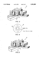
- FIG. 1 the active portion of a nonvolatile memory element 10 (i.e., the memory element without top and bottom contacts, which have been removed for clarity of illustration) according to the invention is shown.
- a hard ferromagnetic ring 12, a nonmagnetic metal ring 13, and a soft ferromagnetic ring 14 are stacked like a set of washers, and are in electrical contact.
- the hard ferromagnetic ring 12 and soft ferromagnetic ring 14 have antiparallel magnetizations ⁇ h and ⁇ s , respectively, as shown by the arrows.
- FIG. 1 the active portion of a nonvolatile memory element 10 (i.e., the memory element without top and bottom contacts, which have been removed for clarity of illustration) according to the invention is shown.
- a hard ferromagnetic ring 12, a nonmagnetic metal ring 13, and a soft ferromagnetic ring 14 are stacked like a set of washers, and are in electrical contact.
- a memory element 20 i.e., the memory element without top and bottom contacts, which have been removed for clarity of illustration
- a hard ferromagnetic ring 22, a nonmagnetic metal ring 23, and a soft ferromagnetic ring 24 are stacked like a set of washers, and are in electrical contact.
- the hard ferromagnetic ring 22 and soft ferromagnetic ring 24 have parallel magnetizations ⁇ h and ⁇ s , respectively, as shown by the arrows. If a read current J r is directed through these structures 10,20, the electrical resistance across 10 will be higher than the electrical resistance across 20, in accordance with the spin-valve effect.
- Antiferromagnetically-pinned rings will be desirable for the harder ferromagnetic layer.
- An antiferromagnetically-pinned ring will be very hard, since an antiferromagnetic pinning layer essentially fixes the direction and magnitude of the magnetic moment of the ferromagnetic layer that it contacts. With an essentially fixed magnetic moment for the harder ferromagnetic rings, a relatively hard material may be used for the softer ferromagnetic rings, to provide better ruggedness against magnetically hostile environments.
- FIG. 3 shows a memory element 30 having a plurality of interfaces which interact with spin-polarized carriers.
- the structure of memory element 30 is similar to the structure of memory element 10 shown in FIG. 1. Except where noted, analogous structures perform analogous function, and essentially the same considerations apply when selecting appropriate materials and dimensions.
- Memory element 30 includes bottom conducting lead 32.
- the upper surface of bottom conducting lead 32 supports and physically contacts the lower surface of optional layer 34 of non-magnetic material.
- the upper surface of optional antiferromagnetic ring 31, if present, is sandwiched between and physically contacts layer 34 of non-magnetic material and ring 36 of hard ferromagnetic metal.
- the lower surface of ring 36 of hard magnetic ferromagnetic metal rests on and physically contacts the upper surface of the non-magnetic layer 34. If both optional antiferromagnetic layer 31 and layer 34 of nonmagnetic material are absent, the lower surface of ring 36 rests on and physically contacts the upper surface of bottom conducting lead 32.
- Hard ferromagnetic ring 36 has a fixed magnetization that is oriented either clockwise or counterclockwise.
- non-magnetic ring 38 rests on and physically contacts the upper surface of hard ferromagnetic ring 36 and serves as the intervening, non-magnetic layer required for the spin-valve effect.
- the upper surface of non-magnetic ring 36 supports and physically contacts the soft ferromagnetic ring 39.
- the bottom surface of top conducting lead 35 rests on and physically contacts the upper surface of optional layer 37 of conducting non-magnetic material. If optional layer 37 is absent, the bottom surface of top conducting lead 35 rests upon and physically contacts the upper surface of ferromagnetic ring 39. As shown in FIG. 3, the magnetizations of ferromagnetic rings 34,38 are antiparallel, and therefore the element is in a high resistance state.
- the direction of the magnetization of ring 39 is reversible.
- Various embodiments of the invention will use various means for reversing the magnetization of ring 39, and thereby storing a data bit.
- the magnetization of ring 39 will be effected by directing a writing current J w pulse near or through ring 39. This writing current pulse may use the same or a different conductive pathway than that of a read current J r .
- a multilayered memory element includes alternating rings of hard magnetic and soft magnetic materials spaced from each other by intervening layers of nonmagnetic conductive material.
- FIG. 6 the active portion of a multilayer nonvolatile memory element 60 (i.e., the memory element without the top and bottom contacts, which have been removed for clarity of illustration) according to the invention is shown.
- Active portion 60 includes bottom nonmagnetic conducting layer 61.
- Active portion 60 includes top nonmagnetic conducting layer 63.
- Between the bottom nonmagnetic conducting layer 61 and the top nonmagnetic conducting layer 63 are a plurality of hard magnetic or antiferromagnetically-pinned rings 64, alternating with soft magnetic rings 66.
- the hard magnetic or antiferromagnetically-pinned rings 64 and soft magnetic rings 66 are separated by intervening nonmagnetic conductive rings 62, so that the structure 60 forms a conductive stack.
- the hard magnetic or antiferromagnetically-pinned rings 64 and soft magnetic rings 66 may have alternating magnetizations, thus creating a high resistance across the device 60. As shown in FIG. 7, the hard magnetic or antiferromagnetically-pinned rings 64 and soft magnetic rings 66 may have aligned magnetizations, thus creating a low resistance across the device 60.
- a non-volatile random access memory element according to the present invention will be uniform and perpendicular to the ferromagnetic rings.
- No central core of magnetic or conductive material is required for any of the above-described embodiments of the present invention.
- the core of an element according to the invention will be a dielectric. This dielectric core will help confine the read and write currents to the ferromagnetic rings and the nonmagnetic conductive rings, as is preferred.
- this dielectric core may also simplify manufacture of the preferred solid planar end nonmagnetic conducting layers.
- an embodiment of a non-volatile random access memory element according to the present invention 80 will include a diode 83.
- This diode 83 may be interposed between the bottom conducting lead 82 and the lower surface of layer 84 of non-magnetic material.
- the diode alternatively may be disposed between the top conducting lead 85 and the upper surface of layer 87 of non-magnetic material.
- the diode alternatively may be disposed between two adjacent structures in the element 80.
- Embodiments of the non-volatile random access memory element according to the present invention which incorporate a diode will generally include a separate writing circuit for applying writing current J w , so that J w can flow in two directions.
- a separate writing circuit for applying writing current J w , so that J w can flow in two directions.
- Separate reading and writing circuits permit each to be optimized. Separate reading and writing circuits permit simultaneous reading and writing of elements in an array, permitting faster operation.
- Such an embodiment can be integrated more readily into an x-y bit array. Field distribution in memory elements may be more uniform during a writing step.
- memory element 900 includes bottom conducting lead 902.
- the upper surface of bottom conducting lead 902 supports and physically contacts the lower surface of optional ring 904 of non-magnetic material, if present.
- the upper surface of optional antiferromagnetic ring 901, if present, is sandwiched between and physically contacts layer 904 of non-magnetic material and ring 906 of hard ferromagnetic metal.
- the lower surface of ring 906 of hard magnetic ferromagnetic metal rests on and physically contacts the upper surface of bottom conducting lead 902.
- the lower surface of ring 906 of hard magnetic ferromagnetic metal rests on and physically contacts the upper surface of nonmagnetic material 904.
- Hard ferromagnetic ring 906 has a fixed magnetization that is oriented either clockwise or counterclockwise.
- non-magnetic ring 908 rests on and physically contacts the upper surface of hard ferromagnetic ring 906 and serves as the intervening, non-magnetic layer required for the spin-valve effect.
- the upper surface of non-magnetic ring 906 supports and physically contacts the soft ferromagnetic ring 909.
- the bottom surface of top conducting lead 905 also rests upon and physically contacts the upper surface of soft ferromagnetic ring 909.
- ring 907 of conducting, non-magnetic material may be interposed between and contact soft ferromagnetic ring 909 and top conducting lead 905. The position of soft ferromagnetic ring 909 may be switched with the position of hard ferromagnetic ring 906 (and any antiferromagnetic pinning ring).
- Top conducting lead 905 includes a pass-though 918.
- Writing conductor 912 is positioned axially with respect to rings 904,901,906,908,909,907, and goes through pass-through 918.
- Writing conductor 912 electrically connects with top writing conducting lead 914 with bottom conducting lead 902.
- a separate bottom writing conducting lead may be employed.
- Dielectric 916 maintains proper electrical isolation.
- Writing is effected by directing writing current J w through writing conductor 912. As shown in FIG. 10, it is believed that directing current through writing conductor 912 (out of the drawing sheet in FIG. 10), a domain wall is formed at the inner perimeter of the soft magnetic ring 909, and this domain wall rapidly moves to the outer diameter of the soft magnetic ring 909, as indicated by the arrows, thus reversing the magnetization of soft magnetic ring 909.
- the ferromagnetic rings have thicknesses of about 10 ⁇ to about 100 ⁇ . More preferably, the ferromagnetic rings have thicknesses of about 50 ⁇ to about 100 ⁇ .
- the nonmagnetic conductive layers and rings have thicknesses of about 10 ⁇ to about 100 ⁇ . More preferably, the nonmagnetic conductive layers and rings have thicknesses of about 50 ⁇ to about 100 ⁇ .
- the ferromagnetic rings are Fe, Co, or Ni.
- the hard ferromagnetic rings are selected from the alloys described in U.S. Pat. No. 4,402,770 to Norman C. Koon.
- the soft magnetic alloys are selected from the alloys described in U.S. Pat. No. 4,402,043, to Norman C. Koon.
- the ferromagnetic rings having fixed magnetic state are antiferromagnetically pinned.
- a hard or antiferromagnetically-pinned ferromagnetic ring has a coercive field of at least 100 Oe and a softer ferromagnetic ring has a coercive field of less than 100 Oe.
- a writing field generated by a writing current J w will be at least the coercive field of a softer ferromagnetic ring, but less than the coercive field of a hard or antiferromagnetically-pinned ferromagnetic ring.
- a reading field generated by a reading current J r will be less than the coercive field of a softer ferromagnetic ring.
- an antiferromagnetic pinning layer comprises a metal oxide such as an iron oxide.
- the antiferromagnetic pinning layer comprises Cr or Mn, such as alloys of Cr or Mn, such as FeMn.
- the ferromagnetic rings are poled so that the easy axis of their magnetic moments are oriented to be either clockwise or counterclockwise with respect to the rings.
- the nonmagnetic layer is a ring.
- the nonmagnetic layer comprises Cu, Au, Pt, or Ag.
- Arrays of memory elements including both bit arrays and word arrays, may be assembled substantially as described in the above-cited U.S. patent application Ser. No. 130,479.
- FIG. 11 shows a simplified matrix 1100 consisting of two independent arrays 1102, 1104 of parallel current carrying bars 1106 and 1108.
- arrays 1102 and 1104 are oriented about 90° to each other.
- Current carrying bars 1106 of array 1102 are above and not directly in contact with current carrying bars 1108 of array 1104.
- Current carrying bars 1106, 1108 from arrays 1102 and 1104 are connected at their intersections by the stacked memory elements 1110 sandwiched between them.
- the interrogation current to any given element comes in one end of these bars, 1106 or 1108, passes through the element and passes out through an end of the other respective contacting bar 1108 or 1106.
- FIG. 11 shows interrogation current 1112 (shown by the lines labelled "J", with the arrow pointing in the direction of current flow) entering through end 1114, flowing through a stack 1110 and exiting through end 1116 of a current carrying bar 1108 of array 1104. Resistance is measured at ends 1120, 1122 of the specified current carrying bars employed in this example that oppose ends 1114 and 1116, respectively.
- FIG. 12 shows a 5-bit word tree 1200 consisting of one underlying base bar 1202 crossed by five overlayer bars 1204 with a stacked memory element 1206 at each intersection.
- Fabrication typically will be done lithographically, substantially as described in the above-cited U.S. patent application Ser. No. 08/130,479.
- a stack of rings typically will be laid down as a stack of disks on a bottom conductor lead, and subsequently will be "drilled out” using, e.g., a focused ion beam.
- Focused ion beams which may have beamwidths of less than 400 ⁇ , are particularly useful in making stacks of rings.
- a focused ion beam is equipped with an end-point detector or equivalent device or method to prevent the focussed ion beam from penetrating a bottom conductor lead.
- Dielectric is typically laid down, and the structure planarized. After planarization, a top conductor lead is laid down.
- an axial writing conductor may be added either before the dielectric is laid down (as a lithographic step), or after the dielectric is laid down (e.g., using a focused ion beam to "drill" an axial hole for the writing conductor).
- the function of the focused ion beam may be replaced by any suitable etching process.
Landscapes
- Engineering & Computer Science (AREA)
- Computer Hardware Design (AREA)
- Semiconductor Memories (AREA)
- Mram Or Spin Memory Techniques (AREA)
Abstract
A memory element has a sandwich structure in which rings of ferromagnetic material are spaced apart by a layer of a non-magnetic conductor (which is also typically a ring). These ferromagnetic rings will have differing magnetic hardness. At least one ring will be magnetically hard or antiferromagnetically-pinned. At least one other ring will be magnetically softer than the hard or antiferromagnetically-pinned ring. The non-magnetic conductor is at least thick enough to prevent essentially all exchange coupling between the ferromagnetic rings. Conducting leads provide current to pass through the ferromagnetic rings, perpendicular to magnetic moments in the ferromagnetic rings.
Description
1. Field of the Invention
The present invention relates generally to ferromagnetic memory and more specifically to ferromagnetic memory utilizing giant magnetoresistance and spin polarization in annular memory elements.
2. Description of the Related Art
For many years, random access memory for computers was constructed from magnetic elements. This memory had the advantage of very high reliability, nonvolatility in the event of power loss and infinite lifetime under use. Since this memory was hand assembled from three-dimensional ferrite elements, it was eventually supplanted by planar arrays of semiconductor elements. Planar arrays of semiconductors can be fabricated by lithography at a much lower cost than the cost of fabricating prior art magnetic ferrite memory elements. Additionally, these semiconductor arrays are more compact and faster than prior art ferrite magnetic memory elements. Future benefits of increasingly smaller scale in semiconductor memory are now jeopardized by the concern of loss of reliability, since very small scale semiconductor elements are not electrically robust.
Non-volatile magnetic memory elements that are read by measuring resistance have been previously demonstrated by Honeywell Corporation. These systems operate on the basis of the classical anisotropic magneto-resistance phenomena, which results in resistance differences when the magnetization is oriented perpendicular versus parallel to the current. Previous work by others has shown that a 2% change in resistance is sufficient to permit the fabrication of memory arrays compatible with existing CMOS computer electronics. Unfortunately, scaling of these elements down from the current 1 μm size has proved challenging.
The carriers in devices can be identified not only as electrons and holes, but also by their spin state being "up" or "down". Just as polarized light may be easily controlled by passing it through crossed polarizers, spin polarized electron current can be created, controlled and measured by passing it between magnetic films whose relative magnetic moments can be rotated. The spin polarization manifests itself as an extra resistance in a magnetic circuit element, commonly referred to as magneto-resistance. The modern manifestation of magneto-resistance should not be confused with older observations common to semiconductors and metal in which the carriers are merely deflected by the classical Lorentz force (V×B) in the presence of a magnetic field. This modern effect is purely quantum mechanical and occurs when two ferromagnetic metals are separated by a non-magnetic conductor. When a bias voltage causes carriers to flow from one magnetic metal into the other through the intervening conductor, the spin-polarization of the carriers can play a dominant role. The carriers leaving the first ferromagnetic metal are highly polarized because they are emitted from band states which are highly polarized. The resistance which they meet in trying to enter the second ferromagnetic layer depends strongly upon the spin polarization of the states available to them. If the ferromagnetic moments of the two magnetic metals are aligned, then the spin descriptions of the states are the same in the two materials and carriers will pass freely between them. If the two moments are anti-aligned, then the states are oppositely labeled (i.e., "up" in the first ferromagnetic layer is "down" in the second ferromagnetic layer), the carriers will find that they have fewer states to enter and will experience a higher resistance. This phenomenon is now commonly referred to as the spin-valve effect. By simply measuring the resistance between two magnetic layers, one can determine if their magnetic moments are parallel or anti-parallel.
Successful application of the spin-valve effect to magnetic memory elements would preferably minimize the cancellation of the magnetization in one ferromagnetic layer by fringing fields associated with the magnetization in another ferromagnetic layer.
Accordingly, it is an object of this invention to produce an inexpensive non-volatile random access ferromagnetic memory.
It is another object of the present invention to produce a non-volatile ferromagnetic random access memory that is faster than the presently available semiconductor random access memory.
It is a further object of the present invention to produce a highly compact non-volatile random access ferromagnetic memory.
It is a further object of the present invention to produce a non-volatile random access ferromagnetic memory based on the spin-valve effect having no significant, or minimal, cancellation of the magnetization in one ferromagnetic layer by fringing fields associated with the magnetization in another ferromagnetic layer.
It is a further object of the present invention to produce a non-volatile random access ferromagnetic memory that, when incorporated into an array, will eliminate or minimize cross-talk between elements.
These and additional objects of the invention are accomplished by a non-volatile random access memory element that employs giant magnetoresistance (GMR), i.e., the spin-valve effect. The memory element has a sandwich structure in which rings of ferromagnetic material are spaced apart by a layer of a non-magnetic conductor (which is also typically a ring). These ferromagnetic rings will have differing magnetic hardness. At least one ring will be magnetically hard or antiferromagnetically-pinned. At least one other ring will be magnetically softer than the hard or antiferromagnetically-pinned ring. The non-magnetic conductor is at least thick enough to prevent essentially all exchange coupling between the ferromagnetic rings. Conducting leads provide current to pass through the ferromagnetic rings, perpendicular to magnetic moments in the ferromagnetic rings.
The memory element may have more than one hard or antiferromagnetically pinned ring, and more than one softer ferromagnetic ring. Ferromagnetic rings should be separated by nonmagnetic conductive layers, as described above. Usually, hard or antiferromagnetically pinned rings will be alternated with softer ferromagnetic rings.
A hard or antiferromagnetically-pinned ferromagnetic ring will have a fixed magnetic state, a closed magnetic circuit, whose moment is oriented either clockwise or counterclockwise around the ring. A softer ferromagnetic ring will have a closed magnetic circuit whose moment is oriented either clockwise or counterclockwise around the ring. This orientation will be reversible so that the magnetizations in the hard and soft ferromagnetic rings selectively may be either aligned or anti-aligned.
When a voltage is applied across the two ferromagnetic rings, the resistance varies depending upon whether the magnetic moments of these rings are aligned in the same direction with respect to each other. Resistance between the two layers increases when the magnetic moments of these two ferromagnetic rings are not aligned in the same direction, i.e, anti-parallel (anti-aligned). The resistance between the two rings drops when the magnetic moments of these two ferromagnetic rings are in essentially the same direction (parallel). The parallel state can be assigned a value of "0" or "1" while the antiparallel state can be assigned, respectively, a value of "1" or "0". Thus, the alignment status of each memory element according to the present invention represents a bit of information.
The bit can be altered in a memory element according to the present invention by applying a sufficiently high current through the conducting leads in order to generate a magnetic field sufficient to align, in one direction, the magnetic moment of any soft ferromagnetic ring along one of the easy directions of orientation. The direction of orientation favored by the orienting current is of course determined by the polarity of that orienting current. Once set, the bit may be read by applying a smaller current through the appropriate conducting leads and determining whether the resistance is more or less than that of a reference resistance.
A more complete appreciation of the invention will be readily obtained by reference to the following Description of the Preferred Embodiments and the accompanying drawings in which like numerals in different figures represent the same structures or elements, wherein:
FIG. 1 shows the active portion of a non-volatile random access memory element according to the present invention in a high resistance state.
FIG. 2 shows the active portion of a non-volatile random access memory element according to the present invention in a low resistance state.
FIG. 3 shows a non-volatile random access memory element according to the present invention in a high resistance state.
FIG. 4 shows a top sectional view of a non-volatile random access memory element according to the present invention during a writing step.
FIG. 5 shows a non-volatile random access memory element according to the present invention in a low resistance state.
FIG. 6 shows the active portion of a multilayer non-volatile random access memory element according to the present invention in a high resistance state.
FIG. 7 shows the active portion of a multilayer non-volatile random access memory element according to the present invention in a low resistance state.
FIG. 8 shows a non-volatile random access memory element according to the present invention with an optional diode.
FIG. 9 shows a side sectional view of a non-volatile random access memory element according to the present invention with a separate writing circuit.
FIG. 10 shows a top sectional view of a non-volatile random access memory element according to the present invention with a separate writing circuit.
FIG. 11 shows a bit array of memory elements according to the invention.
FIG. 12 shows a word array of memory elements according to the invention.
The following United States Patent Applications are incorporated herein by reference, in their entirety and for all purposes: Ser. No. 08/130,479, filed Oct. 1, 1993 by Gary A. Prinz, now U.S. Pat. No. 5,477,482 and Ser. No. 08/130,480, filed Oct. 1, 1993 by Gary A. Prinz et al., now U.S. Pat. No. 5,475,304.
Throughout the specification and the claims that follow, it should be understood the terms "upper" and "lower" are used as terms of convenience to distinguish various surfaces relative to each other. Neither "upper" nor "lower," as used in the specification and claims that follow, imply the orientation of any element with respect to the gravitational field. Likewise, the terms "clockwise" and "counterclockwise" are used as terms of convenience to distinguish rotational directions relative to each other.
Throughout the specification and the claims that follow, it should be understood the term "ring" means a closed loop. While a ring is preferably in the shape of a circular washer, other shapes (e.g., elliptical, oval, square, etc.) are permissible. Ferromagnetic rings will constitute closed magnetic circuits.
The present invention uses the spin-valve effect as the basis of a memory element. In the memory element of the present invention, the two states, parallel and anti-parallel, represent two bits, "0" and "1". Of course, each state may be arbitrarily assigned a value of "0" or "1", provided that when the parallel state is assigned a value of "0", the antiparallel state is assigned a value of "1" and when the parallel state is assigned a value of "1", the antiparallel state is assigned a value of "0". The state of the memory element may be readily interrogated by measuring the resistance.
This principle can by illustrated by reference to FIGS. 1 and 2. In FIG. 1, the active portion of a nonvolatile memory element 10 (i.e., the memory element without top and bottom contacts, which have been removed for clarity of illustration) according to the invention is shown. A hard ferromagnetic ring 12, a nonmagnetic metal ring 13, and a soft ferromagnetic ring 14 are stacked like a set of washers, and are in electrical contact. The hard ferromagnetic ring 12 and soft ferromagnetic ring 14 have antiparallel magnetizations μh and μs, respectively, as shown by the arrows. In FIG. 2, the active portion of a memory element 20 (i.e., the memory element without top and bottom contacts, which have been removed for clarity of illustration) according to the invention is shown. A hard ferromagnetic ring 22, a nonmagnetic metal ring 23, and a soft ferromagnetic ring 24 are stacked like a set of washers, and are in electrical contact. The hard ferromagnetic ring 22 and soft ferromagnetic ring 24 have parallel magnetizations μh and μs, respectively, as shown by the arrows. If a read current Jr is directed through these structures 10,20, the electrical resistance across 10 will be higher than the electrical resistance across 20, in accordance with the spin-valve effect.
Antiferromagnetically-pinned rings will be desirable for the harder ferromagnetic layer. An antiferromagnetically-pinned ring will be very hard, since an antiferromagnetic pinning layer essentially fixes the direction and magnitude of the magnetic moment of the ferromagnetic layer that it contacts. With an essentially fixed magnetic moment for the harder ferromagnetic rings, a relatively hard material may be used for the softer ferromagnetic rings, to provide better ruggedness against magnetically hostile environments.
FIG. 3 shows a memory element 30 having a plurality of interfaces which interact with spin-polarized carriers. The structure of memory element 30 is similar to the structure of memory element 10 shown in FIG. 1. Except where noted, analogous structures perform analogous function, and essentially the same considerations apply when selecting appropriate materials and dimensions. Memory element 30 includes bottom conducting lead 32. The upper surface of bottom conducting lead 32 supports and physically contacts the lower surface of optional layer 34 of non-magnetic material. The upper surface of optional antiferromagnetic ring 31, if present, is sandwiched between and physically contacts layer 34 of non-magnetic material and ring 36 of hard ferromagnetic metal.
If optional antiferromagnetic layer 31 is absent, the lower surface of ring 36 of hard magnetic ferromagnetic metal, for example, Co, rests on and physically contacts the upper surface of the non-magnetic layer 34. If both optional antiferromagnetic layer 31 and layer 34 of nonmagnetic material are absent, the lower surface of ring 36 rests on and physically contacts the upper surface of bottom conducting lead 32. Hard ferromagnetic ring 36 has a fixed magnetization that is oriented either clockwise or counterclockwise.
The lower surface of non-magnetic ring 38 rests on and physically contacts the upper surface of hard ferromagnetic ring 36 and serves as the intervening, non-magnetic layer required for the spin-valve effect. The upper surface of non-magnetic ring 36 supports and physically contacts the soft ferromagnetic ring 39. The bottom surface of top conducting lead 35 rests on and physically contacts the upper surface of optional layer 37 of conducting non-magnetic material. If optional layer 37 is absent, the bottom surface of top conducting lead 35 rests upon and physically contacts the upper surface of ferromagnetic ring 39. As shown in FIG. 3, the magnetizations of ferromagnetic rings 34,38 are antiparallel, and therefore the element is in a high resistance state.
The direction of the magnetization of ring 39 is reversible. Various embodiments of the invention will use various means for reversing the magnetization of ring 39, and thereby storing a data bit. Most typically, the magnetization of ring 39 will be effected by directing a writing current Jw pulse near or through ring 39. This writing current pulse may use the same or a different conductive pathway than that of a read current Jr.
Referring to FIG. 4, if a sufficiently large writing current Jw pulse flows from bottom conducting lead 32 to top conducting lead 35 (i.e., with reference to FIG. 4 current flow is out of the drawing sheet), this current will create a magnetic field, and the magnetization of the soft magnetic ring 39 will be reversed. Harder magnetic ring 36 (not shown) will be unaffected by Jw, due to its higher coercivity. This reversal of magnetization in ring 39 typically will be abrupt. Without wishing to be bound by theory, it is believed that as writing current Jw is applied, a domain wall is formed at the outer perimeter of the soft magnetic ring 39, and this domain wall rapidly moves to the inner diameter of the soft magnetic ring 39, as indicated by the arrows.
As shown in FIG. 5, after the application of the pulse of writing current Jw, the magnetizations of ferromagnetic rings 34,38 are parallel, and therefore the element is in a low resistance state. Reversing the direction of Jw will reverse the change to the magnetization of soft magnetic ring 39.
Because ΔR/R effects come primarily from interfacial spin scattering, it is desirable to provide memory elements having a multilayer structure, with a maximum of interfaces being forced into a length less than the spin-relaxation length. To this end, a multilayered memory element according to the present invention includes alternating rings of hard magnetic and soft magnetic materials spaced from each other by intervening layers of nonmagnetic conductive material.
In FIG. 6, the active portion of a multilayer nonvolatile memory element 60 (i.e., the memory element without the top and bottom contacts, which have been removed for clarity of illustration) according to the invention is shown. Active portion 60 includes bottom nonmagnetic conducting layer 61. Active portion 60 includes top nonmagnetic conducting layer 63. Between the bottom nonmagnetic conducting layer 61 and the top nonmagnetic conducting layer 63 are a plurality of hard magnetic or antiferromagnetically-pinned rings 64, alternating with soft magnetic rings 66. The hard magnetic or antiferromagnetically-pinned rings 64 and soft magnetic rings 66 are separated by intervening nonmagnetic conductive rings 62, so that the structure 60 forms a conductive stack. As shown in FIG. 6, the hard magnetic or antiferromagnetically-pinned rings 64 and soft magnetic rings 66 may have alternating magnetizations, thus creating a high resistance across the device 60. As shown in FIG. 7, the hard magnetic or antiferromagnetically-pinned rings 64 and soft magnetic rings 66 may have aligned magnetizations, thus creating a low resistance across the device 60.
Preferably, current flow through a non-volatile random access memory element according to the present invention will be uniform and perpendicular to the ferromagnetic rings. No central core of magnetic or conductive material is required for any of the above-described embodiments of the present invention. Frequently, the core of an element according to the invention will be a dielectric. This dielectric core will help confine the read and write currents to the ferromagnetic rings and the nonmagnetic conductive rings, as is preferred. Moreover, this dielectric core may also simplify manufacture of the preferred solid planar end nonmagnetic conducting layers.
It may be desirable for some embodiments of the present invention to have a diode in the memory element, to restrict current flow to a single direction. This is most typically advantageous if a plurality of elements are connected in an x-y bit array. To address a single element in an x-y bit array, it is typically desired to confine current flow to a single direction. However, this is not an obstacle in a word array.
As shown in FIG. 8, an embodiment of a non-volatile random access memory element according to the present invention 80 will include a diode 83. This diode 83 may be interposed between the bottom conducting lead 82 and the lower surface of layer 84 of non-magnetic material. The diode alternatively may be disposed between the top conducting lead 85 and the upper surface of layer 87 of non-magnetic material. The diode alternatively may be disposed between two adjacent structures in the element 80.
Embodiments of the non-volatile random access memory element according to the present invention which incorporate a diode will generally include a separate writing circuit for applying writing current Jw, so that Jw can flow in two directions. There are several advantages to such an embodiment. Separate reading and writing circuits permit each to be optimized. Separate reading and writing circuits permit simultaneous reading and writing of elements in an array, permitting faster operation. Such an embodiment can be integrated more readily into an x-y bit array. Field distribution in memory elements may be more uniform during a writing step.
In an embodiment of the invention, a separate circuit is provided for supplying writing current Jw. An example of such an embodiment is shown in FIGS. 9 and 10. In FIG. 9, memory element 900 includes bottom conducting lead 902. The upper surface of bottom conducting lead 902 supports and physically contacts the lower surface of optional ring 904 of non-magnetic material, if present. The upper surface of optional antiferromagnetic ring 901, if present, is sandwiched between and physically contacts layer 904 of non-magnetic material and ring 906 of hard ferromagnetic metal. If optional antiferromagnetic ring 901 and nonmagnetic material 904, are absent, the lower surface of ring 906 of hard magnetic ferromagnetic metal, for example, Co, rests on and physically contacts the upper surface of bottom conducting lead 902. Likewise, if optional antiferromagnetic ring 901 is absent, the lower surface of ring 906 of hard magnetic ferromagnetic metal rests on and physically contacts the upper surface of nonmagnetic material 904. Hard ferromagnetic ring 906 has a fixed magnetization that is oriented either clockwise or counterclockwise.
The lower surface of non-magnetic ring 908 rests on and physically contacts the upper surface of hard ferromagnetic ring 906 and serves as the intervening, non-magnetic layer required for the spin-valve effect. The upper surface of non-magnetic ring 906 supports and physically contacts the soft ferromagnetic ring 909. The bottom surface of top conducting lead 905 also rests upon and physically contacts the upper surface of soft ferromagnetic ring 909. Alternatively, ring 907 of conducting, non-magnetic material may be interposed between and contact soft ferromagnetic ring 909 and top conducting lead 905. The position of soft ferromagnetic ring 909 may be switched with the position of hard ferromagnetic ring 906 (and any antiferromagnetic pinning ring).
Top conducting lead 905 includes a pass-though 918. Writing conductor 912 is positioned axially with respect to rings 904,901,906,908,909,907, and goes through pass-through 918. Writing conductor 912 electrically connects with top writing conducting lead 914 with bottom conducting lead 902. Alternatively, a separate bottom writing conducting lead may be employed. Dielectric 916 maintains proper electrical isolation.
Writing is effected by directing writing current Jw through writing conductor 912. As shown in FIG. 10, it is believed that directing current through writing conductor 912 (out of the drawing sheet in FIG. 10), a domain wall is formed at the inner perimeter of the soft magnetic ring 909, and this domain wall rapidly moves to the outer diameter of the soft magnetic ring 909, as indicated by the arrows, thus reversing the magnetization of soft magnetic ring 909.
Preferably, the ferromagnetic rings have thicknesses of about 10 Å to about 100 Å. More preferably, the ferromagnetic rings have thicknesses of about 50 Å to about 100 Å. Preferably, the nonmagnetic conductive layers and rings have thicknesses of about 10 Å to about 100 Å. More preferably, the nonmagnetic conductive layers and rings have thicknesses of about 50 Å to about 100 Å.
Typically the ferromagnetic rings are Fe, Co, or Ni. Typically, the hard ferromagnetic rings are selected from the alloys described in U.S. Pat. No. 4,402,770 to Norman C. Koon. Typically, the soft magnetic alloys are selected from the alloys described in U.S. Pat. No. 4,402,043, to Norman C. Koon. Typically, the ferromagnetic rings having fixed magnetic state are antiferromagnetically pinned. Typically, a hard or antiferromagnetically-pinned ferromagnetic ring has a coercive field of at least 100 Oe and a softer ferromagnetic ring has a coercive field of less than 100 Oe.
A writing field generated by a writing current Jw will be at least the coercive field of a softer ferromagnetic ring, but less than the coercive field of a hard or antiferromagnetically-pinned ferromagnetic ring. A reading field generated by a reading current Jr will be less than the coercive field of a softer ferromagnetic ring.
Typically, an antiferromagnetic pinning layer comprises a metal oxide such as an iron oxide. Typically, the antiferromagnetic pinning layer comprises Cr or Mn, such as alloys of Cr or Mn, such as FeMn. Preferably, the ferromagnetic rings (especially soft ferromagnetic rings) are poled so that the easy axis of their magnetic moments are oriented to be either clockwise or counterclockwise with respect to the rings.
Typically, the nonmagnetic layer is a ring. Typically, the nonmagnetic layer comprises Cu, Au, Pt, or Ag.
Arrays of memory elements, including both bit arrays and word arrays, may be assembled substantially as described in the above-cited U.S. patent application Ser. No. 130,479.
FIG. 11 shows a simplified matrix 1100 consisting of two independent arrays 1102, 1104 of parallel current carrying bars 1106 and 1108. Preferably, arrays 1102 and 1104 are oriented about 90° to each other. Current carrying bars 1106 of array 1102 are above and not directly in contact with current carrying bars 1108 of array 1104. Current carrying bars 1106, 1108 from arrays 1102 and 1104 are connected at their intersections by the stacked memory elements 1110 sandwiched between them. The interrogation current to any given element comes in one end of these bars, 1106 or 1108, passes through the element and passes out through an end of the other respective contacting bar 1108 or 1106. The other ends of bars 1106 and 1108 provide the leads for measurement of the potential drop, thus providing a true 4-point probe measurement which eliminates the lead resistance in the circuit. For purposes of illustration only, FIG. 11 shows interrogation current 1112 (shown by the lines labelled "J", with the arrow pointing in the direction of current flow) entering through end 1114, flowing through a stack 1110 and exiting through end 1116 of a current carrying bar 1108 of array 1104. Resistance is measured at ends 1120, 1122 of the specified current carrying bars employed in this example that oppose ends 1114 and 1116, respectively.
In order for the x-y matrix of FIG. 11 to give true measurements of a single element, parallel paths of conduction must be eliminated. This goal is accomplished by providing diode film elements 1122 at one end of the stack where contact to the bars are made, either above or below the current bar through which the current enters the stack. This arrangement will prevent any competing currents since all currents are now forced to pass one way through the elements.
FIG. 12 shows a 5-bit word tree 1200 consisting of one underlying base bar 1202 crossed by five overlayer bars 1204 with a stacked memory element 1206 at each intersection.
Fabrication typically will be done lithographically, substantially as described in the above-cited U.S. patent application Ser. No. 08/130,479. A stack of rings typically will be laid down as a stack of disks on a bottom conductor lead, and subsequently will be "drilled out" using, e.g., a focused ion beam. Focused ion beams, which may have beamwidths of less than 400 Å, are particularly useful in making stacks of rings. Preferably, a focused ion beam is equipped with an end-point detector or equivalent device or method to prevent the focussed ion beam from penetrating a bottom conductor lead. Dielectric is typically laid down, and the structure planarized. After planarization, a top conductor lead is laid down.
In an embodiment where a memory element includes a separate writing circuit, an axial writing conductor may be added either before the dielectric is laid down (as a lithographic step), or after the dielectric is laid down (e.g., using a focused ion beam to "drill" an axial hole for the writing conductor).
The function of the focused ion beam may be replaced by any suitable etching process.
Obviously, many modifications and variations of the present invention are possible in light of the above teachings. It is therefore to be understood that, within the scope of the appended claims, the invention may be practiced otherwise than as specifically described.
Claims (21)
1. A non-volatile ferromagnetic random access memory element comprising:
a first ferromagnetic ring and a second ferromagnetic ring, wherein one of said ferromagnetic rings is hard or antiferromagnetically-pinned and the other ferromagnetic ring is magnetically softer than said hard or antiferromagnetically-pinned ring;
a non-magnetic conductive layer sandwiched between and contacting said first and second ferromagnetic rings, for preventing essentially all exchange coupling between said first and second ferromagnetic rings;
a first end nonmagnetic conducting layer at one end of said ferromagnetic random access memory element;
a second end nonmagnetic conducting layer at an opposite end of said non-volatile ferromagnetic random access memory element;
said first and second end conducting layers defining a conductive path for flowing a current from said first ferromagnetic ring, through said nonmagnetic conductive layer, to said second ferromagnetic ring, said conductive path being perpendicular to a magnetic moment of at least one of said first and second ferromagnetic rings.
2. The non-volatile ferromagnetic random access memory element of claim 1, wherein said first and second ferromagnetic rings, and said nonmagnetic conductive layer, each have thicknesses of about 10 Å to about 100 Å.
3. The non-volatile ferromagnetic random access memory element of claim 2, wherein said first and second ferromagnetic rings, and said nonmagnetic conductive layer, each have thicknesses of about 50 Å to about 100 Å.
4. The non-volatile ferromagnetic random access memory element of claim 1, wherein said first and second ferromagnetic rings comprise Fe, Co or Ni.
5. The non-volatile ferromagnetic random access memory element of claim 1, wherein said nonmagnetic conductive layer comprises Cu, Pt, Ag or Au.
6. The non-volatile ferromagnetic random access memory element of claim 1, wherein said ferromagnetic rings are poled so that the easy axes of the magnetic moments of said rings are oriented to be either clockwise or counterclockwise with respect to said rings.
7. The non-volatile ferromagnetic random access memory element of claim 1, wherein said hard or antiferromagnetically-pinned ferromagnetic ring has a fixed magnetization forming a closed magnetic circuit about said hard or antiferromagnetically-pinned ferromagnetic ring, and said softer ferromagnetic ring has a magnetization forming a closed magnetic circuit about said softer ferromagnetic ring, said magnetization of said softer ferromagnetic ring being reversible upon the application of a writing current flow between said first end nonmagnetic conducting layer and said second end nonmagnetic conducting layer.
8. The non-volatile ferromagnetic random access memory element of claim 1, wherein said first end nonmagnetic conducting layer and said second end nonmagnetic conducting layer are solid planar layers.
9. The non-volatile ferromagnetic random access memory element of claim 1, wherein said first ferromagnetic ring has an upper surface and a lower surface, and further comprising:
an antiferromagnetic layer between said first ferromagnetic ring and said first end conducting layer, said antiferromagnetic layer having an upper and a lower surface, said upper surface of said antiferromagnetic layer physically contacting said lower surface of said first ferromagnetic ring, said antiferromagnetic layer pinning, by exchange coupling with said first ferromagnetic ring, the orientation of a closed magnetic circuit within the plane of said first ferromagnetic ring.
10. The non-volatile ferromagnetic memory element of claim 9, wherein said antiferromagnetic layer comprises Cr, Mn, a metal oxide, or combinations thereof.
11. The non-volatile ferromagnetic memory element of claim 9, wherein said antiferromagnetic layer comprises FeMn.
12. The non-volatile ferromagnetic memory element of claim 9, wherein said antiferromagnetic layer comprises an oxide of iron.
13. The non-volatile ferromagnetic random access memory element of claim 1, wherein said nonmagnetic conductive layer is a ring.
14. An array of non-volatile ferromagnetic random access memory elements, comprising:
a first row of at least two non-volatile ferromagnetic random access memory elements;
each of said non-volatile ferromagnetic random access memory elements having upper and lower surfaces and including:
(i) a first ferromagnetic ring and a second ferromagnetic ring, wherein one of said ferromagnetic rings is hard or antiferromagnetically-pinned and the other ferromagnetic ring is magnetically softer than said hard or antiferromagnetically-pinned ring;
(ii) a non-magnetic conductive layer sandwiched between said first and second ferromagnetic rings;
a first conducting lead extending across and physically contacting said upper surfaces of each of said at least two non-volatile ferromagnetic random access memory elements in said first row;
a second conducting lead, transverse to, but not contacting, said first conducting lead, extending across and physically contacting only a first one of said at least two non-volatile ferromagnetic random access memory elements in said first row at said lower surface of said first one of said ferromagnetic random access memory elements in said first row, said first and second conducting leads defining a conductive path for flowing a current from said first magnetic layer, through said nonmagnetic metallic layer, to said second magnetic layer, said conductive path being perpendicular to closed magnetic currents in said ferromagnetic rings.
15. The array of claim 14, further comprising a third conducting lead, transverse to, but not contacting, said first conducting lead, extending across and physically contacting only a second one of said at least two non-volatile ferromagnetic random access memory elements at said lower surface of said second one of said non-volatile ferromagnetic random access memory elements in said first row.
16. The array of claim 15, further comprising:
a second row of at least two non-volatile ferromagnetic random access memory elements;
a fourth conducting lead extending across and physically contacting said upper surfaces of said at least two non-volatile ferromagnetic random access memory elements in said second row, but not physically contacting said at least two non-volatile ferromagnetic random access memory elements in said first row;
said second conducting lead extending across and physically contacting only a first one of said at least two non-volatile ferromagnetic random access memory elements in said second row at said lower surface of said ferromagnetic random access memory element in said second row;
said third conducting lead extending across and physically contacting only a second one of said at least two non-volatile ferromagnetic random access memory elements in said second row at said lower surface of said second one of said ferromagnetic random access memory elements in said second row.
17. The array of claim 16, wherein said first and fourth conducting leads are parallel to each other, said second and third conducting leads are parallel to each other, and said first, second, third and fourth conducting leads collectively define a grid.
18. The array of claim 17, wherein said first and fourth conducting leads extend essentially perpendicular to said second and third conducting leads.
19. The non-volatile ferromagnetic random access memory element of claim 1, wherein said hard or antiferromagnetically-pinned ferromagnetic layer has a coercive field of at least 100 Oe and said softer ferromagnetic layer has a coercive field of less than 100 Oe.
20. A method of storing digital data, comprising the steps of:
setting a bit of data as either a "0" or "1" in a non-volatile ferromagnetic random access memory element including:
a first ferromagnetic ring and a second ferromagnetic ring, wherein one of said ferromagnetic rings is hard or antiferromagnetically-pinned and the other ferromagnetic ring is magnetically softer than said hard or antiferromagnetically-pinned ring, and said ferromagnetic rings are poled so that the easy axes of the magnetic moments of said rings are oriented to be either clockwise or counterclockwise with respect to said rings and have magnetizations forming closed magnetic circuits about said rings;
a nonmagnetic conducting layer sandwiched between said first and second ferromagnetic rings;
a first end nonmagnetic conducting layer at one end of said non-volatile ferromagnetic random access memory element; and
a second end nonmagnetic conducting layer at an opposite end of said non-volatile ferromagnetic random access memory element;
by exposing said non-volatile ferromagnetic random access memory element to magnetic field which sets said magnetic moment of said softer ferromagnetic ring to be either parallel or antiparallel to said magnetic moment of said hard or antiferromagnetically-pinned ferromagnetic ring, wherein resistance across said non-volatile ferromagnetic random access memory element after the application of said field is set as a "0" or "1".
21. The method of storing digital data of claim 20, wherein said exposing said non-volatile ferromagnetic random access memory element to magnetic field is effected by directing current through said first and second end conducting layers, said first ferromagnetic ring, said nonmagnetic conductive layer, and said second ferromagnetic ring, wherein said current flows essentially parallel to the axis of said rings.
Priority Applications (1)
| Application Number | Priority Date | Filing Date | Title |
|---|---|---|---|
| US08/391,971 US5541868A (en) | 1995-02-21 | 1995-02-21 | Annular GMR-based memory element |
Applications Claiming Priority (1)
| Application Number | Priority Date | Filing Date | Title |
|---|---|---|---|
| US08/391,971 US5541868A (en) | 1995-02-21 | 1995-02-21 | Annular GMR-based memory element |
Publications (1)
| Publication Number | Publication Date |
|---|---|
| US5541868A true US5541868A (en) | 1996-07-30 |
Family
ID=23548733
Family Applications (1)
| Application Number | Title | Priority Date | Filing Date |
|---|---|---|---|
| US08/391,971 Expired - Lifetime US5541868A (en) | 1995-02-21 | 1995-02-21 | Annular GMR-based memory element |
Country Status (1)
| Country | Link |
|---|---|
| US (1) | US5541868A (en) |
Cited By (150)
| Publication number | Priority date | Publication date | Assignee | Title |
|---|---|---|---|---|
| US5745406A (en) * | 1995-11-13 | 1998-04-28 | Oki Electric Industry Co., Ltd. | High-speed, low-current magnetoresistive memory device |
| US5856008A (en) * | 1997-06-05 | 1999-01-05 | Lucent Technologies Inc. | Article comprising magnetoresistive material |
| US5919580A (en) * | 1997-05-22 | 1999-07-06 | University Of Alabama | Spin valve device containing a Cr-rich antiferromagnetic pinning layer |
| US5923504A (en) * | 1995-09-21 | 1999-07-13 | Tdk Corporation | Magnetoresistance device |
| US5966012A (en) * | 1997-10-07 | 1999-10-12 | International Business Machines Corporation | Magnetic tunnel junction device with improved fixed and free ferromagnetic layers |
| US5969978A (en) * | 1998-09-30 | 1999-10-19 | The United States Of America As Represented By The Secretary Of The Navy | Read/write memory architecture employing closed ring elements |
| EP0910092A3 (en) * | 1997-09-18 | 1999-12-29 | Canon Kabushiki Kaisha | Magnetic thin film memory element and recording/reproduction method using such memory element |
| WO2000004551A1 (en) * | 1998-07-20 | 2000-01-27 | Motorola, Inc. | Mram with shared word and digit lines |
| WO2000042614A1 (en) * | 1999-01-13 | 2000-07-20 | Infineon Technologies Ag | Read/write architecture for a mram |
| WO2000052771A1 (en) * | 1999-02-26 | 2000-09-08 | Infineon Technologies Ag | Storage cell arrangement and method for producing the same |
| US6130814A (en) * | 1998-07-28 | 2000-10-10 | International Business Machines Corporation | Current-induced magnetic switching device and memory including the same |
| US6171693B1 (en) | 1998-10-27 | 2001-01-09 | The United States Of America As Represented By The Secretary Of The Navy | Structures with improved magnetic characteristics for giant magneto-resistance applications |
| US6269018B1 (en) | 2000-04-13 | 2001-07-31 | International Business Machines Corporation | Magnetic random access memory using current through MTJ write mechanism |
| WO2001057506A1 (en) * | 2000-02-04 | 2001-08-09 | The United States Of America As Represented By The Secretary Of The Navy | High efficiency magnetic sensor for magnetic particles |
| US6331944B1 (en) | 2000-04-13 | 2001-12-18 | International Business Machines Corporation | Magnetic random access memory using a series tunnel element select mechanism |
| US6391483B1 (en) | 1999-03-30 | 2002-05-21 | Carnegie Mellon University | Magnetic device and method of forming same |
| FR2817999A1 (en) * | 2000-12-07 | 2002-06-14 | Commissariat Energie Atomique | Magnetic device with polarisation of spin incorporating a three-layer stack with two magnetic layers separated by a non-magnetic conducting layer for the realisation of magnetic memory |
| US6495873B2 (en) | 1998-09-07 | 2002-12-17 | Infineon Technologies Ag | Magnetoresistive element and use thereof as a memory element in a memory cell configuration |
| FR2828001A1 (en) * | 2001-07-27 | 2003-01-31 | Thales Sa | Magnetic random access memory magnetic switching command having electrode planes/ferromagnetic layer thickness lower than first and electrode thickness allowing magnetic coupling. |
| US6515897B1 (en) | 2000-04-13 | 2003-02-04 | International Business Machines Corporation | Magnetic random access memory using a non-linear memory element select mechanism |
| US20030048676A1 (en) * | 2001-08-31 | 2003-03-13 | Nve Corporation | Antiparallel magnetoresistive memory cells |
| US6538921B2 (en) | 2000-08-17 | 2003-03-25 | Nve Corporation | Circuit selection of magnetic memory cells and related cell structures |
| US6552554B1 (en) * | 2001-12-06 | 2003-04-22 | The United States Of America As Represented By The Secretary Of The Navy | Testing current perpendicular to plane giant magnetoresistance multilayer devices |
| US6577526B1 (en) | 1998-08-12 | 2003-06-10 | Infineon Technologies Ag | Magnetoresistive element and the use thereof as storage element in a storage cell array |
| US6624490B2 (en) | 2000-10-26 | 2003-09-23 | The University Of Iowa Research Foundation | Unipolar spin diode and the applications of the same |
| WO2003067600A3 (en) * | 2002-02-06 | 2003-11-13 | Micron Technology Inc | Antiferromagnetically stabilized pseudo spin valve for memory applications |
| WO2003098637A1 (en) * | 2002-05-22 | 2003-11-27 | Koninklijke Philips Electronics N.V. | Mram-cell and array-architecture with maximum read-out signal and reduced electromagnetic interference |
| US20040001368A1 (en) * | 2002-05-16 | 2004-01-01 | Nova Research, Inc. | Methods of fabricating magnetoresistive memory devices |
| US6674664B2 (en) | 2001-05-07 | 2004-01-06 | Nve Corporation | Circuit selected joint magnetoresistive junction tunneling-giant magnetoresistive effects memory cells |
| US20040032765A1 (en) * | 2002-08-13 | 2004-02-19 | Micron Technology, Inc. | Closed flux magnetic memory |
| US20040042248A1 (en) * | 2002-08-30 | 2004-03-04 | Manish Sharma | Magnetic memory cell having an annular data layer and a soft reference layer |
| US20040043562A1 (en) * | 2002-08-30 | 2004-03-04 | Manish Sharma | Magnetic memory cell having an annular data layer and a soft reference layer |
| US20040094785A1 (en) * | 2002-11-18 | 2004-05-20 | Xiaochun Zhu | Magentic memory element and memory device including same |
| US6739132B2 (en) | 2002-04-30 | 2004-05-25 | Adc Telecommunications, Inc. | Thermal micro-actuator based on selective electrical excitation |
| US20040211996A1 (en) * | 2003-02-10 | 2004-10-28 | Ross Caroline A. | Magnetic memory elements using 360 degree walls |
| US20040213039A1 (en) * | 2003-04-23 | 2004-10-28 | Keio University | Magnetic ring unit and magnetic memory device |
| US20040228171A1 (en) * | 2003-05-14 | 2004-11-18 | Macronix International Co., Ltd. | Bistable magnetic device using soft magnetic intermediary material |
| US20040233761A1 (en) * | 1998-10-30 | 2004-11-25 | Schwabe Nikolai Franz Gregoe | Magnetic storage device |
| US6829159B2 (en) * | 2000-08-31 | 2004-12-07 | Canon Kabushiki Kaisha | Magnetic device |
| WO2004038725A3 (en) * | 2002-10-22 | 2005-05-06 | Btg Int Ltd | Magnetic memory device |
| US20050158881A1 (en) * | 2004-01-15 | 2005-07-21 | Manish Sharma | Method of making toroidal mram cells |
| US6956763B2 (en) | 2003-06-27 | 2005-10-18 | Freescale Semiconductor, Inc. | MRAM element and methods for writing the MRAM element |
| US6967366B2 (en) | 2003-08-25 | 2005-11-22 | Freescale Semiconductor, Inc. | Magnetoresistive random access memory with reduced switching field variation |
| US20060007728A1 (en) * | 2004-06-21 | 2006-01-12 | Honeywell International Inc. | Nonvolatile memory vertical ring bit and write-read structure |
| US20060215443A1 (en) * | 2005-03-23 | 2006-09-28 | Honeywell International Inc. | Architectures for cpp ring shaped (rs) devices |
| US7129098B2 (en) | 2004-11-24 | 2006-10-31 | Freescale Semiconductor, Inc. | Reduced power magnetoresistive random access memory elements |
| US20070030728A1 (en) * | 2003-08-19 | 2007-02-08 | New York University | High speed low power annular magnetic devices based on current induced spin-momentum transfer |
| US7184300B2 (en) | 2001-10-16 | 2007-02-27 | Freescale Semiconductor, Inc. | Magneto resistance random access memory element |
| US20070090903A1 (en) * | 2005-10-24 | 2007-04-26 | Seagate Technology Llc | Rotating write field generated by circulating domain walls in a magnetic ring: a DC-driven high-frequency oscillator |
| WO2007076718A1 (en) * | 2005-12-31 | 2007-07-12 | Institute Of Physics, Chinese Academy Of Sciences | A close shaped magnetic multi-layer film comprising or not comprising a metal core and the manufacture method and the application of the same |
| CN1326648C (en) * | 2001-06-13 | 2007-07-18 | 赫加奈斯公司 | Method for preparing high-density soft magnetic products |
| US20070236978A1 (en) * | 2006-04-06 | 2007-10-11 | Wilson Jannier M R | Non-volatile Reactive Magnetic Memory device (REMM) |
| US20070279971A1 (en) * | 2004-06-04 | 2007-12-06 | Micron Technology, Inc. | Modified pseudo-spin valve (psv) for memory applications |
| US20080074224A1 (en) * | 2006-09-25 | 2008-03-27 | Castano Fernando J | Wheatstone-bridge magnetoresistive device |
| US20080112094A1 (en) * | 2003-08-19 | 2008-05-15 | New York University | High speed low power annular magnetic devices based on current induced spin-momentum transfer |
| US7447061B1 (en) | 2007-03-02 | 2008-11-04 | The United States Of America As Represented By The Secretary Of The Navy | Magnetoresistive memory array circuit |
| US7465589B2 (en) | 2002-07-17 | 2008-12-16 | Everspin Technologies, Inc. | Multi-state magnetoresistance random access cell with improved memory storage density |
| CN100477316C (en) * | 2006-04-11 | 2009-04-08 | 中国科学院物理研究所 | Magnetic Logic Element Based on Ring Closed Magnetic Multilayer Film |
| CN100476995C (en) * | 2006-01-11 | 2009-04-08 | 中国科学院物理研究所 | Magnetic random access storage based on closed magnetic multilayer film and control method thereof |
| US20090296462A1 (en) * | 2003-08-19 | 2009-12-03 | New York University | High speed low power magnetic devices based on current induced spin-momentum transfer |
| CN100576343C (en) * | 2002-02-06 | 2009-12-30 | 美光科技公司 | Antiferromagnetically stable pseudo-spintronic tube for memory |
| CN101315948B (en) * | 2007-05-29 | 2010-05-26 | 中国科学院物理研究所 | a spin transistor |
| CN101221849B (en) * | 2007-01-09 | 2011-04-06 | 中国科学院物理研究所 | Magnetic multilayer film with geometrical shape and preparation method and application thereof |
| CN1992105B (en) * | 2005-12-31 | 2011-05-04 | 中国科学院物理研究所 | Ring-shaped magnetic multi-layer film having metallic core and method for making same and use |
| US20110241138A1 (en) * | 2010-03-31 | 2011-10-06 | Chun-I Hsieh | Magnetoresistive random access memory element and fabrication method thereof |
| US8063393B2 (en) | 2008-01-30 | 2011-11-22 | Industrial Technology Research Institute | Memory devices, stylus-shaped structures, electronic apparatuses, and methods for fabricating the same |
| CN101847436B (en) * | 2009-03-24 | 2012-09-05 | 中国科学院物理研究所 | Magnetic multilayer film random memorizer based on vertical transistor |
| US20120241828A1 (en) * | 2011-03-24 | 2012-09-27 | Seung Hyun Lee | Semiconductor memory device and manufacturing method thereof |
| US8755222B2 (en) | 2003-08-19 | 2014-06-17 | New York University | Bipolar spin-transfer switching |
| US20150023092A1 (en) * | 2013-07-17 | 2015-01-22 | National Yunlin University Of Science And Technology | Ring-shaped magnetoresistive memory device and writing method thereof |
| DE10305823B4 (en) * | 2002-02-15 | 2015-03-05 | Dexerials Corp. | Magnetoresistance effect element and magnetic memory with such |
| US8982613B2 (en) | 2013-06-17 | 2015-03-17 | New York University | Scalable orthogonal spin transfer magnetic random access memory devices with reduced write error rates |
| US9082888B2 (en) | 2012-10-17 | 2015-07-14 | New York University | Inverted orthogonal spin transfer layer stack |
| US9082950B2 (en) | 2012-10-17 | 2015-07-14 | New York University | Increased magnetoresistance in an inverted orthogonal spin transfer layer stack |
| CN105206741A (en) * | 2014-06-23 | 2015-12-30 | 中芯国际集成电路制造(上海)有限公司 | Magnetic tunnel junction unit and method for preparing same |
| US9263667B1 (en) | 2014-07-25 | 2016-02-16 | Spin Transfer Technologies, Inc. | Method for manufacturing MTJ memory device |
| US9337412B2 (en) | 2014-09-22 | 2016-05-10 | Spin Transfer Technologies, Inc. | Magnetic tunnel junction structure for MRAM device |
| US9728712B2 (en) | 2015-04-21 | 2017-08-08 | Spin Transfer Technologies, Inc. | Spin transfer torque structure for MRAM devices having a spin current injection capping layer |
| US9741926B1 (en) | 2016-01-28 | 2017-08-22 | Spin Transfer Technologies, Inc. | Memory cell having magnetic tunnel junction and thermal stability enhancement layer |
| US9773974B2 (en) | 2015-07-30 | 2017-09-26 | Spin Transfer Technologies, Inc. | Polishing stop layer(s) for processing arrays of semiconductor elements |
| US9812184B2 (en) | 2007-10-31 | 2017-11-07 | New York University | Current induced spin-momentum transfer stack with dual insulating layers |
| US9853206B2 (en) | 2015-06-16 | 2017-12-26 | Spin Transfer Technologies, Inc. | Precessional spin current structure for MRAM |
| US10032978B1 (en) | 2017-06-27 | 2018-07-24 | Spin Transfer Technologies, Inc. | MRAM with reduced stray magnetic fields |
| US10141499B1 (en) | 2017-12-30 | 2018-11-27 | Spin Transfer Technologies, Inc. | Perpendicular magnetic tunnel junction device with offset precessional spin current layer |
| US10163479B2 (en) | 2015-08-14 | 2018-12-25 | Spin Transfer Technologies, Inc. | Method and apparatus for bipolar memory write-verify |
| US10199083B1 (en) | 2017-12-29 | 2019-02-05 | Spin Transfer Technologies, Inc. | Three-terminal MRAM with ac write-assist for low read disturb |
| US10229724B1 (en) | 2017-12-30 | 2019-03-12 | Spin Memory, Inc. | Microwave write-assist in series-interconnected orthogonal STT-MRAM devices |
| US10236439B1 (en) | 2017-12-30 | 2019-03-19 | Spin Memory, Inc. | Switching and stability control for perpendicular magnetic tunnel junction device |
| US10236048B1 (en) | 2017-12-29 | 2019-03-19 | Spin Memory, Inc. | AC current write-assist in orthogonal STT-MRAM |
| US10236047B1 (en) | 2017-12-29 | 2019-03-19 | Spin Memory, Inc. | Shared oscillator (STNO) for MRAM array write-assist in orthogonal STT-MRAM |
| US10255962B1 (en) | 2017-12-30 | 2019-04-09 | Spin Memory, Inc. | Microwave write-assist in orthogonal STT-MRAM |
| US10270027B1 (en) | 2017-12-29 | 2019-04-23 | Spin Memory, Inc. | Self-generating AC current assist in orthogonal STT-MRAM |
| US10319900B1 (en) | 2017-12-30 | 2019-06-11 | Spin Memory, Inc. | Perpendicular magnetic tunnel junction device with precessional spin current layer having a modulated moment density |
| US10339993B1 (en) | 2017-12-30 | 2019-07-02 | Spin Memory, Inc. | Perpendicular magnetic tunnel junction device with skyrmionic assist layers for free layer switching |
| US10360964B2 (en) | 2016-09-27 | 2019-07-23 | Spin Memory, Inc. | Method of writing contents in memory during a power up sequence using a dynamic redundancy register in a memory device |
| US10360961B1 (en) | 2017-12-29 | 2019-07-23 | Spin Memory, Inc. | AC current pre-charge write-assist in orthogonal STT-MRAM |
| US10360962B1 (en) | 2017-12-28 | 2019-07-23 | Spin Memory, Inc. | Memory array with individually trimmable sense amplifiers |
| US10366774B2 (en) | 2016-09-27 | 2019-07-30 | Spin Memory, Inc. | Device with dynamic redundancy registers |
| US10367139B2 (en) | 2017-12-29 | 2019-07-30 | Spin Memory, Inc. | Methods of manufacturing magnetic tunnel junction devices |
| US10388861B1 (en) | 2018-03-08 | 2019-08-20 | Spin Memory, Inc. | Magnetic tunnel junction wafer adaptor used in magnetic annealing furnace and method of using the same |
| US10395711B2 (en) | 2017-12-28 | 2019-08-27 | Spin Memory, Inc. | Perpendicular source and bit lines for an MRAM array |
| US10395712B2 (en) | 2017-12-28 | 2019-08-27 | Spin Memory, Inc. | Memory array with horizontal source line and sacrificial bitline per virtual source |
| US10411185B1 (en) | 2018-05-30 | 2019-09-10 | Spin Memory, Inc. | Process for creating a high density magnetic tunnel junction array test platform |
| US10424723B2 (en) | 2017-12-29 | 2019-09-24 | Spin Memory, Inc. | Magnetic tunnel junction devices including an optimization layer |
| US10424726B2 (en) | 2017-12-28 | 2019-09-24 | Spin Memory, Inc. | Process for improving photoresist pillar adhesion during MRAM fabrication |
| US10437491B2 (en) | 2016-09-27 | 2019-10-08 | Spin Memory, Inc. | Method of processing incomplete memory operations in a memory device during a power up sequence and a power down sequence using a dynamic redundancy register |
| US10437723B2 (en) | 2016-09-27 | 2019-10-08 | Spin Memory, Inc. | Method of flushing the contents of a dynamic redundancy register to a secure storage area during a power down in a memory device |
| US10438995B2 (en) | 2018-01-08 | 2019-10-08 | Spin Memory, Inc. | Devices including magnetic tunnel junctions integrated with selectors |
| US10438996B2 (en) | 2018-01-08 | 2019-10-08 | Spin Memory, Inc. | Methods of fabricating magnetic tunnel junctions integrated with selectors |
| US10446210B2 (en) | 2016-09-27 | 2019-10-15 | Spin Memory, Inc. | Memory instruction pipeline with a pre-read stage for a write operation for reducing power consumption in a memory device that uses dynamic redundancy registers |
| US10446744B2 (en) | 2018-03-08 | 2019-10-15 | Spin Memory, Inc. | Magnetic tunnel junction wafer adaptor used in magnetic annealing furnace and method of using the same |
| US10460781B2 (en) | 2016-09-27 | 2019-10-29 | Spin Memory, Inc. | Memory device with a dual Y-multiplexer structure for performing two simultaneous operations on the same row of a memory bank |
| US10468590B2 (en) | 2015-04-21 | 2019-11-05 | Spin Memory, Inc. | High annealing temperature perpendicular magnetic anisotropy structure for magnetic random access memory |
| US10468588B2 (en) | 2018-01-05 | 2019-11-05 | Spin Memory, Inc. | Perpendicular magnetic tunnel junction device with skyrmionic enhancement layers for the precessional spin current magnetic layer |
| US10481976B2 (en) | 2017-10-24 | 2019-11-19 | Spin Memory, Inc. | Forcing bits as bad to widen the window between the distributions of acceptable high and low resistive bits thereby lowering the margin and increasing the speed of the sense amplifiers |
| US10489245B2 (en) | 2017-10-24 | 2019-11-26 | Spin Memory, Inc. | Forcing stuck bits, waterfall bits, shunt bits and low TMR bits to short during testing and using on-the-fly bit failure detection and bit redundancy remapping techniques to correct them |
| US10516094B2 (en) | 2017-12-28 | 2019-12-24 | Spin Memory, Inc. | Process for creating dense pillars using multiple exposures for MRAM fabrication |
| US10529439B2 (en) | 2017-10-24 | 2020-01-07 | Spin Memory, Inc. | On-the-fly bit failure detection and bit redundancy remapping techniques to correct for fixed bit defects |
| US10529915B2 (en) | 2018-03-23 | 2020-01-07 | Spin Memory, Inc. | Bit line structures for three-dimensional arrays with magnetic tunnel junction devices including an annular free magnetic layer and a planar reference magnetic layer |
| US10546625B2 (en) | 2016-09-27 | 2020-01-28 | Spin Memory, Inc. | Method of optimizing write voltage based on error buffer occupancy |
| US10546624B2 (en) | 2017-12-29 | 2020-01-28 | Spin Memory, Inc. | Multi-port random access memory |
| US10559338B2 (en) | 2018-07-06 | 2020-02-11 | Spin Memory, Inc. | Multi-bit cell read-out techniques |
| US10580827B1 (en) | 2018-11-16 | 2020-03-03 | Spin Memory, Inc. | Adjustable stabilizer/polarizer method for MRAM with enhanced stability and efficient switching |
| US10593396B2 (en) | 2018-07-06 | 2020-03-17 | Spin Memory, Inc. | Multi-bit cell read-out techniques for MRAM cells with mixed pinned magnetization orientations |
| US10600478B2 (en) | 2018-07-06 | 2020-03-24 | Spin Memory, Inc. | Multi-bit cell read-out techniques for MRAM cells with mixed pinned magnetization orientations |
| US10628316B2 (en) | 2016-09-27 | 2020-04-21 | Spin Memory, Inc. | Memory device with a plurality of memory banks where each memory bank is associated with a corresponding memory instruction pipeline and a dynamic redundancy register |
| US10650875B2 (en) | 2018-08-21 | 2020-05-12 | Spin Memory, Inc. | System for a wide temperature range nonvolatile memory |
| US10656994B2 (en) | 2017-10-24 | 2020-05-19 | Spin Memory, Inc. | Over-voltage write operation of tunnel magnet-resistance (“TMR”) memory device and correcting failure bits therefrom by using on-the-fly bit failure detection and bit redundancy remapping techniques |
| US10665777B2 (en) | 2017-02-28 | 2020-05-26 | Spin Memory, Inc. | Precessional spin current structure with non-magnetic insertion layer for MRAM |
| US10672976B2 (en) | 2017-02-28 | 2020-06-02 | Spin Memory, Inc. | Precessional spin current structure with high in-plane magnetization for MRAM |
| US10679685B2 (en) | 2017-12-27 | 2020-06-09 | Spin Memory, Inc. | Shared bit line array architecture for magnetoresistive memory |
| US10692569B2 (en) | 2018-07-06 | 2020-06-23 | Spin Memory, Inc. | Read-out techniques for multi-bit cells |
| US10699761B2 (en) | 2018-09-18 | 2020-06-30 | Spin Memory, Inc. | Word line decoder memory architecture |
| US10784439B2 (en) | 2017-12-29 | 2020-09-22 | Spin Memory, Inc. | Precessional spin current magnetic tunnel junction devices and methods of manufacture |
| US10784437B2 (en) | 2018-03-23 | 2020-09-22 | Spin Memory, Inc. | Three-dimensional arrays with MTJ devices including a free magnetic trench layer and a planar reference magnetic layer |
| US10811594B2 (en) | 2017-12-28 | 2020-10-20 | Spin Memory, Inc. | Process for hard mask development for MRAM pillar formation using photolithography |
| US10818331B2 (en) | 2016-09-27 | 2020-10-27 | Spin Memory, Inc. | Multi-chip module for MRAM devices with levels of dynamic redundancy registers |
| US10840436B2 (en) | 2017-12-29 | 2020-11-17 | Spin Memory, Inc. | Perpendicular magnetic anisotropy interface tunnel junction devices and methods of manufacture |
| US10840439B2 (en) | 2017-12-29 | 2020-11-17 | Spin Memory, Inc. | Magnetic tunnel junction (MTJ) fabrication methods and systems |
| US10886330B2 (en) | 2017-12-29 | 2021-01-05 | Spin Memory, Inc. | Memory device having overlapping magnetic tunnel junctions in compliance with a reference pitch |
| US10891997B2 (en) | 2017-12-28 | 2021-01-12 | Spin Memory, Inc. | Memory array with horizontal source line and a virtual source line |
| US10971680B2 (en) | 2018-10-01 | 2021-04-06 | Spin Memory, Inc. | Multi terminal device stack formation methods |
| US10991410B2 (en) | 2016-09-27 | 2021-04-27 | Spin Memory, Inc. | Bi-polar write scheme |
| US11107974B2 (en) | 2018-03-23 | 2021-08-31 | Spin Memory, Inc. | Magnetic tunnel junction devices including a free magnetic trench layer and a planar reference magnetic layer |
| US11107979B2 (en) | 2018-12-28 | 2021-08-31 | Spin Memory, Inc. | Patterned silicide structures and methods of manufacture |
| US11107978B2 (en) | 2018-03-23 | 2021-08-31 | Spin Memory, Inc. | Methods of manufacturing three-dimensional arrays with MTJ devices including a free magnetic trench layer and a planar reference magnetic layer |
| US11119910B2 (en) | 2016-09-27 | 2021-09-14 | Spin Memory, Inc. | Heuristics for selecting subsegments for entry in and entry out operations in an error cache system with coarse and fine grain segments |
| US11119936B2 (en) | 2016-09-27 | 2021-09-14 | Spin Memory, Inc. | Error cache system with coarse and fine segments for power optimization |
| US11151042B2 (en) | 2016-09-27 | 2021-10-19 | Integrated Silicon Solution, (Cayman) Inc. | Error cache segmentation for power reduction |
| US11621293B2 (en) | 2018-10-01 | 2023-04-04 | Integrated Silicon Solution, (Cayman) Inc. | Multi terminal device stack systems and methods |
Citations (5)
| Publication number | Priority date | Publication date | Assignee | Title |
|---|---|---|---|---|
| US3564516A (en) * | 1968-04-05 | 1971-02-16 | Sperry Rand Corp | Magnetic memory element having information core and readout core |
| US3964034A (en) * | 1974-07-01 | 1976-06-15 | Sperry Rand Corporation | Oligatomic ferromagnetic film memory system utilizing field stabilized domains |
| US5173873A (en) * | 1990-06-28 | 1992-12-22 | The United States Of America As Represented By The Administrator Of The National Aeronautics And Space Administration | High speed magneto-resistive random access memory |
| US5329486A (en) * | 1992-04-24 | 1994-07-12 | Motorola, Inc. | Ferromagnetic memory device |
| US5448515A (en) * | 1992-09-02 | 1995-09-05 | Mitsubishi Denki Kabushiki Kaisha | Magnetic thin film memory and recording/reproduction method therefor |
-
1995
- 1995-02-21 US US08/391,971 patent/US5541868A/en not_active Expired - Lifetime
Patent Citations (5)
| Publication number | Priority date | Publication date | Assignee | Title |
|---|---|---|---|---|
| US3564516A (en) * | 1968-04-05 | 1971-02-16 | Sperry Rand Corp | Magnetic memory element having information core and readout core |
| US3964034A (en) * | 1974-07-01 | 1976-06-15 | Sperry Rand Corporation | Oligatomic ferromagnetic film memory system utilizing field stabilized domains |
| US5173873A (en) * | 1990-06-28 | 1992-12-22 | The United States Of America As Represented By The Administrator Of The National Aeronautics And Space Administration | High speed magneto-resistive random access memory |
| US5329486A (en) * | 1992-04-24 | 1994-07-12 | Motorola, Inc. | Ferromagnetic memory device |
| US5448515A (en) * | 1992-09-02 | 1995-09-05 | Mitsubishi Denki Kabushiki Kaisha | Magnetic thin film memory and recording/reproduction method therefor |
Non-Patent Citations (10)
| Title |
|---|
| Archey et al., "Double Layer Memory Device", IBM Technical Disclosure Bull. 12 (7) 1039 (Dec. 1987). |
| Archey et al., Double Layer Memory Device , IBM Technical Disclosure Bull. 12 (7) 1039 (Dec. 1987). * |
| Binasch et al., "Enhanced Magnetoresistance In Layered Magnetic Structures With Antiferromagnetic Interlayer Exchange", Physical Rev. B. 39 (7) 4828-30 (Mar. 1, 1989). |
| Binasch et al., Enhanced Magnetoresistance In Layered Magnetic Structures With Antiferromagnetic Interlayer Exchange , Physical Rev. B. 39 (7) 4828 30 (Mar. 1, 1989). * |
| Kump et al., "Coupled NDRO Magnetic Film Memory", IBM Tech. Disclosure Bull. 13 (7) 2110-11 (Dec. 1970). |
| Kump et al., Coupled NDRO Magnetic Film Memory , IBM Tech. Disclosure Bull. 13 (7) 2110 11 (Dec. 1970). * |
| Louis, "Thin Film Magnetic Storage Element", IBM Tech. Disclosure Bull. 6 (10) 99-100 (Mar. 1964). |
| Louis, Thin Film Magnetic Storage Element , IBM Tech. Disclosure Bull. 6 (10) 99 100 (Mar. 1964). * |
| Thompson et al., "Thin Film Magnetoresistors In Memory, Storage, And Rela Applications", IEEE Transactions on Magnetics 11 (4) 1039-50 (Jul. 1975). |
| Thompson et al., Thin Film Magnetoresistors In Memory, Storage, And Related Applications , IEEE Transactions on Magnetics 11 (4) 1039 50 (Jul. 1975). * |
Cited By (248)
| Publication number | Priority date | Publication date | Assignee | Title |
|---|---|---|---|---|
| US5923504A (en) * | 1995-09-21 | 1999-07-13 | Tdk Corporation | Magnetoresistance device |
| US5825685A (en) * | 1995-11-12 | 1998-10-20 | Oki Electric Industry Co., Ltd. | High-speed, low-current magnetoresistive memory device |
| US5745406A (en) * | 1995-11-13 | 1998-04-28 | Oki Electric Industry Co., Ltd. | High-speed, low-current magnetoresistive memory device |
| US5919580A (en) * | 1997-05-22 | 1999-07-06 | University Of Alabama | Spin valve device containing a Cr-rich antiferromagnetic pinning layer |
| US5856008A (en) * | 1997-06-05 | 1999-01-05 | Lucent Technologies Inc. | Article comprising magnetoresistive material |
| US6111784A (en) * | 1997-09-18 | 2000-08-29 | Canon Kabushiki Kaisha | Magnetic thin film memory element utilizing GMR effect, and recording/reproduction method using such memory element |
| EP0910092A3 (en) * | 1997-09-18 | 1999-12-29 | Canon Kabushiki Kaisha | Magnetic thin film memory element and recording/reproduction method using such memory element |
| US5966012A (en) * | 1997-10-07 | 1999-10-12 | International Business Machines Corporation | Magnetic tunnel junction device with improved fixed and free ferromagnetic layers |
| WO2000004551A1 (en) * | 1998-07-20 | 2000-01-27 | Motorola, Inc. | Mram with shared word and digit lines |
| US6256223B1 (en) | 1998-07-28 | 2001-07-03 | International Business Machines Corporation | Current-induced magnetic switching device and memory including the same |
| US6130814A (en) * | 1998-07-28 | 2000-10-10 | International Business Machines Corporation | Current-induced magnetic switching device and memory including the same |
| US6577526B1 (en) | 1998-08-12 | 2003-06-10 | Infineon Technologies Ag | Magnetoresistive element and the use thereof as storage element in a storage cell array |
| US6495873B2 (en) | 1998-09-07 | 2002-12-17 | Infineon Technologies Ag | Magnetoresistive element and use thereof as a memory element in a memory cell configuration |
| US5969978A (en) * | 1998-09-30 | 1999-10-19 | The United States Of America As Represented By The Secretary Of The Navy | Read/write memory architecture employing closed ring elements |
| US6171693B1 (en) | 1998-10-27 | 2001-01-09 | The United States Of America As Represented By The Secretary Of The Navy | Structures with improved magnetic characteristics for giant magneto-resistance applications |
| US7218550B2 (en) | 1998-10-30 | 2007-05-15 | Nikolai Franz Gregor Schwabe | Magnetic storage device |
| US20040233761A1 (en) * | 1998-10-30 | 2004-11-25 | Schwabe Nikolai Franz Gregoe | Magnetic storage device |
| US20080007996A1 (en) * | 1998-10-30 | 2008-01-10 | Schwabe Nikolai F G | Magnetic storage device |
| US7616478B2 (en) | 1998-10-30 | 2009-11-10 | Sony Corporation | Magnetic storage device |
| WO2000042614A1 (en) * | 1999-01-13 | 2000-07-20 | Infineon Technologies Ag | Read/write architecture for a mram |
| US6424562B1 (en) | 1999-01-13 | 2002-07-23 | Infineon Technologies Ag | Read/write architecture for MRAM |
| US6605837B2 (en) | 1999-02-26 | 2003-08-12 | Infineon Technologies Ag | Memory cell configuration and production method |
| WO2000052771A1 (en) * | 1999-02-26 | 2000-09-08 | Infineon Technologies Ag | Storage cell arrangement and method for producing the same |
| US6391483B1 (en) | 1999-03-30 | 2002-05-21 | Carnegie Mellon University | Magnetic device and method of forming same |
| US6468809B1 (en) | 2000-02-04 | 2002-10-22 | The United States Of America As Represented By The Secretary Of The Navy | High efficiency magnetic sensor for magnetic particles |
| US6764861B2 (en) | 2000-02-04 | 2004-07-20 | The United States Of America As Represented By The Secretary Of The Navy | Method of making high efficiency magnetic sensor for magnetic particles |
| US20030049869A1 (en) * | 2000-02-04 | 2003-03-13 | Prinz Gary A. | Method of making high efficiency magnetic sensor for magnetic particles |
| WO2001057506A1 (en) * | 2000-02-04 | 2001-08-09 | The United States Of America As Represented By The Secretary Of The Navy | High efficiency magnetic sensor for magnetic particles |
| US6515897B1 (en) | 2000-04-13 | 2003-02-04 | International Business Machines Corporation | Magnetic random access memory using a non-linear memory element select mechanism |
| US6269018B1 (en) | 2000-04-13 | 2001-07-31 | International Business Machines Corporation | Magnetic random access memory using current through MTJ write mechanism |
| US6331944B1 (en) | 2000-04-13 | 2001-12-18 | International Business Machines Corporation | Magnetic random access memory using a series tunnel element select mechanism |
| US6538921B2 (en) | 2000-08-17 | 2003-03-25 | Nve Corporation | Circuit selection of magnetic memory cells and related cell structures |
| USRE47583E1 (en) | 2000-08-17 | 2019-08-27 | Nve Corporation | Circuit selection of magnetic memory cells and related cell structures |
| US6829159B2 (en) * | 2000-08-31 | 2004-12-07 | Canon Kabushiki Kaisha | Magnetic device |
| US7349242B2 (en) | 2000-08-31 | 2008-03-25 | Canon Kabushiki Kaisha | Magnetic device |
| US20050052900A1 (en) * | 2000-08-31 | 2005-03-10 | Canon Kabushiki Kaisha | Magnetic device |
| US6919213B2 (en) | 2000-10-26 | 2005-07-19 | University Of Missouri | Methods for operating a unipolar spin transistor and applications of same |
| US20040183151A1 (en) * | 2000-10-26 | 2004-09-23 | Flatte Michael Edward | Methods for operating a unipolar spin transistor and applications of same |
| US6624490B2 (en) | 2000-10-26 | 2003-09-23 | The University Of Iowa Research Foundation | Unipolar spin diode and the applications of the same |
| FR2817999A1 (en) * | 2000-12-07 | 2002-06-14 | Commissariat Energie Atomique | Magnetic device with polarisation of spin incorporating a three-layer stack with two magnetic layers separated by a non-magnetic conducting layer for the realisation of magnetic memory |
| US6603677B2 (en) | 2000-12-07 | 2003-08-05 | Commissariat A L'energie Atomique | Three-layered stacked magnetic spin polarization device with memory |
| EP1223585A1 (en) * | 2000-12-07 | 2002-07-17 | Commissariat A L'energie Atomique | Tri-layer stack spin polarised magnetic device and memory using the same |
| US6674664B2 (en) | 2001-05-07 | 2004-01-06 | Nve Corporation | Circuit selected joint magnetoresistive junction tunneling-giant magnetoresistive effects memory cells |
| CN1326648C (en) * | 2001-06-13 | 2007-07-18 | 赫加奈斯公司 | Method for preparing high-density soft magnetic products |
| WO2003019568A3 (en) * | 2001-07-27 | 2003-11-06 | Thales Sa | Control device for reversing the direction of magnetisation without an external magnetic field |
| US7459998B2 (en) | 2001-07-27 | 2008-12-02 | Thales | Control device for reversing the direction of magnetisation without an external magnetic field |
| CN100476996C (en) * | 2001-07-27 | 2009-04-08 | 塔莱斯公司 | Device for controlling magnetization reversal without using external magnetic field |
| KR100911631B1 (en) | 2001-07-27 | 2009-08-12 | 탈레스 | Control device for reversing magnetization direction without external magnetic field |
| US20040196744A1 (en) * | 2001-07-27 | 2004-10-07 | Frederic Nguyen Van Dau | Control device for reversing the direction of magnetisation without an external magnetic field |
| FR2828001A1 (en) * | 2001-07-27 | 2003-01-31 | Thales Sa | Magnetic random access memory magnetic switching command having electrode planes/ferromagnetic layer thickness lower than first and electrode thickness allowing magnetic coupling. |
| US6777730B2 (en) | 2001-08-31 | 2004-08-17 | Nve Corporation | Antiparallel magnetoresistive memory cells |
| US20030048676A1 (en) * | 2001-08-31 | 2003-03-13 | Nve Corporation | Antiparallel magnetoresistive memory cells |
| US7184300B2 (en) | 2001-10-16 | 2007-02-27 | Freescale Semiconductor, Inc. | Magneto resistance random access memory element |
| US6552554B1 (en) * | 2001-12-06 | 2003-04-22 | The United States Of America As Represented By The Secretary Of The Navy | Testing current perpendicular to plane giant magnetoresistance multilayer devices |
| WO2003050552A1 (en) * | 2001-12-06 | 2003-06-19 | The Government Of The United States Of America, As Represented By The Secretary Of The Navy | Testing current perpendicular to plane giant magnetoresistance multilayer devices |
| US7170123B2 (en) | 2002-02-06 | 2007-01-30 | Micron Technology, Inc. | Antiferromagnetically stabilized pseudo spin valve for memory applications |
| US6707084B2 (en) | 2002-02-06 | 2004-03-16 | Micron Technology, Inc. | Antiferromagnetically stabilized pseudo spin valve for memory applications |
| US20040183099A1 (en) * | 2002-02-06 | 2004-09-23 | Katti Romney R. | Antiferromagnetically stabilized pseudo spin valve for memory applications |
| CN100576343C (en) * | 2002-02-06 | 2009-12-30 | 美光科技公司 | Antiferromagnetically stable pseudo-spintronic tube for memory |
| US20060018150A1 (en) * | 2002-02-06 | 2006-01-26 | Micron Technology, Inc. | Antiferromagnetically stabilized pseudo spin valve for memory applications |
| US7161201B2 (en) | 2002-02-06 | 2007-01-09 | Micron Technology, Inc. | Antiferromagnetically stabilized pseudo spin valve for memory applications |
| US20050237790A1 (en) * | 2002-02-06 | 2005-10-27 | Katti Romney R | Antiferromagnetically stabilized pseudo spin valve for memory applications |
| US6903399B2 (en) | 2002-02-06 | 2005-06-07 | Micron Technology, Inc. | Antiferromagnetically stabilized pseudo spin valve for memory applications |
| WO2003067600A3 (en) * | 2002-02-06 | 2003-11-13 | Micron Technology Inc | Antiferromagnetically stabilized pseudo spin valve for memory applications |
| DE10305823B4 (en) * | 2002-02-15 | 2015-03-05 | Dexerials Corp. | Magnetoresistance effect element and magnetic memory with such |
| US6739132B2 (en) | 2002-04-30 | 2004-05-25 | Adc Telecommunications, Inc. | Thermal micro-actuator based on selective electrical excitation |
| US20040001368A1 (en) * | 2002-05-16 | 2004-01-01 | Nova Research, Inc. | Methods of fabricating magnetoresistive memory devices |
| US6927073B2 (en) | 2002-05-16 | 2005-08-09 | Nova Research, Inc. | Methods of fabricating magnetoresistive memory devices |
| US7206220B2 (en) | 2002-05-22 | 2007-04-17 | Nxp, B.V. | MRAM-cell and array-architecture with maximum read-out signal and reduced electromagnetic interference |
| US20060056223A1 (en) * | 2002-05-22 | 2006-03-16 | Ditewig Anthonie M H | Mram-cell and array-architecture with maximum read-out signal and reduced electromagnetic interference |
| WO2003098637A1 (en) * | 2002-05-22 | 2003-11-27 | Koninklijke Philips Electronics N.V. | Mram-cell and array-architecture with maximum read-out signal and reduced electromagnetic interference |
| US7465589B2 (en) | 2002-07-17 | 2008-12-16 | Everspin Technologies, Inc. | Multi-state magnetoresistance random access cell with improved memory storage density |
| US6885576B2 (en) * | 2002-08-13 | 2005-04-26 | Micron Technology, Inc. | Closed flux magnetic memory |
| US20040032765A1 (en) * | 2002-08-13 | 2004-02-19 | Micron Technology, Inc. | Closed flux magnetic memory |
| US7075819B2 (en) | 2002-08-13 | 2006-07-11 | Micron Technology, Inc. | Closed flux magnetic memory |
| US20050169046A1 (en) * | 2002-08-13 | 2005-08-04 | Micron Technology, Inc. | Closed flux magnetic memory |
| US20040043562A1 (en) * | 2002-08-30 | 2004-03-04 | Manish Sharma | Magnetic memory cell having an annular data layer and a soft reference layer |
| US20040042248A1 (en) * | 2002-08-30 | 2004-03-04 | Manish Sharma | Magnetic memory cell having an annular data layer and a soft reference layer |
| US6924539B2 (en) | 2002-08-30 | 2005-08-02 | Hewlett-Packard Development Company, L.P. | Magnetic memory cell having an annular data layer and a soft reference layer |
| US6903403B2 (en) * | 2002-08-30 | 2005-06-07 | Hewlett-Packard Development Company, Lp. | Magnetic memory cell having an annular data layer and a soft reference layer |
| US20050014320A1 (en) * | 2002-08-30 | 2005-01-20 | Manish Sharma | Magnetic memory cell having an annular data layer and a soft reference layer |
| US6803274B2 (en) | 2002-08-30 | 2004-10-12 | Hewlett-Packard Development Company, L.P. | Magnetic memory cell having an annular data layer and a soft reference layer |
| WO2004038725A3 (en) * | 2002-10-22 | 2005-05-06 | Btg Int Ltd | Magnetic memory device |
| US20040094785A1 (en) * | 2002-11-18 | 2004-05-20 | Xiaochun Zhu | Magentic memory element and memory device including same |
| US6956257B2 (en) * | 2002-11-18 | 2005-10-18 | Carnegie Mellon University | Magnetic memory element and memory device including same |
| WO2004047113A3 (en) * | 2002-11-18 | 2005-07-28 | Univ Carnegie Mellon | Magnetic memory element and memory device including same |
| GB2415304B (en) * | 2003-02-10 | 2006-11-15 | Massachusetts Inst Technology | Magnetic memory elements using 360 degree walls |
| GB2415304A (en) * | 2003-02-10 | 2005-12-21 | Massachusetts Inst Technology | Magnetic memory elements using 360 degree walls |
| US6906369B2 (en) | 2003-02-10 | 2005-06-14 | Massachusetts Institute Of Technology | Magnetic memory elements using 360° walls |
| US20040211996A1 (en) * | 2003-02-10 | 2004-10-28 | Ross Caroline A. | Magnetic memory elements using 360 degree walls |
| WO2004073035A3 (en) * | 2003-02-10 | 2005-09-15 | Massachusetts Inst Technology | Magnetic memory elements using 360 degree domain walls |
| KR101061811B1 (en) | 2003-04-23 | 2011-09-05 | 각고호우징 게이오기주크 | Magnetic ring unit and magnetic memory device |
| US20040213039A1 (en) * | 2003-04-23 | 2004-10-28 | Keio University | Magnetic ring unit and magnetic memory device |
| US7002839B2 (en) * | 2003-04-23 | 2006-02-21 | Keio University | Magnetic ring unit and magnetic memory device |
| US20040228171A1 (en) * | 2003-05-14 | 2004-11-18 | Macronix International Co., Ltd. | Bistable magnetic device using soft magnetic intermediary material |
| US7020009B2 (en) | 2003-05-14 | 2006-03-28 | Macronix International Co., Ltd. | Bistable magnetic device using soft magnetic intermediary material |
| US20060017124A1 (en) * | 2003-05-14 | 2006-01-26 | Macronix International Co., Ltd. | Bistable magnetic device using soft magnetic intermediary material |
| US7245523B2 (en) | 2003-05-14 | 2007-07-17 | Macronix International Co., Ltd. | Bistable magnetic device using soft magnetic intermediary material |
| US6956763B2 (en) | 2003-06-27 | 2005-10-18 | Freescale Semiconductor, Inc. | MRAM element and methods for writing the MRAM element |
| US8760915B2 (en) | 2003-08-19 | 2014-06-24 | New York University | High speed low power magnetic devices based on current induced spin-momentum transfer |
| US8755222B2 (en) | 2003-08-19 | 2014-06-17 | New York University | Bipolar spin-transfer switching |
| US7307876B2 (en) | 2003-08-19 | 2007-12-11 | New York University | High speed low power annular magnetic devices based on current induced spin-momentum transfer |
| US9449668B2 (en) | 2003-08-19 | 2016-09-20 | New York University | Current induced spin-momentum transfer stack with dual insulating layers |
| US9236103B2 (en) | 2003-08-19 | 2016-01-12 | New York University | Bipolar spin-transfer switching |
| US20080112094A1 (en) * | 2003-08-19 | 2008-05-15 | New York University | High speed low power annular magnetic devices based on current induced spin-momentum transfer |
| US20080259508A2 (en) * | 2003-08-19 | 2008-10-23 | New York University | High speed low power magnetic devices based on current induced spin-momentum transfer |
| US7911832B2 (en) | 2003-08-19 | 2011-03-22 | New York University | High speed low power magnetic devices based on current induced spin-momentum transfer |
| US20090296462A1 (en) * | 2003-08-19 | 2009-12-03 | New York University | High speed low power magnetic devices based on current induced spin-momentum transfer |
| US20070030728A1 (en) * | 2003-08-19 | 2007-02-08 | New York University | High speed low power annular magnetic devices based on current induced spin-momentum transfer |
| US7573737B2 (en) | 2003-08-19 | 2009-08-11 | New York University | High speed low power magnetic devices based on current induced spin-momentum transfer |
| US8363465B2 (en) | 2003-08-19 | 2013-01-29 | New York University | High speed low power magnetic devices based on current induced spin-momentum transfer |
| US6967366B2 (en) | 2003-08-25 | 2005-11-22 | Freescale Semiconductor, Inc. | Magnetoresistive random access memory with reduced switching field variation |
| US20050158881A1 (en) * | 2004-01-15 | 2005-07-21 | Manish Sharma | Method of making toroidal mram cells |
| US6936479B2 (en) | 2004-01-15 | 2005-08-30 | Hewlett-Packard Development Company, L.P. | Method of making toroidal MRAM cells |
| US20070279971A1 (en) * | 2004-06-04 | 2007-12-06 | Micron Technology, Inc. | Modified pseudo-spin valve (psv) for memory applications |
| US7120048B2 (en) | 2004-06-21 | 2006-10-10 | Honeywell International Inc. | Nonvolatile memory vertical ring bit and write-read structure |
| US20060007728A1 (en) * | 2004-06-21 | 2006-01-12 | Honeywell International Inc. | Nonvolatile memory vertical ring bit and write-read structure |
| US7129098B2 (en) | 2004-11-24 | 2006-10-31 | Freescale Semiconductor, Inc. | Reduced power magnetoresistive random access memory elements |
| US20060215443A1 (en) * | 2005-03-23 | 2006-09-28 | Honeywell International Inc. | Architectures for cpp ring shaped (rs) devices |
| US7116575B1 (en) | 2005-03-23 | 2006-10-03 | Honeywell International Inc. | Architectures for CPP ring shaped (RS) devices |
| US7593184B2 (en) * | 2005-10-24 | 2009-09-22 | Seagate Technology Llc | Rotating write field generated by circulating domain walls in a magnetic ring: a DC-driven high-frequency oscillator |
| US20070090903A1 (en) * | 2005-10-24 | 2007-04-26 | Seagate Technology Llc | Rotating write field generated by circulating domain walls in a magnetic ring: a DC-driven high-frequency oscillator |
| US7936595B2 (en) * | 2005-12-31 | 2011-05-03 | Institute Of Physics, Chinese Academy Of Sciences | Close shaped magnetic multi-layer film comprising or not comprising a metal core and the manufacture method and the application of the same |
| US20090168506A1 (en) * | 2005-12-31 | 2009-07-02 | Institute Of Physics, Chinese Academy Of Sciences | Close shaped magnetic multi-layer film comprising or not comprising a metal core and the manufacture method and the application of the same |
| CN1992105B (en) * | 2005-12-31 | 2011-05-04 | 中国科学院物理研究所 | Ring-shaped magnetic multi-layer film having metallic core and method for making same and use |
| WO2007076718A1 (en) * | 2005-12-31 | 2007-07-12 | Institute Of Physics, Chinese Academy Of Sciences | A close shaped magnetic multi-layer film comprising or not comprising a metal core and the manufacture method and the application of the same |
| CN100476995C (en) * | 2006-01-11 | 2009-04-08 | 中国科学院物理研究所 | Magnetic random access storage based on closed magnetic multilayer film and control method thereof |
| US20070236978A1 (en) * | 2006-04-06 | 2007-10-11 | Wilson Jannier M R | Non-volatile Reactive Magnetic Memory device (REMM) |
| CN100477316C (en) * | 2006-04-11 | 2009-04-08 | 中国科学院物理研究所 | Magnetic Logic Element Based on Ring Closed Magnetic Multilayer Film |
| US20080074224A1 (en) * | 2006-09-25 | 2008-03-27 | Castano Fernando J | Wheatstone-bridge magnetoresistive device |
| US8415755B2 (en) * | 2006-09-25 | 2013-04-09 | Massachusetts Institute Of Technology | Wheatstone-bridge magnetoresistive device |
| CN101221849B (en) * | 2007-01-09 | 2011-04-06 | 中国科学院物理研究所 | Magnetic multilayer film with geometrical shape and preparation method and application thereof |
| US7447061B1 (en) | 2007-03-02 | 2008-11-04 | The United States Of America As Represented By The Secretary Of The Navy | Magnetoresistive memory array circuit |
| CN101315948B (en) * | 2007-05-29 | 2010-05-26 | 中国科学院物理研究所 | a spin transistor |
| US9812184B2 (en) | 2007-10-31 | 2017-11-07 | New York University | Current induced spin-momentum transfer stack with dual insulating layers |
| US8063393B2 (en) | 2008-01-30 | 2011-11-22 | Industrial Technology Research Institute | Memory devices, stylus-shaped structures, electronic apparatuses, and methods for fabricating the same |
| CN101847436B (en) * | 2009-03-24 | 2012-09-05 | 中国科学院物理研究所 | Magnetic multilayer film random memorizer based on vertical transistor |
| EP2446471A4 (en) * | 2009-06-24 | 2013-10-16 | Univ New York | HIGH SPEED LOW POWER MAGNET DEVICES BASED ON CURRENT INDUCED SPIN MOMENT TRANSFER |
| US8149614B2 (en) * | 2010-03-31 | 2012-04-03 | Nanya Technology Corp. | Magnetoresistive random access memory element and fabrication method thereof |
| US8916392B2 (en) * | 2010-03-31 | 2014-12-23 | Nanya Technology Corp. | Magnetoresistive random access memory element and fabrication method thereof |
| US20130252348A1 (en) * | 2010-03-31 | 2013-09-26 | Nanya Technology Corp. | Magnetoresistive random access memory element and fabrication method thereof |
| US8535954B2 (en) | 2010-03-31 | 2013-09-17 | Nanya Technology Corp. | Magnetoresistive random access memory element and fabrication method thereof |
| US20150064805A1 (en) * | 2010-03-31 | 2015-03-05 | Nanya Technology Corp. | Method for fabricating magnetoresistive random access memory element |
| US9070871B2 (en) * | 2010-03-31 | 2015-06-30 | Nanya Technology Corp. | Method for fabricating magnetoresistive random access memory element |
| US20110241138A1 (en) * | 2010-03-31 | 2011-10-06 | Chun-I Hsieh | Magnetoresistive random access memory element and fabrication method thereof |
| US20120241828A1 (en) * | 2011-03-24 | 2012-09-27 | Seung Hyun Lee | Semiconductor memory device and manufacturing method thereof |
| US20150104884A1 (en) * | 2011-03-24 | 2015-04-16 | SK Hynix Inc. | Semiconductor memory device and manufacturing method thereof |
| US9196826B2 (en) * | 2011-03-24 | 2015-11-24 | SK Hynix Inc. | Method for manufacturing a magnetic semiconductor memory MRAM comprising etching a magnetic tunnel junction layer formed on a lower electrode utilizing an upper electrode having annular shape |
| US8896040B2 (en) * | 2011-03-24 | 2014-11-25 | SK Hynix Inc. | Magneto-resistive random access memory (MRAM) having a plurality of concentrically aligned magnetic tunnel junction layers and concentrically aligned upper electrodes over a lower electrode |
| US9082888B2 (en) | 2012-10-17 | 2015-07-14 | New York University | Inverted orthogonal spin transfer layer stack |
| US9082950B2 (en) | 2012-10-17 | 2015-07-14 | New York University | Increased magnetoresistance in an inverted orthogonal spin transfer layer stack |
| US8982613B2 (en) | 2013-06-17 | 2015-03-17 | New York University | Scalable orthogonal spin transfer magnetic random access memory devices with reduced write error rates |
| US9773837B2 (en) | 2013-06-17 | 2017-09-26 | New York University | Scalable orthogonal spin transfer magnetic random access memory devices with reduced write error rates |
| US9159394B2 (en) * | 2013-07-17 | 2015-10-13 | National Yunlin University Of Science And Technology | Ring-shaped magnetoresistive memory device and writing method thereof |
| US20150023092A1 (en) * | 2013-07-17 | 2015-01-22 | National Yunlin University Of Science And Technology | Ring-shaped magnetoresistive memory device and writing method thereof |
| CN105206741A (en) * | 2014-06-23 | 2015-12-30 | 中芯国际集成电路制造(上海)有限公司 | Magnetic tunnel junction unit and method for preparing same |
| CN105206741B (en) * | 2014-06-23 | 2019-02-12 | 中芯国际集成电路制造(上海)有限公司 | Magnetic tunneling junction cell and the method for preparing magnetic tunneling junction cell |
| US9406876B2 (en) | 2014-07-25 | 2016-08-02 | Spin Transfer Technologies, Inc. | Method for manufacturing MTJ memory device |
| US9263667B1 (en) | 2014-07-25 | 2016-02-16 | Spin Transfer Technologies, Inc. | Method for manufacturing MTJ memory device |
| US9337412B2 (en) | 2014-09-22 | 2016-05-10 | Spin Transfer Technologies, Inc. | Magnetic tunnel junction structure for MRAM device |
| US10734574B2 (en) | 2015-04-21 | 2020-08-04 | Spin Memory, Inc. | Method of manufacturing high annealing temperature perpendicular magnetic anisotropy structure for magnetic random access memory |
| US10615335B2 (en) | 2015-04-21 | 2020-04-07 | Spin Memory, Inc. | Spin transfer torque structure for MRAM devices having a spin current injection capping layer |
| US9728712B2 (en) | 2015-04-21 | 2017-08-08 | Spin Transfer Technologies, Inc. | Spin transfer torque structure for MRAM devices having a spin current injection capping layer |
| US10147872B2 (en) | 2015-04-21 | 2018-12-04 | Spin Transfer Technologies, Inc. | Spin transfer torque structure for MRAM devices having a spin current injection capping layer |
| US10468590B2 (en) | 2015-04-21 | 2019-11-05 | Spin Memory, Inc. | High annealing temperature perpendicular magnetic anisotropy structure for magnetic random access memory |
| US10026892B2 (en) | 2015-06-16 | 2018-07-17 | Spin Transfer Technologies, Inc. | Precessional spin current structure for MRAM |
| US9853206B2 (en) | 2015-06-16 | 2017-12-26 | Spin Transfer Technologies, Inc. | Precessional spin current structure for MRAM |
| US10553787B2 (en) | 2015-06-16 | 2020-02-04 | Spin Memory, Inc. | Precessional spin current structure for MRAM |
| US9773974B2 (en) | 2015-07-30 | 2017-09-26 | Spin Transfer Technologies, Inc. | Polishing stop layer(s) for processing arrays of semiconductor elements |
| US10777736B2 (en) | 2015-07-30 | 2020-09-15 | Spin Memory, Inc. | Polishing stop layer(s) for processing arrays of semiconductor elements |
| US10347314B2 (en) | 2015-08-14 | 2019-07-09 | Spin Memory, Inc. | Method and apparatus for bipolar memory write-verify |
| US10163479B2 (en) | 2015-08-14 | 2018-12-25 | Spin Transfer Technologies, Inc. | Method and apparatus for bipolar memory write-verify |
| US9741926B1 (en) | 2016-01-28 | 2017-08-22 | Spin Transfer Technologies, Inc. | Memory cell having magnetic tunnel junction and thermal stability enhancement layer |
| US10643680B2 (en) | 2016-01-28 | 2020-05-05 | Spin Memory, Inc. | Memory cell having magnetic tunnel junction and thermal stability enhancement layer |
| US10381553B2 (en) | 2016-01-28 | 2019-08-13 | Spin Transfer Technologies, Inc. | Memory cell having magnetic tunnel junction and thermal stability enhancement layer |
| US10628316B2 (en) | 2016-09-27 | 2020-04-21 | Spin Memory, Inc. | Memory device with a plurality of memory banks where each memory bank is associated with a corresponding memory instruction pipeline and a dynamic redundancy register |
| US10437723B2 (en) | 2016-09-27 | 2019-10-08 | Spin Memory, Inc. | Method of flushing the contents of a dynamic redundancy register to a secure storage area during a power down in a memory device |
| US10460781B2 (en) | 2016-09-27 | 2019-10-29 | Spin Memory, Inc. | Memory device with a dual Y-multiplexer structure for performing two simultaneous operations on the same row of a memory bank |
| US10360964B2 (en) | 2016-09-27 | 2019-07-23 | Spin Memory, Inc. | Method of writing contents in memory during a power up sequence using a dynamic redundancy register in a memory device |
| US10446210B2 (en) | 2016-09-27 | 2019-10-15 | Spin Memory, Inc. | Memory instruction pipeline with a pre-read stage for a write operation for reducing power consumption in a memory device that uses dynamic redundancy registers |
| US11151042B2 (en) | 2016-09-27 | 2021-10-19 | Integrated Silicon Solution, (Cayman) Inc. | Error cache segmentation for power reduction |
| US10366774B2 (en) | 2016-09-27 | 2019-07-30 | Spin Memory, Inc. | Device with dynamic redundancy registers |
| US11119936B2 (en) | 2016-09-27 | 2021-09-14 | Spin Memory, Inc. | Error cache system with coarse and fine segments for power optimization |
| US10366775B2 (en) | 2016-09-27 | 2019-07-30 | Spin Memory, Inc. | Memory device using levels of dynamic redundancy registers for writing a data word that failed a write operation |
| US11119910B2 (en) | 2016-09-27 | 2021-09-14 | Spin Memory, Inc. | Heuristics for selecting subsegments for entry in and entry out operations in an error cache system with coarse and fine grain segments |
| US10991410B2 (en) | 2016-09-27 | 2021-04-27 | Spin Memory, Inc. | Bi-polar write scheme |
| US10818331B2 (en) | 2016-09-27 | 2020-10-27 | Spin Memory, Inc. | Multi-chip module for MRAM devices with levels of dynamic redundancy registers |
| US10546625B2 (en) | 2016-09-27 | 2020-01-28 | Spin Memory, Inc. | Method of optimizing write voltage based on error buffer occupancy |
| US10437491B2 (en) | 2016-09-27 | 2019-10-08 | Spin Memory, Inc. | Method of processing incomplete memory operations in a memory device during a power up sequence and a power down sequence using a dynamic redundancy register |
| US10424393B2 (en) | 2016-09-27 | 2019-09-24 | Spin Memory, Inc. | Method of reading data from a memory device using multiple levels of dynamic redundancy registers |
| US10672976B2 (en) | 2017-02-28 | 2020-06-02 | Spin Memory, Inc. | Precessional spin current structure with high in-plane magnetization for MRAM |
| US10665777B2 (en) | 2017-02-28 | 2020-05-26 | Spin Memory, Inc. | Precessional spin current structure with non-magnetic insertion layer for MRAM |
| US11271149B2 (en) | 2017-02-28 | 2022-03-08 | Integrated Silicon Solution, (Cayman) Inc. | Precessional spin current structure with nonmagnetic insertion layer for MRAM |
| US11355699B2 (en) | 2017-02-28 | 2022-06-07 | Integrated Silicon Solution, (Cayman) Inc. | Precessional spin current structure for MRAM |
| US10032978B1 (en) | 2017-06-27 | 2018-07-24 | Spin Transfer Technologies, Inc. | MRAM with reduced stray magnetic fields |
| US10656994B2 (en) | 2017-10-24 | 2020-05-19 | Spin Memory, Inc. | Over-voltage write operation of tunnel magnet-resistance (“TMR”) memory device and correcting failure bits therefrom by using on-the-fly bit failure detection and bit redundancy remapping techniques |
| US10481976B2 (en) | 2017-10-24 | 2019-11-19 | Spin Memory, Inc. | Forcing bits as bad to widen the window between the distributions of acceptable high and low resistive bits thereby lowering the margin and increasing the speed of the sense amplifiers |
| US10529439B2 (en) | 2017-10-24 | 2020-01-07 | Spin Memory, Inc. | On-the-fly bit failure detection and bit redundancy remapping techniques to correct for fixed bit defects |
| US10489245B2 (en) | 2017-10-24 | 2019-11-26 | Spin Memory, Inc. | Forcing stuck bits, waterfall bits, shunt bits and low TMR bits to short during testing and using on-the-fly bit failure detection and bit redundancy remapping techniques to correct them |
| US10679685B2 (en) | 2017-12-27 | 2020-06-09 | Spin Memory, Inc. | Shared bit line array architecture for magnetoresistive memory |
| US10811594B2 (en) | 2017-12-28 | 2020-10-20 | Spin Memory, Inc. | Process for hard mask development for MRAM pillar formation using photolithography |
| US10360962B1 (en) | 2017-12-28 | 2019-07-23 | Spin Memory, Inc. | Memory array with individually trimmable sense amplifiers |
| US10930332B2 (en) | 2017-12-28 | 2021-02-23 | Spin Memory, Inc. | Memory array with individually trimmable sense amplifiers |
| US10891997B2 (en) | 2017-12-28 | 2021-01-12 | Spin Memory, Inc. | Memory array with horizontal source line and a virtual source line |
| US10516094B2 (en) | 2017-12-28 | 2019-12-24 | Spin Memory, Inc. | Process for creating dense pillars using multiple exposures for MRAM fabrication |
| US10395711B2 (en) | 2017-12-28 | 2019-08-27 | Spin Memory, Inc. | Perpendicular source and bit lines for an MRAM array |
| US10395712B2 (en) | 2017-12-28 | 2019-08-27 | Spin Memory, Inc. | Memory array with horizontal source line and sacrificial bitline per virtual source |
| US10424726B2 (en) | 2017-12-28 | 2019-09-24 | Spin Memory, Inc. | Process for improving photoresist pillar adhesion during MRAM fabrication |
| US10784439B2 (en) | 2017-12-29 | 2020-09-22 | Spin Memory, Inc. | Precessional spin current magnetic tunnel junction devices and methods of manufacture |
| US10424723B2 (en) | 2017-12-29 | 2019-09-24 | Spin Memory, Inc. | Magnetic tunnel junction devices including an optimization layer |
| US10236047B1 (en) | 2017-12-29 | 2019-03-19 | Spin Memory, Inc. | Shared oscillator (STNO) for MRAM array write-assist in orthogonal STT-MRAM |
| US10360961B1 (en) | 2017-12-29 | 2019-07-23 | Spin Memory, Inc. | AC current pre-charge write-assist in orthogonal STT-MRAM |
| US10886330B2 (en) | 2017-12-29 | 2021-01-05 | Spin Memory, Inc. | Memory device having overlapping magnetic tunnel junctions in compliance with a reference pitch |
| US10546624B2 (en) | 2017-12-29 | 2020-01-28 | Spin Memory, Inc. | Multi-port random access memory |
| US10840439B2 (en) | 2017-12-29 | 2020-11-17 | Spin Memory, Inc. | Magnetic tunnel junction (MTJ) fabrication methods and systems |
| US10840436B2 (en) | 2017-12-29 | 2020-11-17 | Spin Memory, Inc. | Perpendicular magnetic anisotropy interface tunnel junction devices and methods of manufacture |
| US10236048B1 (en) | 2017-12-29 | 2019-03-19 | Spin Memory, Inc. | AC current write-assist in orthogonal STT-MRAM |
| US10199083B1 (en) | 2017-12-29 | 2019-02-05 | Spin Transfer Technologies, Inc. | Three-terminal MRAM with ac write-assist for low read disturb |
| US10367139B2 (en) | 2017-12-29 | 2019-07-30 | Spin Memory, Inc. | Methods of manufacturing magnetic tunnel junction devices |
| US10270027B1 (en) | 2017-12-29 | 2019-04-23 | Spin Memory, Inc. | Self-generating AC current assist in orthogonal STT-MRAM |
| US10229724B1 (en) | 2017-12-30 | 2019-03-12 | Spin Memory, Inc. | Microwave write-assist in series-interconnected orthogonal STT-MRAM devices |
| US10319900B1 (en) | 2017-12-30 | 2019-06-11 | Spin Memory, Inc. | Perpendicular magnetic tunnel junction device with precessional spin current layer having a modulated moment density |
| US10141499B1 (en) | 2017-12-30 | 2018-11-27 | Spin Transfer Technologies, Inc. | Perpendicular magnetic tunnel junction device with offset precessional spin current layer |
| US10255962B1 (en) | 2017-12-30 | 2019-04-09 | Spin Memory, Inc. | Microwave write-assist in orthogonal STT-MRAM |
| US10236439B1 (en) | 2017-12-30 | 2019-03-19 | Spin Memory, Inc. | Switching and stability control for perpendicular magnetic tunnel junction device |
| US10339993B1 (en) | 2017-12-30 | 2019-07-02 | Spin Memory, Inc. | Perpendicular magnetic tunnel junction device with skyrmionic assist layers for free layer switching |
| US10468588B2 (en) | 2018-01-05 | 2019-11-05 | Spin Memory, Inc. | Perpendicular magnetic tunnel junction device with skyrmionic enhancement layers for the precessional spin current magnetic layer |
| US10438996B2 (en) | 2018-01-08 | 2019-10-08 | Spin Memory, Inc. | Methods of fabricating magnetic tunnel junctions integrated with selectors |
| US10438995B2 (en) | 2018-01-08 | 2019-10-08 | Spin Memory, Inc. | Devices including magnetic tunnel junctions integrated with selectors |
| US10446744B2 (en) | 2018-03-08 | 2019-10-15 | Spin Memory, Inc. | Magnetic tunnel junction wafer adaptor used in magnetic annealing furnace and method of using the same |
| US10388861B1 (en) | 2018-03-08 | 2019-08-20 | Spin Memory, Inc. | Magnetic tunnel junction wafer adaptor used in magnetic annealing furnace and method of using the same |
| US10734573B2 (en) | 2018-03-23 | 2020-08-04 | Spin Memory, Inc. | Three-dimensional arrays with magnetic tunnel junction devices including an annular discontinued free magnetic layer and a planar reference magnetic layer |
| US10784437B2 (en) | 2018-03-23 | 2020-09-22 | Spin Memory, Inc. | Three-dimensional arrays with MTJ devices including a free magnetic trench layer and a planar reference magnetic layer |
| US11107978B2 (en) | 2018-03-23 | 2021-08-31 | Spin Memory, Inc. | Methods of manufacturing three-dimensional arrays with MTJ devices including a free magnetic trench layer and a planar reference magnetic layer |
| US10529915B2 (en) | 2018-03-23 | 2020-01-07 | Spin Memory, Inc. | Bit line structures for three-dimensional arrays with magnetic tunnel junction devices including an annular free magnetic layer and a planar reference magnetic layer |
| US11107974B2 (en) | 2018-03-23 | 2021-08-31 | Spin Memory, Inc. | Magnetic tunnel junction devices including a free magnetic trench layer and a planar reference magnetic layer |
| US10615337B2 (en) | 2018-05-30 | 2020-04-07 | Spin Memory, Inc. | Process for creating a high density magnetic tunnel junction array test platform |
| US10411185B1 (en) | 2018-05-30 | 2019-09-10 | Spin Memory, Inc. | Process for creating a high density magnetic tunnel junction array test platform |
| US10593396B2 (en) | 2018-07-06 | 2020-03-17 | Spin Memory, Inc. | Multi-bit cell read-out techniques for MRAM cells with mixed pinned magnetization orientations |
| US10692569B2 (en) | 2018-07-06 | 2020-06-23 | Spin Memory, Inc. | Read-out techniques for multi-bit cells |
| US10600478B2 (en) | 2018-07-06 | 2020-03-24 | Spin Memory, Inc. | Multi-bit cell read-out techniques for MRAM cells with mixed pinned magnetization orientations |
| US10559338B2 (en) | 2018-07-06 | 2020-02-11 | Spin Memory, Inc. | Multi-bit cell read-out techniques |
| US10650875B2 (en) | 2018-08-21 | 2020-05-12 | Spin Memory, Inc. | System for a wide temperature range nonvolatile memory |
| US10699761B2 (en) | 2018-09-18 | 2020-06-30 | Spin Memory, Inc. | Word line decoder memory architecture |
| US10971680B2 (en) | 2018-10-01 | 2021-04-06 | Spin Memory, Inc. | Multi terminal device stack formation methods |
| US11621293B2 (en) | 2018-10-01 | 2023-04-04 | Integrated Silicon Solution, (Cayman) Inc. | Multi terminal device stack systems and methods |
| US10580827B1 (en) | 2018-11-16 | 2020-03-03 | Spin Memory, Inc. | Adjustable stabilizer/polarizer method for MRAM with enhanced stability and efficient switching |
| US11107979B2 (en) | 2018-12-28 | 2021-08-31 | Spin Memory, Inc. | Patterned silicide structures and methods of manufacture |
Similar Documents
| Publication | Publication Date | Title |
|---|---|---|
| US5541868A (en) | Annular GMR-based memory element | |
| US6381170B1 (en) | Ultra high density, non-volatile ferromagnetic random access memory | |
| JP5002193B2 (en) | Magnetic random access memory with easy axis bias in which stacked toggle memory cells are oriented oppositely | |
| US5978257A (en) | Multi-layer magnet tunneling junction memory cells | |
| US6960815B2 (en) | Magnetic memory device having yoke layer, and manufacturing method thereof | |
| KR100816746B1 (en) | Cladded read-write conductor for a pinned-on-the-fly soft reference layer | |
| KR100302174B1 (en) | Nonvolatile magnetoresistive memory with fully closedflux operation | |
| US7173848B2 (en) | Magnetic random access memory with memory cell stacks having more than two magnetic states | |
| US7164599B2 (en) | Data read method of magnetic random access memory | |
| US7983075B2 (en) | Nonvolatile memory device | |
| US20020186582A1 (en) | Cladded read conductor for a pinned-on-the-fly soft reference layer | |
| EP2656346B1 (en) | Memory array having local source lines | |
| JP2006518099A (en) | Multilayered structure using spin transfer, including magnetic layer with resettable magnetization | |
| JP5014618B2 (en) | Magnetic random access memory having stacked toggle memory cells and method for writing selected cells | |
| KR20010085371A (en) | Magnetoresistive element and the use thereof as storage element in a storage cell array | |
| US6870758B2 (en) | Magnetic memory device and methods for making same | |
| JP2003188359A (en) | Magneto-resistive device including magnetically soft synthetic ferrimagnet reference layer | |
| Cockburn | The emergence of high-density semiconductor-compatible spintronic memory | |
| HK1057125A (en) | Magnetic memory device having soft reference layer |
Legal Events
| Date | Code | Title | Description |
|---|---|---|---|
| AS | Assignment |
Owner name: NAVY, SECRETARY OF, UNITED STATES OF AMERICA, THE, Free format text: ASSIGNMENT OF ASSIGNORS INTEREST;ASSIGNOR:PRINZ, GARY A.;REEL/FRAME:007513/0870 Effective date: 19950221 |
|
| STCF | Information on status: patent grant |
Free format text: PATENTED CASE |
|
| REMI | Maintenance fee reminder mailed | ||
| FPAY | Fee payment |
Year of fee payment: 4 |
|
| SULP | Surcharge for late payment | ||
| FPAY | Fee payment |
Year of fee payment: 8 |
|
| FPAY | Fee payment |
Year of fee payment: 12 |