US5474851A - Thin film of gallium oxide and method of producing the film - Google Patents
Thin film of gallium oxide and method of producing the film Download PDFInfo
- Publication number
- US5474851A US5474851A US08/206,725 US20672594A US5474851A US 5474851 A US5474851 A US 5474851A US 20672594 A US20672594 A US 20672594A US 5474851 A US5474851 A US 5474851A
- Authority
- US
- United States
- Prior art keywords
- film
- gallium
- thin film
- glass
- oxygen
- Prior art date
- Legal status (The legal status is an assumption and is not a legal conclusion. Google has not performed a legal analysis and makes no representation as to the accuracy of the status listed.)
- Expired - Fee Related
Links
Images

Classifications
-
- G—PHYSICS
- G02—OPTICS
- G02B—OPTICAL ELEMENTS, SYSTEMS OR APPARATUS
- G02B1/00—Optical elements characterised by the material of which they are made; Optical coatings for optical elements
- G02B1/10—Optical coatings produced by application to, or surface treatment of, optical elements
- G02B1/11—Anti-reflection coatings
- G02B1/113—Anti-reflection coatings using inorganic layer materials only
-
- C—CHEMISTRY; METALLURGY
- C03—GLASS; MINERAL OR SLAG WOOL
- C03C—CHEMICAL COMPOSITION OF GLASSES, GLAZES OR VITREOUS ENAMELS; SURFACE TREATMENT OF GLASS; SURFACE TREATMENT OF FIBRES OR FILAMENTS MADE FROM GLASS, MINERALS OR SLAGS; JOINING GLASS TO GLASS OR OTHER MATERIALS
- C03C17/00—Surface treatment of glass, not in the form of fibres or filaments, by coating
- C03C17/22—Surface treatment of glass, not in the form of fibres or filaments, by coating with other inorganic material
- C03C17/23—Oxides
- C03C17/245—Oxides by deposition from the vapour phase
-
- C—CHEMISTRY; METALLURGY
- C23—COATING METALLIC MATERIAL; COATING MATERIAL WITH METALLIC MATERIAL; CHEMICAL SURFACE TREATMENT; DIFFUSION TREATMENT OF METALLIC MATERIAL; COATING BY VACUUM EVAPORATION, BY SPUTTERING, BY ION IMPLANTATION OR BY CHEMICAL VAPOUR DEPOSITION, IN GENERAL; INHIBITING CORROSION OF METALLIC MATERIAL OR INCRUSTATION IN GENERAL
- C23C—COATING METALLIC MATERIAL; COATING MATERIAL WITH METALLIC MATERIAL; SURFACE TREATMENT OF METALLIC MATERIAL BY DIFFUSION INTO THE SURFACE, BY CHEMICAL CONVERSION OR SUBSTITUTION; COATING BY VACUUM EVAPORATION, BY SPUTTERING, BY ION IMPLANTATION OR BY CHEMICAL VAPOUR DEPOSITION, IN GENERAL
- C23C14/00—Coating by vacuum evaporation, by sputtering or by ion implantation of the coating forming material
- C23C14/06—Coating by vacuum evaporation, by sputtering or by ion implantation of the coating forming material characterised by the coating material
- C23C14/08—Oxides
-
- G—PHYSICS
- G02—OPTICS
- G02B—OPTICAL ELEMENTS, SYSTEMS OR APPARATUS
- G02B1/00—Optical elements characterised by the material of which they are made; Optical coatings for optical elements
- G02B1/10—Optical coatings produced by application to, or surface treatment of, optical elements
-
- C—CHEMISTRY; METALLURGY
- C03—GLASS; MINERAL OR SLAG WOOL
- C03C—CHEMICAL COMPOSITION OF GLASSES, GLAZES OR VITREOUS ENAMELS; SURFACE TREATMENT OF GLASS; SURFACE TREATMENT OF FIBRES OR FILAMENTS MADE FROM GLASS, MINERALS OR SLAGS; JOINING GLASS TO GLASS OR OTHER MATERIALS
- C03C2217/00—Coatings on glass
- C03C2217/20—Materials for coating a single layer on glass
- C03C2217/21—Oxides
- C03C2217/228—Other specific oxides
-
- C—CHEMISTRY; METALLURGY
- C03—GLASS; MINERAL OR SLAG WOOL
- C03C—CHEMICAL COMPOSITION OF GLASSES, GLAZES OR VITREOUS ENAMELS; SURFACE TREATMENT OF GLASS; SURFACE TREATMENT OF FIBRES OR FILAMENTS MADE FROM GLASS, MINERALS OR SLAGS; JOINING GLASS TO GLASS OR OTHER MATERIALS
- C03C2218/00—Methods for coating glass
- C03C2218/10—Deposition methods
- C03C2218/15—Deposition methods from the vapour phase
- C03C2218/152—Deposition methods from the vapour phase by cvd
Definitions
- the invention relates to a thin film and a method for producing thin optical films by vapor depositing gallium with oxygen in a vacuum followed by tempering in air.
- Thin films are routinely used in optics for coating, silvering, as filters and the like and are produced, inter alia, with commercial apparatus by reactive vapor deposition of metals, inter alia, in a vacuum with oxygen or other reactive partners.
- Thin films are especially overcoatings of dielectric substances or metals having the thickness of a few molecular layers up to a thickness in the order of magnitude of wavelengths of visible and infrared light.
- Japanese patent publication JP 1,225,315 discloses a method for depositing pure gallium on a substrate. Thin films of gallium nitride and gallium arsenide are known but technical applications of gallium oxide are not known.
- the film comprises gallium oxidized with oxygen.
- the film is produced by reactive vapor depositing gallium in the presence of oxygen followed by tempering in air.
- the refractive index of such a thin film is less than the refractive index of conventional optical glass or quartz glass which is in contrast to the value in the literature for solid gallium oxide.
- the refractive index (n) of the film of the invention lies in the range of 1.2 to 1.3. From this, the special suitability as an antireflective film for glass or quartz glass is derived.
- Electron-beam vaporization is especially advantageous for vapor deposition.
- Optical elements can carry the thin film of the invention individually or in combination with other thin films.
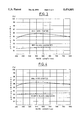
- FIG. 1 is a graph showing the spectral reflectivity of a film of the invention on BK7 glass compared to uncoated glass;
- FIG. 2 is a graph showing the spectral reflectivity of a film of the invention on quartz glass compared to quartz glass which has not been treated;
- FIG. 3 is a graph showing the spectral transmission capacity of a film of the invention on BK7 glass compared to uncoated glass.
- FIG. 4 is a graph showing the spectral transmission capacity of a film of the invention on quartz glass compared to quartz glass which has not been treated.
- the electron beam vaporization at a vaporization rate of 0.2 nm/s up to a film thickness of 108 nm is carried out at a residual gas pressure of 1.3 to 1.5 ⁇ 10 -5 mbar and at an oxygen pressure of 2.7 ⁇ 10 -4 mbar.
- the plates and wedges are removed after a cool-down time of 5 minutes and a delay interval of 50 to 100 minutes. Thereafter, the plates and wedges are tempered in air in an oven at 250° C. for approximately 750 minutes.
- the partial pressure in the vacuum is less than 3 ⁇ 10 -4 mbar. Also, the maximum temperature during tempering is so controlled that it does not exceed 300° C.
- FIGS. 1 and 2 show the trace of the spectral reflectivity for the wedges of glass or quartz glass so treated. These figures also show the trace of the spectral reflectivity compared to the regions of the same wedges to which no film has been applied because of a covering. The reduction of reflection produced by the gallium oxide film is significant in the entire spectral range.
- FIGS. 3 and 4 show the corresponding increase of the transmission of the plates where they have been coated with gallium oxide compared to uncoated regions of these plates.
- the plates are made of glass or quartz glass.
- This value is significantly less than the refractive index n glass of the substrate material and, above all, much less than the refractive index given for gallium oxide as a piece which is greater than 1.8.
- Such a difference of the refractive index of thin film with respect to solid pieces does not occur for other conventional materials for thin optical films (for example MgF 2 ).
- the thin films made of oxidized gallium can be applied to substrates and layers conventional in optics and can be covered with the conventional thin films made also of other materials.
- the gallium oxide film is relatively loose and is therefore not completely smudge proof. For this reason, the gallium oxide film is especially suited for coating the inner-lying surfaces of, for example, lenses in complex optical systems such as photographic objectives, microscope optics, et cetera.
Landscapes
- Chemical & Material Sciences (AREA)
- Physics & Mathematics (AREA)
- General Physics & Mathematics (AREA)
- Chemical Kinetics & Catalysis (AREA)
- Engineering & Computer Science (AREA)
- Materials Engineering (AREA)
- Optics & Photonics (AREA)
- Organic Chemistry (AREA)
- Mechanical Engineering (AREA)
- Metallurgy (AREA)
- Life Sciences & Earth Sciences (AREA)
- General Chemical & Material Sciences (AREA)
- Geochemistry & Mineralogy (AREA)
- Inorganic Chemistry (AREA)
- Surface Treatment Of Glass (AREA)
- Physical Vapour Deposition (AREA)
- Surface Treatment Of Optical Elements (AREA)
Abstract
A thin film of gallium oxidized with oxygen is produced by reactive vapor depositing gallium in a vacuum with oxygen followed by tempering. The refractive index (n) lies in the range of 1.2 to 1.3.
Description
This is a continuation-in-part application of International patent application PCT/EP93/01692, filed Jul. 1, 1993, and claiming priority of German patent application P 42 22 144.7, filed Jul. 6, 1992.
The invention relates to a thin film and a method for producing thin optical films by vapor depositing gallium with oxygen in a vacuum followed by tempering in air.
Thin films are routinely used in optics for coating, silvering, as filters and the like and are produced, inter alia, with commercial apparatus by reactive vapor deposition of metals, inter alia, in a vacuum with oxygen or other reactive partners.
Thin films are especially overcoatings of dielectric substances or metals having the thickness of a few molecular layers up to a thickness in the order of magnitude of wavelengths of visible and infrared light.
Japanese patent publication JP 1,225,315 discloses a method for depositing pure gallium on a substrate. Thin films of gallium nitride and gallium arsenide are known but technical applications of gallium oxide are not known.
The reference text "Handbook of Chemistry and Physics", 71st edition (1990 to 1991), CRC PRESS, Boca Raton USA, page 4-65 lists the refractive index of crystalline Ga2 O3 as n=1.92 to 1.95 and for hydrogenated Ga2 O3. H2 O as n=1.84. The refractive index of other oxides of gallium is not presented.
The article of Hariu et al published in the Japanese Journal of Applied Physics, Volume 16 (1977), pages 841 and 842, discloses a gallium oxide thin film made by reactive vapor deposition. Gallium is thermally evaporated in an 8×10⁻² Torr oxygen atmosphere. Tempering is performed at 1,000° C. The refractive index is only given for the amorphous as-deposited film (not tempered) to be typically 1.6. Accordingly, no suggestion is provided that a thin film of the outstanding antireflective properties (caused by the index of refraction of 1.2) could be obtained.
It is an object of the invention to provide a new material for thin films and especially for antireflection films on glass or quartz glass.
According to a feature of the invention, the film comprises gallium oxidized with oxygen. The film is produced by reactive vapor depositing gallium in the presence of oxygen followed by tempering in air.
It has been surprisingly shown that the refractive index of such a thin film is less than the refractive index of conventional optical glass or quartz glass which is in contrast to the value in the literature for solid gallium oxide. The refractive index (n) of the film of the invention lies in the range of 1.2 to 1.3. From this, the special suitability as an antireflective film for glass or quartz glass is derived.
Electron-beam vaporization is especially advantageous for vapor deposition. Optical elements can carry the thin film of the invention individually or in combination with other thin films.
The invention will now be described with reference to the drawings wherein:
FIG. 1 is a graph showing the spectral reflectivity of a film of the invention on BK7 glass compared to uncoated glass;
FIG. 2 is a graph showing the spectral reflectivity of a film of the invention on quartz glass compared to quartz glass which has not been treated;
FIG. 3 is a graph showing the spectral transmission capacity of a film of the invention on BK7 glass compared to uncoated glass; and,
FIG. 4 is a graph showing the spectral transmission capacity of a film of the invention on quartz glass compared to quartz glass which has not been treated.
Conventional plane-parallel plates and wedges made of optical glass BK7 and of quartz glass SUPRASIL are introduced, after conventional cleaning, into a commercial facility for the reactive vapor deposition of thin films utilizing electron-beam deposition in vacuum. Optical glass BK7 is a product of Schott Glaswerke of Mainz, Germany. The wedges and plates are partially covered in order to later have a comparison between coated and uncoated specimens. Conventional metallic gallium (purity better than 99.9%) is introduced into a copper vaporization crucible.
The electron beam vaporization at a vaporization rate of 0.2 nm/s up to a film thickness of 108 nm is carried out at a residual gas pressure of 1.3 to 1.5×10⁻⁵ mbar and at an oxygen pressure of 2.7×10⁻⁴ mbar. The plates and wedges are removed after a cool-down time of 5 minutes and a delay interval of 50 to 100 minutes. Thereafter, the plates and wedges are tempered in air in an oven at 250° C. for approximately 750 minutes.
According to another feature of the invention, the partial pressure in the vacuum is less than 3×10⁻⁴ mbar. Also, the maximum temperature during tempering is so controlled that it does not exceed 300° C.
FIGS. 1 and 2 show the trace of the spectral reflectivity for the wedges of glass or quartz glass so treated. These figures also show the trace of the spectral reflectivity compared to the regions of the same wedges to which no film has been applied because of a covering. The reduction of reflection produced by the gallium oxide film is significant in the entire spectral range.
FIGS. 3 and 4 show the corresponding increase of the transmission of the plates where they have been coated with gallium oxide compared to uncoated regions of these plates. The plates are made of glass or quartz glass.
The refractive index of the films of the invention on glass as well as on quartz glass was obtained for both at n=1.23 to n=1.25 from the minimum of the reflection reduction; that is, from the reflection R of the λ/4-position in accordance with the known formula ##EQU1## This value is significantly less than the refractive index nglass of the substrate material and, above all, much less than the refractive index given for gallium oxide as a piece which is greater than 1.8.
Such a difference of the refractive index of thin film with respect to solid pieces does not occur for other conventional materials for thin optical films (for example MgF2).
It has been shown that for the production of thin films according to the invention and made from gallium oxidized with oxygen (the gallium need not be present in stoichiometric form as pure Ga2 O3), no special measures of vaporization technology are required. Rather, only the preparation of gallium as a vaporization material and an atmosphere containing oxygen is important.
The thin films made of oxidized gallium can be applied to substrates and layers conventional in optics and can be covered with the conventional thin films made also of other materials.
The structure of the gallium oxide film is relatively loose and is therefore not completely smudge proof. For this reason, the gallium oxide film is especially suited for coating the inner-lying surfaces of, for example, lenses in complex optical systems such as photographic objectives, microscope optics, et cetera.
It is understood that the foregoing description is that of the preferred embodiments of the invention and that various changes and modifications may be made thereto without departing from the spirit and scope of the invention as defined in the appended claims.
Claims (6)
1. A composite comprising a glass or quartz glass substrate upon which is disposed an antireflection film, said film comprising gallium oxidized by oxygen and having an index of refraction in the range of 1.2 to 1.3.
2. A composite comprising an optical element, said optical element being a body of solid transparent material upon which is disposed a thin film, said thin film comprising gallium oxidized by oxygen and having an index of refraction in the range of 1.2 to 1.3.
3. The composite of claim 2, wherein said solid transparent material is glass or quartz glass.
4. The composite of claim 2, wherein said optical element is part of a photographic objective or a microscope.
5. The composite of claim 2, wherein said optical element has an interior surface and said film is applied to said interior surface of said optical element.
6. A composite comprising a solid transparent material substrate upon which is disposed a thin film, said thin film comprising at least a two layer film-stack, wherein the improvement comprises one of the at least two layers being gallium oxidized by oxygen and having an index of refraction in the range of 1.2 to 1.3.
Applications Claiming Priority (2)
| Application Number | Priority Date | Filing Date | Title |
|---|---|---|---|
| DE4222144.7 | 1992-07-06 | ||
| DE4222144 | 1992-07-06 |
Publications (1)
| Publication Number | Publication Date |
|---|---|
| US5474851A true US5474851A (en) | 1995-12-12 |
Family
ID=6462579
Family Applications (1)
| Application Number | Title | Priority Date | Filing Date |
|---|---|---|---|
| US08/206,725 Expired - Fee Related US5474851A (en) | 1992-07-06 | 1994-03-07 | Thin film of gallium oxide and method of producing the film |
Country Status (5)
| Country | Link |
|---|---|
| US (1) | US5474851A (en) |
| JP (1) | JPH07501160A (en) |
| CH (1) | CH685137A5 (en) |
| DE (1) | DE4321301A1 (en) |
| WO (1) | WO1994001792A1 (en) |
Cited By (5)
| Publication number | Priority date | Publication date | Assignee | Title |
|---|---|---|---|---|
| US5597768A (en) * | 1996-03-21 | 1997-01-28 | Motorola, Inc. | Method of forming a Ga2 O3 dielectric layer |
| US6596966B1 (en) * | 1998-12-02 | 2003-07-22 | Lpkf Laser & Electronics Ag | Method for making a marking in a glass body |
| US20050202170A1 (en) * | 2004-03-10 | 2005-09-15 | Remington Michael P.Jr. | Method for depositing gallium oxide coatings on flat glass |
| US20240287675A1 (en) * | 2021-06-18 | 2024-08-29 | L'air Liquide, Societe Anonyme Pour L'etude Et L’Exploitation Des Procedes Georges Claude | Gallium precursors for deposition of gallium-containing oxide films |
| US12258663B2 (en) | 2018-02-14 | 2025-03-25 | Lg Display Co., Ltd. | Apparatus and method of manufacturing oxide film and display apparatus including the oxide film |
Families Citing this family (2)
| Publication number | Priority date | Publication date | Assignee | Title |
|---|---|---|---|---|
| US5550089A (en) * | 1994-03-23 | 1996-08-27 | Lucent Technologies Inc. | Gallium oxide coatings for optoelectronic devices using electron beam evaporation of a high purity single crystal Gd3 Ga5 O12 source. |
| US5451548A (en) * | 1994-03-23 | 1995-09-19 | At&T Corp. | Electron beam deposition of gallium oxide thin films using a single high purity crystal source |
Citations (6)
| Publication number | Priority date | Publication date | Assignee | Title |
|---|---|---|---|---|
| US4187336A (en) * | 1977-04-04 | 1980-02-05 | Gordon Roy G | Non-iridescent glass structures |
| JPS5645092A (en) * | 1979-09-20 | 1981-04-24 | Nippon Telegr & Teleph Corp <Ntt> | Semiconductor luminous element |
| US4331737A (en) * | 1978-04-01 | 1982-05-25 | Zaidan Hojin Handotai Kenkyu Shinkokai | Oxynitride film and its manufacturing method |
| US4371587A (en) * | 1979-12-17 | 1983-02-01 | Hughes Aircraft Company | Low temperature process for depositing oxide layers by photochemical vapor deposition |
| US4595634A (en) * | 1983-08-01 | 1986-06-17 | Gordon Roy G | Coating process for making non-iridescent glass |
| JPH01225315A (en) * | 1988-03-04 | 1989-09-08 | Fuji Electric Co Ltd | Sputtering |
-
1993
- 1993-06-26 DE DE4321301A patent/DE4321301A1/en not_active Withdrawn
- 1993-07-01 CH CH634/94A patent/CH685137A5/en not_active IP Right Cessation
- 1993-07-01 JP JP6502907A patent/JPH07501160A/en active Pending
- 1993-07-01 WO PCT/EP1993/001692 patent/WO1994001792A1/en not_active Ceased
-
1994
- 1994-03-07 US US08/206,725 patent/US5474851A/en not_active Expired - Fee Related
Patent Citations (6)
| Publication number | Priority date | Publication date | Assignee | Title |
|---|---|---|---|---|
| US4187336A (en) * | 1977-04-04 | 1980-02-05 | Gordon Roy G | Non-iridescent glass structures |
| US4331737A (en) * | 1978-04-01 | 1982-05-25 | Zaidan Hojin Handotai Kenkyu Shinkokai | Oxynitride film and its manufacturing method |
| JPS5645092A (en) * | 1979-09-20 | 1981-04-24 | Nippon Telegr & Teleph Corp <Ntt> | Semiconductor luminous element |
| US4371587A (en) * | 1979-12-17 | 1983-02-01 | Hughes Aircraft Company | Low temperature process for depositing oxide layers by photochemical vapor deposition |
| US4595634A (en) * | 1983-08-01 | 1986-06-17 | Gordon Roy G | Coating process for making non-iridescent glass |
| JPH01225315A (en) * | 1988-03-04 | 1989-09-08 | Fuji Electric Co Ltd | Sputtering |
Non-Patent Citations (6)
| Title |
|---|
| "CRC Handbook of Chemistry and Physics", 71st edition (1990 to 1991), CRC Press, Boca Raton USA, pp. 4-65. |
| "Gallium Oxide Thin Film by Reactive Vapour Deposition", by T. Hariu et al., Japanese Journal Applied Physics, vol. 16, (1977, No. 5, pp. 841 to 842). |
| "Optical Properties of Thin Films of Ga2 O3 " by P. Koukal et al. in Scripta Fac. Sci. Not. UJEP Brunensis, Physica 2, vol. 5, (1975), pp. 71 to 82. |
| CRC Handbook of Chemistry and Physics , 71st edition (1990 to 1991), CRC Press, Boca Raton USA, pp. 4 65. * |
| Gallium Oxide Thin Film by Reactive Vapour Deposition , by T. Hariu et al., Japanese Journal Applied Physics, vol. 16, (1977, No. 5, pp. 841 to 842). * |
| Optical Properties of Thin Films of Ga 2 O 3 by P. Koukal et al. in Scripta Fac. Sci. Not. UJEP Brunensis, Physica 2, vol. 5, (1975), pp. 71 to 82. * |
Cited By (9)
| Publication number | Priority date | Publication date | Assignee | Title |
|---|---|---|---|---|
| US5597768A (en) * | 1996-03-21 | 1997-01-28 | Motorola, Inc. | Method of forming a Ga2 O3 dielectric layer |
| US6596966B1 (en) * | 1998-12-02 | 2003-07-22 | Lpkf Laser & Electronics Ag | Method for making a marking in a glass body |
| US20050202170A1 (en) * | 2004-03-10 | 2005-09-15 | Remington Michael P.Jr. | Method for depositing gallium oxide coatings on flat glass |
| WO2005092809A1 (en) * | 2004-03-10 | 2005-10-06 | Pilkington North America, Inc. | Method for depositing gallium oxide coatings on flat glass |
| US7223441B2 (en) * | 2004-03-10 | 2007-05-29 | Pilkington North America, Inc. | Method for depositing gallium oxide coatings on flat glass |
| CN1930099B (en) * | 2004-03-10 | 2011-08-03 | 皮尔金顿北美公司 | Method for depositing gallium oxide coatings on flat glass |
| US12258663B2 (en) | 2018-02-14 | 2025-03-25 | Lg Display Co., Ltd. | Apparatus and method of manufacturing oxide film and display apparatus including the oxide film |
| US20240287675A1 (en) * | 2021-06-18 | 2024-08-29 | L'air Liquide, Societe Anonyme Pour L'etude Et L’Exploitation Des Procedes Georges Claude | Gallium precursors for deposition of gallium-containing oxide films |
| US12467134B2 (en) * | 2021-06-18 | 2025-11-11 | L'Air Liquide, Societe Anonyme pour l'Etude et l'Exploitation des Procedés Georges Claude | Method for deposition of gallium-containing film with gallium precursors |
Also Published As
| Publication number | Publication date |
|---|---|
| WO1994001792A1 (en) | 1994-01-20 |
| JPH07501160A (en) | 1995-02-02 |
| DE4321301A1 (en) | 1994-01-13 |
| CH685137A5 (en) | 1995-03-31 |
Similar Documents
| Publication | Publication Date | Title |
|---|---|---|
| Waldorf et al. | Optical coatings deposited by reactive ion plating | |
| US5958155A (en) | Process for producing thin film | |
| Gilo et al. | Properties of TiO2 films prepared by ion-assisted deposition using a gridless end-Hall ion source | |
| JP2716230B2 (en) | Infrared transparent material | |
| JPH05254887A (en) | Transparent laminated substrate, its use and laminating method, method and device for laminating on base material, and hafnium oxynitride | |
| US5340607A (en) | Vapor-deposition material for the production of high-refraction optical coatings | |
| US4846541A (en) | Interference film filter and an optical waveguide and a method for producing the same | |
| US5474851A (en) | Thin film of gallium oxide and method of producing the film | |
| JP3723580B2 (en) | Vapor deposition materials for the production of medium refractive index optical coatings | |
| US4112142A (en) | Method for the production of light-reflecting layers on a surface of a transparent glass article | |
| JPH07111484B2 (en) | Antireflection film for plastic optical parts and method for forming the same | |
| CN100457680C (en) | Gaseous phase sedimentary material for producing high refractive index optical coating layer and production method of said gaseous phase sedimentary material | |
| JPH07331412A (en) | Optical parts for infrared ray and their production | |
| US20130135712A1 (en) | Yttrium oxide coated optical elements with improved mid-infrared performance | |
| JPH0585778A (en) | Optical parts with antireflection film | |
| JPH0553001A (en) | Multilayered antireflection film of optical parts made of synthetic resin | |
| JP2007156321A (en) | Optical multilayer filter manufacturing method | |
| Bradford et al. | The effect of the substrate temperature on the optical properties of reactively evaporated silicon oxide films | |
| JP3352172B2 (en) | Optical thin film of plastic optical component and method of forming the same | |
| Pulker | Coatings on glass substrates | |
| JPH04260004A (en) | Synthetic resin reflecting mirror | |
| JPH05129277A (en) | Multilayer reflection preventive film | |
| JP2979327B2 (en) | Anti-reflective coating deposited on low melting point substrate | |
| JP3353944B2 (en) | Antireflection film for optical component and optical component formed with this antireflection film | |
| JPH09127304A (en) | Antifungal optical thin film and antireflection film |
Legal Events
| Date | Code | Title | Description |
|---|---|---|---|
| AS | Assignment |
Owner name: CARL-ZEISS-STIFTUNG HEIDENHEIM/BRENZ CARL ZEISS, G Free format text: ASSIGNMENT OF ASSIGNORS INTEREST;ASSIGNOR:GANSWEIN, BERNHARD;REEL/FRAME:006929/0479 Effective date: 19940308 |
|
| FEPP | Fee payment procedure |
Free format text: PAYOR NUMBER ASSIGNED (ORIGINAL EVENT CODE: ASPN); ENTITY STATUS OF PATENT OWNER: LARGE ENTITY |
|
| REMI | Maintenance fee reminder mailed | ||
| LAPS | Lapse for failure to pay maintenance fees | ||
| FP | Lapsed due to failure to pay maintenance fee |
Effective date: 19991212 |
|
| STCH | Information on status: patent discontinuation |
Free format text: PATENT EXPIRED DUE TO NONPAYMENT OF MAINTENANCE FEES UNDER 37 CFR 1.362 |