US5446757A - Code-division-multiple-access-system based on M-ary pulse-position modulated direct-sequence - Google Patents
Code-division-multiple-access-system based on M-ary pulse-position modulated direct-sequence Download PDFInfo
- Publication number
- US5446757A US5446757A US08/077,347 US7734793A US5446757A US 5446757 A US5446757 A US 5446757A US 7734793 A US7734793 A US 7734793A US 5446757 A US5446757 A US 5446757A
- Authority
- US
- United States
- Prior art keywords
- pulse
- sequence
- duty
- bit
- signal
- Prior art date
- Legal status (The legal status is an assumption and is not a legal conclusion. Google has not performed a legal analysis and makes no representation as to the accuracy of the status listed.)
- Expired - Fee Related
Links
Images
Classifications
-
- H—ELECTRICITY
- H04—ELECTRIC COMMUNICATION TECHNIQUE
- H04L—TRANSMISSION OF DIGITAL INFORMATION, e.g. TELEGRAPHIC COMMUNICATION
- H04L25/00—Baseband systems
- H04L25/38—Synchronous or start-stop systems, e.g. for Baudot code
- H04L25/40—Transmitting circuits; Receiving circuits
- H04L25/49—Transmitting circuits; Receiving circuits using code conversion at the transmitter; using predistortion; using insertion of idle bits for obtaining a desired frequency spectrum; using three or more amplitude levels ; Baseband coding techniques specific to data transmission systems
- H04L25/493—Transmitting circuits; Receiving circuits using code conversion at the transmitter; using predistortion; using insertion of idle bits for obtaining a desired frequency spectrum; using three or more amplitude levels ; Baseband coding techniques specific to data transmission systems by transition coding, i.e. the time-position or direction of a transition being encoded before transmission
-
- H—ELECTRICITY
- H03—ELECTRONIC CIRCUITRY
- H03K—PULSE TECHNIQUE
- H03K7/00—Modulating pulses with a continuously-variable modulating signal
- H03K7/04—Position modulation, i.e. PPM
-
- H—ELECTRICITY
- H04—ELECTRIC COMMUNICATION TECHNIQUE
- H04B—TRANSMISSION
- H04B1/00—Details of transmission systems, not covered by a single one of groups H04B3/00 - H04B13/00; Details of transmission systems not characterised by the medium used for transmission
- H04B1/69—Spread spectrum techniques
- H04B1/707—Spread spectrum techniques using direct sequence modulation
-
- H—ELECTRICITY
- H04—ELECTRIC COMMUNICATION TECHNIQUE
- H04B—TRANSMISSION
- H04B14/00—Transmission systems not characterised by the medium used for transmission
- H04B14/02—Transmission systems not characterised by the medium used for transmission characterised by the use of pulse modulation
- H04B14/026—Transmission systems not characterised by the medium used for transmission characterised by the use of pulse modulation using pulse time characteristics modulation, e.g. width, position, interval
-
- H—ELECTRICITY
- H04—ELECTRIC COMMUNICATION TECHNIQUE
- H04J—MULTIPLEX COMMUNICATION
- H04J13/00—Code division multiplex systems
-
- H—ELECTRICITY
- H04—ELECTRIC COMMUNICATION TECHNIQUE
- H04L—TRANSMISSION OF DIGITAL INFORMATION, e.g. TELEGRAPHIC COMMUNICATION
- H04L25/00—Baseband systems
- H04L25/38—Synchronous or start-stop systems, e.g. for Baudot code
- H04L25/40—Transmitting circuits; Receiving circuits
- H04L25/49—Transmitting circuits; Receiving circuits using code conversion at the transmitter; using predistortion; using insertion of idle bits for obtaining a desired frequency spectrum; using three or more amplitude levels ; Baseband coding techniques specific to data transmission systems
- H04L25/4902—Pulse width modulation; Pulse position modulation
-
- H—ELECTRICITY
- H04—ELECTRIC COMMUNICATION TECHNIQUE
- H04J—MULTIPLEX COMMUNICATION
- H04J13/00—Code division multiplex systems
- H04J13/0003—Code application, i.e. aspects relating to how codes are applied to form multiplexed channels
Definitions
- the present invention relates in general to a method of data transmission and reception, and more specifically, to a method of data transmission and reception using code-division-multiple-access (CDMA) technique.
- CDMA code-division-multiple-access
- the spread-spectrum technique is a technique developed since about the mid-1950's. A detailed description of the conventional spread-spectrum systems can be found in a tutorial entitled "Theory of Spread Spectrum Communications--A tutorial” authored by Raymond L. Pickholtz et al. and published on IEEE Trans. Commun., Vol. COM-30, pp. 855-884, May 1982.
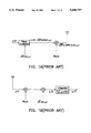
- FIG. 1A-1B The conventional BPSK (Binary-Phase-Shift-Keying) direct sequence spread spectrum communication system is shown in FIG. 1A-1B.
- a multiple access communication system that employs spread spectrum technique is technically termed as a code division multiple access (CDMA) system.
- CDMA code division multiple access
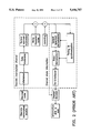
- FIG. 2 The configuration of a basic CDMA system is shown in FIG. 2.
- FIG. 2 A more detail description of the conventional BPSK-DS-SS (or BPSK-DS-CDMA) system of FIG. 1 will be given in the paragraphs under the header "Performance Evaluations.”
- the CDMA technique was developed mainly for capacity reasons. Ever since the analog cellular system started to face its capacity limitation in 1987, research efforts have been conducted on improving the capacity of digital cellular systems. In digital systems, there are three basic multiple access schemes: frequency division multiple access (FDMA), time division multiple access (TDMA), and code division multiple access (CDMA). In theory, it does not matter whether the channel is divided into frequency bands, time slots, or codes; the capacities provided from these three multiple access schemes are the same. However, in cellular systems, we might find that one scheme may be better than the other.
- FDMA frequency division multiple access
- TDMA time division multiple access
- CDMA code division multiple access
- the reason for the improvement in the multiple access capacity of the CDMA system mentioned above is that the capacity of the CDMA system is inversely proportional to cross-correlation noise, which is influenced or can be reduced by: (1) voice activity with a duty factor of approximately 3/8; and (2) spatial isolation through use of multi-beamed or multi-sectored antennas. Therefore if we can find another factor which can reduce the cross-correlation noise, the multiple access capacity will increase correspondingly.
- a primary object of the present invention is to provide a CDMA system by which the multiple access capacity is increased and the transmitting energy is decreased compared to the conventional BPSK-DS-CDMA system.
- a code division multiple access (CDMA) system based on M-ary pulse position modulated direct sequence is provided.
- This system is called a BPSK-MPP-DS-CDMA (Binary-Phase-Shift-Keyed M-ary Pulse-Position-Modulated-Direct-Sequence) system.
- the data source in this system sends out a sequence of data bits with bit duration T.
- the system first converts the serial binary data stream into M parallel bit sequences. These M parallel bit sequences can thus be considered as a sequence of M-bit vectors with each bit having a duration of MT.
- Each M-bit vector is converted into a corresonding block of N cp duty pulses in every interval MT, with each duty pulse set in accordance with a predetermined mapping table to appear in one of the 2 M-1 pulse positions and with a certain polarity.
- This duty pulse train is then modulated with a sample PN p i (t) of the pseudorandom process PN p (t).
- the modulated signal is modulated further by a carrier signal and then is transmitted over the channel of the communication system.
- the received signal is demodulated synchronously by the carrier signal and the pseudorandom sequence signal PN p i (t) to recover each duty pulse block during a duration MT.
- the pulse position and the polarity of the N cp pulses in each received duty pulse block are determined and are used to find the bit pattern represented by each received duty pulse block by using the predetermined mapping table in a reverse manner. In this way, a vector of M parallel data bits are recovered during this duration MT.
- the BPSK-MPP-DS-CDMA system Under the condition that the energy used for one decision (this energy will be defined in the paragraphs under the header "Performance Evaluations") in all concerned systems is equal, the BPSK-MPP-DS-CDMA system according to the present invention has three improved characteristics over the conventional BPSK-DS-CDMA system. These improved characteristics include reduction of cross-correlation noise, an increase in multiple access capacity, and reduction of transmitting energy.
- the multiple access capacity is limited by N cp , that is after the number of users attain N cp , the extra reduction in cross-correlation noise can reduce the bit error rate of the system.
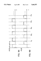
- FIG. 1A shows the block diagram of a transmitter for the conventional BPSK direct sequence spread spectrum system
- FIG. 1B shows the block diagram of a receiver for the conventional BPSK direct sequence spread spectrum system
- FIG. 2 shows a basic CDMA communication system model
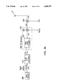
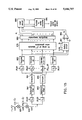
- FIG. 3A shows the block diagram of a BPSK-BPP-DS-CDMA transmitter devised in accordance with the present invention
- FIG. 3B shows the block diagram of a BPSK-BPP-DS-CDMA receiver devised in accordance with the present invention
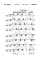
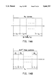
- FIGS. 4A-4D are four waveform patterns, showing the encrypted duty pulse trains generated respectively in response to the bit patterns of four different 2-bit vectors;
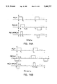
- FIG. 5A shows the waveform of an example of a train of encrypted duty pulses
- FIG. 5B shows an example of a pseudorandom sequence signal used to modulate the pulse train of FIG. 5A
- FIGS. 6A-6B show the waveforms of two control pulse trains used respectively to control the ON/OFF mode of a pair of switches in the receiver of FIG. 3B;
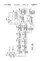
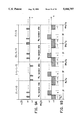
- FIG. 7A shows the block diagram of a BPSK-TPP-DS-CDMA transmitter devised in accordance with the present invention
- FIG. 7B shows the block diagram of a BPSK-TPP-DS-CDMA receiver devised in accordance with the present invention
- FIGS. 8A-8H are eight waveform diagrams, showing the encrypted duty pulse trains generated respectively in response to the bit patterns of eight different 3-bit vectors;
- FIG. 9A shows the waveform of an example of a train of encrypted duty pulses
- FIG. 9B shows an example of a pseudorandom sequence signal used to modulate the pulse train of FIG. 9A;
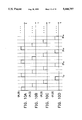
- FIGS. 10A-10D show the timing diagrams of four control pulse trains used respectively to control the ON/OFF mode of an array of four switches in the receiver of FIG. 7B;
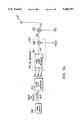
- FIG. 11 shows the block diagram of a modified BPSK-TPP-DS-CDMA receiver devised in accordance with the present invention
- FIGS. 12A-12F show the waveforms of six control pulse trains used respectively to control the ON/OFF mode of the switches S 11 , S 12 , S 21 , S 22 , S 23 , and S 24 in the receiver of FIG. 11;
- FIG. 13A shows the block diagram of a generalized BPSK-MPP-DS-CDMA transmitter devised in accordance with the present invention
- FIG. 13B shows the block diagram of a generalized BPSK-MPP-DS-CDMA receiver devised in accordance with the present invention.
- FIGS. 14A-14B are diagrams used to depict how pulse positions are formed in a generalized M-ary system
- FIG. 15 shows the block diagram of a modified BPSK-MPP-DS-CDMA receiver devised in accordance with the present invention
- the present invention relates to a spread spectrum transmission and reception system based on an M-ary pulse position modulated direct sequence.
- M M-ary pulse position modulated direct sequence.
- BPSK-MPP-DS-CDMA system is described.
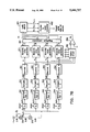
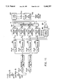
- FIGS. 3A-3B there show a BPSK-BPP-DS-CDMA (binary-phase shift-keyed binary-pulse-position modulated direct-sequence code-division-multiple-access) system devised in accordance with the present invention.
- the transmitter portion of the system is shown in FIG. 3A and the receiver portion of the system is shown in FIG. 3B.
- the transmitter portion of the system which is used to transmit binary signals from a data source 200 to a communication channel, includes a serial-to-parallel converter 210, a BPP-DS modulator 220, and a carrier modulator 230.
- the BPP-DS modulator 220 consists of a duty pulse encryptor 221 and a pulse modulator 222.
- a data bit "1" is transformed into a positive square pulse with a duration of T and a data bit "-1" is transformed into a negative square pulse also with a duration of T at the output of the data source 200.
- Each thus formed 2-bit vector has a bit pattern which may be one of the four possible bit patterns as listed in the following Table-A1:
- each 2-bit vector is processed firstly by the duty-pulse-encryptor 221 and then modulated in the pulse modulator 222 with a pseudorandom sequence signal PN p i (t).
- a number N cp the period of the pseudorandom sequence signal PN p i (t) is used to divide the bit duration 2T into N cp equal intervals with each interval thus having a duration of 2T/N cp .
- the duration 2T/N cp is called the chip T cp of the pseudorandom sequence signal PN p i (t).
- Each chip T cp is divided into two pulse positions (in general the number of pulse positions divided is equal to 2 M-1 for M-ary system).
- the two pulse positions within each T cp are defined as "PP 1 " and "PP 2 ", respectively.
- the duty pulse encryptor 221 includes a built-in one-to-one mapping table defining the generating of a duty pulse train in response to the bit pattern of a 2-bit vector (b 2l b 2l+1 ).
- the preferred embodiment of the present invention incorporates a mapping table having the following mapping relationships:
- the duty pulse encryptor 221 sends out a package of N cp consecutive positive square pulses during the interval 2T with each square pulse appearing at the pulse position defined as "PP 2 ";
- the duty pulse encryptor 221 sends out a package of N cp consecutive negative square pulses during the period 2T with each square pulse appearing at the pulse position defined as "PP 1 .”
- the square pulse in each chip T cp is termed as a "duty pulse.” Only one duty pulse will be present in each chip T cp .
- the duty pulse encryptor 221 will send out a corresponding signal x 1 (t) as illustrated in FIG. 5A.
- the thus formed signal x 1 (t) is subsequently modulated by the pseudorandom sequence signal PN p i (t).
- the timing relationship between x 1 (t) and PN p i (t) can be seen from FIGS. 5A-5B.
- the pseudorandom sequence signal PN p i (t) contains N cp consecutive pseudorandom bits with each bit having a duration of T cp .
- the signal x 2 (t) at the output of pulse modulator 222 is
- the transmitted signal is picked up by the receiver portion of the system located at the receiving end of the channel.
- the demodulated signal y 2 (t) is then multiplied by a local pseudorandom sequence signal PN p i (t- ⁇ i ), which should be in synchronization with the received PN p i (t- ⁇ i ).
- the waveform of the signal y 3 (t) would be identical to x 1 (t) in FIG. 3A if no noise interference were present in the channel. However, no noise interference is only an ideal condition and in practice the signal y 3 (t) may be expressed as:
- I(t) is the cross-correlation noise
- n(t) is the white noise
- a pair of switches S 1 and S 2 with ON/OFF mode thereof being controlled respectively by a first pulse train CP 1 (t) and a second pulse train CP 2 (t), are connected in parallel to the output of the pulse-demodulator 232.
- the waveforms of the two pulse trains CP 1 (t) and CP 2 (t) are shown in FIGS. 6A-6B.
- a pair of matched filters 241 and 242 (which are integrate-and-dump circuits for the present invention) are connected respectively to the switches S 1 and S 2 so that the signals passing through the switches S 1 and S 2 , denoted by y s1 (t) and y s2 (t), are processed by the matched filters 241, 242 and sampled by a pair of samplers 251, 252.
- is the absolute value of ⁇ l ,l 1,2. Further define two decision bits d 1 and d 2 , where d 1 is used to indicate the pulse position of each received duty pulse during each T cp , and d 2 is used to indicate the polarities of duty pulse train.
- the decision bit d 1 can be determined by the following two criteria:
- comparator 291 which compares the magnitude of the signal ⁇ with a zero reference voltage. Accordingly,
- the comparator 291 if ⁇ 0, the comparator 291 generates a logic high voltage representing a bit "1";
- the comparator 291 if ⁇ 0, the comparator 291 generates a logic low voltage representing a bit "-1".
- the subsequent step is to determine the decision bit d 2 , i.e., the polarity of the duty pulse train within 2T.
- This can be implemented by the arrangement of a second comparator 292 connected via two switches S 3 and S 4 respectively to the output of the two summers 261, 262.
- the second comparator 292 compares the input signal with a zero reference voltage. If the magnitude of the input signal is positive, an output bit "1" is generated; and if the magnitude of the input signal is negative, an output bit "-1" is generated. The output bit of the second comparator 292 is taken as the decision bit d 2 .
- a logic circuit 295 is devised to implement the logic relationships of Table-A4, taking (d 1 ,d 2 ) as the input and (b 2l ,b 2l+1 ) as the output.
- the design of the logic circuit 295 is an obvious practice to those who skilled in the art of logic circuit designs, so that detailed circuit diagram thereof will not be illustrated and described.
- Two data bits are thus obtained in parallel, which can be subsequently converted to serial bit stream by a parallel-to-serial converter 296.
- the receiving end thus can fetch from the output of the parallel-to-serial converter 296 a serial bit stream which represents the information sent by the data source 200.
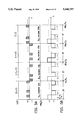
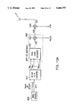
- FIGS. 7A-7B there show a BPSK-TPP-DS-CDMA (TPP stands for "ternary pulse position") digital communication system.
- TPP stands for "ternary pulse position"
- the transmitter portion of the system is shown in FIG. 7A
- the receiver portion of the system is shown in FIG. 7B.
- constituting components that are structurally and functionally the same as those used in the system of FIGS. 3A-3B will not be described in detail again.
- the data bit stream BS is converted by a 3-bit serial-to-parallel converter 310 into three parallel bit streams BS 1 , BS 2 , and and BS 3 ,
- Each thus formed 3-bit vector has a bit pattern which may be one of the eight possible bit patterns as listed in the following Table-B1:
- a number N cp the period of the pseudoramdom sequence signal PN p i (t) shown in FIGS. 7A-7B, is selected to divide the duration 3T into N cp equal intervals.
- Each interval has a duration of 3T/N cp which is referred to as the chip T cp of the pseudorandom sequence signal PN p i (t).
- the four pulse positions are defined respectively as PP 1 ,PP 2 ,PP 3 , and PP 4 .
- a mapping table which defines the generating of a duty pulse train at the output of "Duty Pulse Encryptor 321" in response to the bit pattern of the 3-bit vector at the output of 3-bit S-P converter 310 is predetermined to have the following mapping relationships:
- duty pulse encryptor 321 is triggered to send out a package of N cp consecutive positive square pulses (these square pulses will be hereinafter referred to as "duty pulses") during the bit duration 3T, with each duty pulse appearing at the pulse position defined as PP 1 ;
- the duty pulse encryptor 321 is triggered to send out a package of N cp consecutive positive duty pulses during the bit duration 3T, with each duty pulse appearing at the pulse position defined as PP 2 ;
- the duty pulse encryptor 321 is triggered to send out a package of N cp consecutive positive duty pulses during the bit duration 3T, with each duty pulse appearing at the pulse position defined as PP 4 ;
- the duty pulse encryptor 321 is triggered to send out a package of N cp consecutive negative duty pulses during the bit duration 3T, with each duty pulse appearing at the pulse position defined as PP 4 ;
- the duty pulse encryptor 321 is triggered to send out a package of N cp consecutive negative duty pulses during the bit duration 3T, with each duty pulse appearing at the pulse position defined as PP 3 ;
- the duty pulse encryptor 321 is triggered to send out a package of N cp consecutive negative duty pulses during the bit duration 3T, with each duty pulse appearing at the pulse position defined as PP 2 ;
- the duty pulse encryptor 321 is triggered to send out a package of N cp consecutive negative duty pulses during the bit duration 3T, with each duty pulse appearing at the pulse position defined as PP 1 .
- mapping relationships are summarized in the following Table-B2, or they can be schematically visualized respectively from the diagrams of FIGS. 8A-8H.
- Table-B2 only shows a preferred example of the mapping relationships.
- the duty pulse encryptor 321 will send out a corresponding signal x 1 (t) of duty pulse train as illustrated in FIG. 9A.
- the thus formed duty pulse train x 1 (t) is then modulated in the pulse modulator 322 with a pseudorandom sequence signal PN p i (t) which has period N cp and chip T cp .
- PN p i (t) The timing relationship between x 1 (t) and PN p i (t) can be seen from FIGS. 9A-9B.
- the receiver of the system includes an array of four switches S 1 , S 2 , S 3 , S 4 , which are coupled respectively in subsequence with an array of four matched filters 341, 342, 343, 344, an array of four samplers 351, 352, 353, 354, and an array of four summers 361, 362, 363, 364.
- the ON/OFF modes of the four switches S 1 , S 2 , S 3 , S 4 are respectively controlled by four control pulse sequences CP 1 (t),CP 2 (t),CP 3 (t),CP 4 (t) having waveforms illustrated in FIGS. 10A-10D.
- the appearance of each square pulse in the four control sequences is used to trigger ON the associated switch such that:
- the signals passing the switches S 1 , S 2 , S 3 , or S 4 are processed by the matched filters 341, 342, 343, 344 in accordance with the following integration relationships: ##EQU3## Since there are N cp duty pulses within each bit duration 3T, N cp sampled data of the output of each matched filter are added by using the four summers 361, 362, 363, 364 to obtain four statistics ⁇ 1 , ⁇ 2 , ⁇ 3 , ⁇ 4 , which are given by: ##EQU4## An array of four absolute value generators 371, 372, 373, 374 are used to generate the absolute values of the four statistics ⁇ 1 , ⁇ 2 , ⁇ 3 , ⁇ 4 .
- are compared in a magnitude comparator 381 with one another to find which one has the maximum value. If
- the magnitude comparator 381 has four output bits d 1 , d 2 , d 3 , d 4 (the use of four output bits is just for the convenience of presentation, actually two output bits is sufficient to indicate the results) used to indicate which statistic has the maximum absolute value. The values of these bits are assigned in accordance with the following criteria:
- the outputs of the summers 361, 362, 363, 364 are also connected to a switch circuit 390, which is capable of being controlled by d 1 , d 2 , d 3 , d 4 to allow only one of its four input signals to pass there through.
- the selection is controlled by the four bits d 1 , d 2 , d 3 , d 4 in such a manner that:
- ⁇ 4 is selected as the output.
- ⁇ 1 , ⁇ 2 , ⁇ 3 , and ⁇ 4 that has the maximum absolute value is selected to pass through the switch circuit 390 and thereby compared by a comparator 382 to determine the polarity of the received duty pulse.
- the output of the comparator 382 is a binary signal denoted by d 5 , where
- d 5 -1 if ⁇ l ⁇ 0, i.e., the input signal has a negative magnitude.
- bit pattern represented by the received N cp duty pulses can be determined after the five decision bits (d 1 ,d 2 ,d 3 ,d 4 ,d 5 ) are determined. These are listed in the following Table-B4:
- a logic circuit 401 is built to implement the truth table defined in Table-B4.
- the three parallel output bits of the logic circuit 401 can be converted into serial bit sequence by a parallel-to-serial converter 402 such that the data bit stream originally sent out from the data source is obtained.
- FIG. 11 we show a modified receiver of the BPSK-TPP-DS-CDMA system.
- the ON/OFF modes of the switches S 11 , and S 12 are controlled respectively by the pulse trains CP 11 (t) and CP 12 (t) shown in FIGS. 12A-12B
- the ON/OFF modes of the switches S 21 , S 22 , S 23 , and S 24 are controlled respectively by the pulse trains CP 21 (t), CP 22 (t), CP 23 (t), and CP 24 (t) such that
- modified BPSK-TPP-DS-CDMA receiver shown in FIG. 11 has same function as BPSK-TPP-DS-CDMA receiver shown in FIG. 7B, and thus the detail description of this modified receiver thereof will not be given.
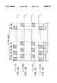
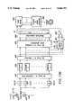
- FIGS. 13A-13B A generalized M-ary system is shown in FIGS. 13A-13B, which is referred to as a BPSK-MPP-DS-CDMA system.
- the transmitter portion of the system is shown in FIG. 13A, and the receiver portion of the system is shown in FIG. 13B.
- the circuit structures for all systems with different selections of M are basically the same. Therefore, for the generalized M-ary system shown in FIGS. 13A-13B, only those components that are particularly related to the selected M will be described.
- an M-bit serial-to-parallel converter 910 is used to convert the input serial data bit stream into M parallel bit streams, or in other words, into a sequence of M-bit vectors with the duration of each M-bit vector equals MT.
- Each T cp is divided into 2 M-1 pulse positions with each pulse position having a duration T s as shown in FIG.
- each pulse position can accommodate either a positive pulse or a negative pulse, they built 2 M possible duty-pulse-train patterns so a one-to-one mapping relationship can be established between the bit pattern of an M-bit vector, which has 2 M possible combinations, and the 2 M possible duty-pulse-train patterns.
- FIG. 15 we show a modified receiver of the BPSK-MPP-DS-CDMA system. Functional operations of each component in the circuit is the same as that used in FIG. 11, so that the detail description of this modified receiver thereof will not be given.
- the BPSK-MPP-DS-CDMA system has three improved characteristics over the conventional BPSK-DS-CDMA system. These improved characteristics include:
- the cross-correlation noise is improved by a factor of M2 M-1 :
- the multiple access capacity is not limitted by the period N cp of the pseudorandom process PN p (t), then under the constraints of same bandwidth and same bit error rate, the multiple access capacity is improved by a factor at least of:
- the extra reduction in cross-correlation noise can reduce the bit error rate of the system.
- the transmitting energy of the BPSK-MPP-DS-CDMA system is only 1/M of the transmitting energy of the conventional BPSK-DS-CDMA system, and thus (M-1)/M of the transmitting energy is saved.
- FIGS. 1A-1B show the conventional BPSK-DS-CDMA system.
- the PN i (t) in FIGS. 1A-1B is a sample of a pseudorandom process PN(t) having chip T c and period N c .
- This PN i (t) is used as the signature of the i-th user and is used in FIG. 1A to modulate the signal x i (t). It also used in FIG. 1B to demodulate the received signal y(t).
- FIGS. 3A-3B show the BPSK-BPP-DS-CDMA system.
- the PN p i (t) in FIGS. 3A-3B is a sample of a pseudorandom process PN p (t) which has period N cp and chip T cp .
- the index p is used to distinguish the process PN p (t) from the pseudorandom process PN(t) used in the conventional BPSK-DS-CDMA system.
- the PN p i (t) is used as the signature of the i-th user.
- the binary data signal d i (t) is multiplexed by the serial -to- parallel converter 210 into two parallel data sequences ##EQU25## where P 2T (t) has a duration 2T.
- P 2T (t) has a duration 2T.
- the bandwidths used in the conventional BPSK-DS-CDMA and BPSK-BPP-DS-CDMA system are assumed to be the same.
- the amount of energy used for one decision in both systems are assumed to be equal to PT.
- the received signal can then be represented as ##EQU29##
- H 2 The signal present in PP 2 .
- N I /2 represents the two sided psd of the total interference noise before the matched filters 241, 242, then ##EQU39## 2.2
- d j is defined as the vector (d -1 j , d 0 j ) and d -1 j , d 0 j are two consecutive data bits of PN c i (t) defined in Eq.(48).
- the functions R ji 1 , R ji 1 , R ji 2 , and R ji 2 can be derived respectively as ##EQU42## where, for convenience, the subscript j of ⁇ j has been omitted.
- the signal-to-noise ratios in the pulse positions PP 1 and PP 2 are defined respectively as
- FIGS. 7A-7B show the BPSK-TPP-DS-CDMA system.
- the PN p i (t) in these figures is also a sample of a pseudorandom process PN p (t) having chip T cp and period N cp .
- This PN p i (t) is also used as the signature of the i-th user.
- the bandwidths and the amount of energy used for one decision in the conventional BPSK-DS-CDMA and BPSK-TPP-DS-CDMA systems are assumed to be the same.
- H 4 The signal present in interval PP 4 .
- the psd S c11 ji (f, ⁇ ) of PN c1 j (t- ⁇ )PN c1 1 (t)cos ⁇ j is nozero for 0 ⁇ T s and 3T s ⁇ T cp but is zero for T s ⁇ 3T s .
- the signal-to-noise ratio in PP 1 , PP 2 , PP 3 , or PP 4 , of the BPSK-TPP-DS-CDMA system can be derived as ##EQU53##
- J-1)PT s /9>>N 0 /2 we have ##EQU54## Compared Eq.(98) to Eq.(25), that is compared to the SNR of the conventional BPSK-DS-CDMA system, the SNR is improved by a factor of 12.
- E b in Eq.(103) is the amount of energy used for one decision in the BPSK-TPP-DS-CDMA system.
- the amplitude of the transmitted signal is ⁇ 8P/3and can present only in PP 1 , PP 2 , PP 3 , or PP 4 , thus two-thirds of the transmitting energy is saved.
- FIGS. 13A-13B show the BPSK-MPP-DS-CDMA system.
- the PN p i (t) in these two figures is a sample of a pseudorandom process PN p (t) having chip T cp and period N cp .
- This PN p i (t) is used as the signature of the i-th user.
- B M (b Ml ,b Ml+1 , . . . ,b Ml+M-1 ) with the duration of the vector B M equal to MT. Since b l ⁇ 1,-1 ⁇ for every l, there are 2I possible vectors within every MT duration.
- each PN cn i (t) to one of the 2I possible B M vectors.
- the transmitted signal x 3 (t) can then be represented as ##EQU60##
- the received signal can be represented as ##EQU61##
Landscapes
- Engineering & Computer Science (AREA)
- Computer Networks & Wireless Communication (AREA)
- Signal Processing (AREA)
- Physics & Mathematics (AREA)
- Spectroscopy & Molecular Physics (AREA)
- Dc Digital Transmission (AREA)
- Digital Transmission Methods That Use Modulated Carrier Waves (AREA)
Abstract
A BPSK-MPP-DS-CDMA system is devised using a pulse position modulated direct sequence technique. Under the same bandwidth, same energy used for one decision, and same bit error rate conditions, if the number of users is less than the period Ncp of the pseudorandom sequence signal PNp i (t) used in the BPSK-MPP-DS-CDMA system, the multiple access capacities of the binary (M=2), ternary (M=3), quaternary (M=4), and pentary (M=5) BPSK-MPP-DS-CDMA systems according to the present invention are respectively at least 2, 5.34, 13.28, and 26.4 times greater than that of the conventional BPSK-DS-CDMA systems. On the other hand, if the number of users attains Ncp, the multiple access capacity can not increase any more, however, the bit error rate of the system will be reduced. Furthermore, (M-1)/M transmitting energy is saved.
Description
1. Field of the Invention
The present invention relates in general to a method of data transmission and reception, and more specifically, to a method of data transmission and reception using code-division-multiple-access (CDMA) technique.
2. Description of Prior Art
The spread-spectrum technique is a technique developed since about the mid-1950's. A detailed description of the conventional spread-spectrum systems can be found in a tutorial entitled "Theory of Spread Spectrum Communications--A Tutorial" authored by Raymond L. Pickholtz et al. and published on IEEE Trans. Commun., Vol. COM-30, pp. 855-884, May 1982.
The conventional BPSK (Binary-Phase-Shift-Keying) direct sequence spread spectrum communication system is shown in FIG. 1A-1B. A multiple access communication system that employs spread spectrum technique is technically termed as a code division multiple access (CDMA) system. The configuration of a basic CDMA system is shown in FIG. 2. A more detail description of the conventional BPSK-DS-SS (or BPSK-DS-CDMA) system of FIG. 1 will be given in the paragraphs under the header "Performance Evaluations."
The CDMA technique was developed mainly for capacity reasons. Ever since the analog cellular system started to face its capacity limitation in 1987, research efforts have been conducted on improving the capacity of digital cellular systems. In digital systems, there are three basic multiple access schemes: frequency division multiple access (FDMA), time division multiple access (TDMA), and code division multiple access (CDMA). In theory, it does not matter whether the channel is divided into frequency bands, time slots, or codes; the capacities provided from these three multiple access schemes are the same. However, in cellular systems, we might find that one scheme may be better than the other.
A list of technical references pertinent to the subject matter of the present invention is given below:
[1] "Overview of Cellular CDMA", by William C. Y. Lee, IEEE Trans. Veh. Tech., Vol. 40, No. 2, pp. 291-302, May 1991.
[2] "On the Capacity of a Cellular CDMA System", by A. J. Viterbi, L. A. Weaver, and C. E. Wheatley III, IEEE Trans. Veh. Tech., Vol. 40, No. 2, pp. 303-312, May 1991.
[3]"A Statistical Analysis of On-off Patterns in 16 Conversations", by P. T. Brady, Bell Syst. Tech. J., Vol. 47, pp. 73-91, Jan. 1968.
[4]"Coherent Spread Spectrum Systems", by J. K. Holmes, John Wiley and Sons, New York, pp. 388-389, 1982.
[5] "Error Probability of Asynchronous Spread Spectrum Multiple Access Communications Systems", by K. Yao, IEEE Trans. Commum. Vol. COM-25, pp. 803-807, 1977.
[6] "Direct-Sequence Spread Spectrum Multiple-Access Communications with Random Signature Sequences: Large Deviations Analysis", by J. S. Sadowsky and R. K. Bahr, IEEE Trans. Inform. Theory Vol. 37, No. 3, pp. 514-527, May 1991.
[7] "Digital Communications and Spread Spectrum Systems", by R. E. Ziemer and R. L. Peterson, Macmillan, New York, Ch. 11, 1985.
[8] "Spread Spectrum Multiple Access Communications, Multi-User communication Systems", by M. B. Pursley, edited by G. Longo, Springer-Verlag, N.Y. pp. 139-199, 1981.
[9] "Performance Evaluation for Phase-Coded Spread-Spectrum Multiple-Access Communication-- Part II: Code Sequence Analysis", by M. B. Pursley and D. V. Sarwate, IEEE Trans. Commun., Vol. Com-25, No. 8, pp. 800-803, August 1977.
Remarkable results have been derived in the pertinent reference [2], "On the Capacity of a Cellular CDMA System" by A. J. Viterbi et al. This technical paper shows that the net improvement in the capacity of CDMA systems is four to six times better than that of a digital TDMA or FDMA system, and nearly 20 times better than that of current analog FM/FDMA system. Therefore, the CDMA scheme may become a major system in future communication systems.
The reason for the improvement in the multiple access capacity of the CDMA system mentioned above is that the capacity of the CDMA system is inversely proportional to cross-correlation noise, which is influenced or can be reduced by: (1) voice activity with a duty factor of approximately 3/8; and (2) spatial isolation through use of multi-beamed or multi-sectored antennas. Therefore if we can find another factor which can reduce the cross-correlation noise, the multiple access capacity will increase correspondingly.
A primary object of the present invention is to provide a CDMA system by which the multiple access capacity is increased and the transmitting energy is decreased compared to the conventional BPSK-DS-CDMA system.
In accordance with the above objects, a code division multiple access (CDMA) system based on M-ary pulse position modulated direct sequence is provided. This system is called a BPSK-MPP-DS-CDMA (Binary-Phase-Shift-Keyed M-ary Pulse-Position-Modulated-Direct-Sequence) system. The data source in this system sends out a sequence of data bits with bit duration T. According to the present invention the system first converts the serial binary data stream into M parallel bit sequences. These M parallel bit sequences can thus be considered as a sequence of M-bit vectors with each bit having a duration of MT. A number Ncp, which is the period of a pseudorandom process PNp (t), is selected to divide each MT duration into Ncp intervals with every interval having a duration Tcp, where Tcp =MT/Ncp. Each interval Tcp is further divided into 2M-1 pulse positions, each pulse position having a duration Ts, Ts =Tcp /2M-1. Each M-bit vector is converted into a corresonding block of Ncp duty pulses in every interval MT, with each duty pulse set in accordance with a predetermined mapping table to appear in one of the 2M-1 pulse positions and with a certain polarity. This duty pulse train is then modulated with a sample PNp i (t) of the pseudorandom process PNp (t). The modulated signal is modulated further by a carrier signal and then is transmitted over the channel of the communication system.
In the receiving end of the communication system, the received signal is demodulated synchronously by the carrier signal and the pseudorandom sequence signal PNp i (t) to recover each duty pulse block during a duration MT. The pulse position and the polarity of the Ncp pulses in each received duty pulse block are determined and are used to find the bit pattern represented by each received duty pulse block by using the predetermined mapping table in a reverse manner. In this way, a vector of M parallel data bits are recovered during this duration MT.
Under the condition that the energy used for one decision (this energy will be defined in the paragraphs under the header "Performance Evaluations") in all concerned systems is equal, the BPSK-MPP-DS-CDMA system according to the present invention has three improved characteristics over the conventional BPSK-DS-CDMA system. These improved characteristics include reduction of cross-correlation noise, an increase in multiple access capacity, and reduction of transmitting energy.
The cross-correlation noise is reduced by a factor of 4 if the system is based on M=2; 12 if the system is based on M=3, 32 if the system is based on M=4, and 80 if the system is based on M=5. If the multiple access capacity is not limited by the period Ncp of the pseudorandom sequence signal PNp i (t), then under the same bandwidth and same bit error rate constraints, the multiple access capacity is improved by a factor at least of 2 if the system is based on M=2; 5.34 if the system is based on M=3; 13.28 if the system is based on M=4; and 26.4 if the system is based on M=5. Conversely, if the multiple access capacity is limited by Ncp, that is after the number of users attain Ncp, the extra reduction in cross-correlation noise can reduce the bit error rate of the system.
For a general M-ary system, the tramsmitting energy is only 1/M of that in the conventional system, i.e., (M-1)/M of the transmitting energy is saved. The proofs of these results will be given in the performance evaluation of the prefered embodiment section.
The present invention can be more fully understood by reading the subsequent detailed description of the preferred embodiments thereof with references made to the accompanying drawings, wherein:
For the Conventional BPSK-DS-SS System:
FIG. 1A shows the block diagram of a transmitter for the conventional BPSK direct sequence spread spectrum system;
FIG. 1B shows the block diagram of a receiver for the conventional BPSK direct sequence spread spectrum system;
FIG. 2 shows a basic CDMA communication system model;
For the BPSK-BPP-DS-CDMA System:
FIG. 3A shows the block diagram of a BPSK-BPP-DS-CDMA transmitter devised in accordance with the present invention;
FIG. 3B shows the block diagram of a BPSK-BPP-DS-CDMA receiver devised in accordance with the present invention;
FIGS. 4A-4D are four waveform patterns, showing the encrypted duty pulse trains generated respectively in response to the bit patterns of four different 2-bit vectors;
FIG. 5A shows the waveform of an example of a train of encrypted duty pulses;
FIG. 5B shows an example of a pseudorandom sequence signal used to modulate the pulse train of FIG. 5A;
FIGS. 6A-6B show the waveforms of two control pulse trains used respectively to control the ON/OFF mode of a pair of switches in the receiver of FIG. 3B;
For the BPSK-TPP-DS-CDMA System:
FIG. 7A shows the block diagram of a BPSK-TPP-DS-CDMA transmitter devised in accordance with the present invention;
FIG. 7B shows the block diagram of a BPSK-TPP-DS-CDMA receiver devised in accordance with the present invention;
FIGS. 8A-8H are eight waveform diagrams, showing the encrypted duty pulse trains generated respectively in response to the bit patterns of eight different 3-bit vectors;
FIG. 9A shows the waveform of an example of a train of encrypted duty pulses;
FIG. 9B shows an example of a pseudorandom sequence signal used to modulate the pulse train of FIG. 9A;
FIGS. 10A-10D show the timing diagrams of four control pulse trains used respectively to control the ON/OFF mode of an array of four switches in the receiver of FIG. 7B;
FIG. 11 shows the block diagram of a modified BPSK-TPP-DS-CDMA receiver devised in accordance with the present invention;
FIGS. 12A-12F show the waveforms of six control pulse trains used respectively to control the ON/OFF mode of the switches S11, S12, S21, S22, S23, and S24 in the receiver of FIG. 11;
For the BPSK-MPP-DS-CDMA System:
FIG. 13A shows the block diagram of a generalized BPSK-MPP-DS-CDMA transmitter devised in accordance with the present invention;
FIG. 13B shows the block diagram of a generalized BPSK-MPP-DS-CDMA receiver devised in accordance with the present invention; and
FIGS. 14A-14B are diagrams used to depict how pulse positions are formed in a generalized M-ary system;
FIG. 15 shows the block diagram of a modified BPSK-MPP-DS-CDMA receiver devised in accordance with the present invention;
For Performance Evaluations:
FIGS. 16A-16B show a set of typical cross-correlated waveforms of PNc1 j (t-ε)PNc1 i (t) for M=3.
The present invention relates to a spread spectrum transmission and reception system based on an M-ary pulse position modulated direct sequence. In the following detailed descriptions, examples will be given for the cases of M=2 and M=3. Finally, a generalized BPSK-MPP-DS-CDMA system is described.
Referring to FIGS. 3A-3B, there show a BPSK-BPP-DS-CDMA (binary-phase shift-keyed binary-pulse-position modulated direct-sequence code-division-multiple-access) system devised in accordance with the present invention. The transmitter portion of the system is shown in FIG. 3A and the receiver portion of the system is shown in FIG. 3B.
The transmitter portion of the system, which is used to transmit binary signals from a data source 200 to a communication channel, includes a serial-to-parallel converter 210, a BPP-DS modulator 220, and a carrier modulator 230. The BPP-DS modulator 220 consists of a duty pulse encryptor 221 and a pulse modulator 222.
In practice, a data bit "1" is transformed into a positive square pulse with a duration of T and a data bit "-1" is transformed into a negative square pulse also with a duration of T at the output of the data source 200. When a data bit stream BS=(b0, b1, b2, . . . , bn-1. . . ) is sent out from the data source 200 with a bit duration of T and is to be transmitted over the communication channel, the data bit stream BS is first converted by the serial-to-parallel converter 210 into two parallel bit streams BS1 and BS2, BS1 =(b0, b2, b4, . . . , b2l, . . . ) and BS2 =(b1, b3, b5, . . . b2l+1, . . . ). However, the duration of each bit in BS1 and BS2 is 2T. Consequently, the 2-bit serial-to-parallel converter 210 sends out a sequence of 2-bit vectors (b2l, b2l+1), l =0,1,2,, . . . , to the BPP-DS modulator 220. Each thus formed 2-bit vector has a bit pattern which may be one of the four possible bit patterns as listed in the following Table-A1:
              TABLE A1
______________________________________
(b.sub.2l, b.sub.2l+1)
______________________________________
(1, 1)
(1, -1)
(-1, 1)
(-1, -1)
______________________________________
In the BPP-DS modulator 220, each 2-bit vector is processed firstly by the duty-pulse-encryptor 221 and then modulated in the pulse modulator 222 with a pseudorandom sequence signal PNp i (t). In the present invention, a number Ncp, the period of the pseudorandom sequence signal PNp i (t), is used to divide the bit duration 2T into Ncp equal intervals with each interval thus having a duration of 2T/Ncp. The duration 2T/Ncp is called the chip Tcp of the pseudorandom sequence signal PNp i (t). Each chip Tcp is divided into two pulse positions (in general the number of pulse positions divided is equal to 2M-1 for M-ary system). The duration of each pulse position is Ts, Ts =Tcp /2. The two pulse positions within each Tcp are defined as "PP1 " and "PP2 ", respectively.
The duty pulse encryptor 221 includes a built-in one-to-one mapping table defining the generating of a duty pulse train in response to the bit pattern of a 2-bit vector (b2l b2l+1). The preferred embodiment of the present invention incorporates a mapping table having the following mapping relationships:
(a) if the input 2-bit vector is (1, 1), the duty pulse encryptor 221 sends out a package of Ncp consecutive positive square pulses during the interval 2T with each square pulse appearing at the pulse position defined as "PP1 ";
(b) if the input 2-bit vector is (1,-1), the duty pulse encryptor 221 sends out a package of Ncp consecutive positive square pulses during the interval 2T with each square pulse appearing at the pulse position defined as "PP2 ";
(c) if the input 2-bit vector is (-1, 1), the duty pulse encryptor 221 sends out a package of Ncp consecutive negative square pulses during the interval 2T with each square pulse appearing at the pulse position defined as "PP2 "; and
(d) if the input 2-bit vector is (-1,-1), the duty pulse encryptor 221 sends out a package of Ncp consecutive negative square pulses during the period 2T with each square pulse appearing at the pulse position defined as "PP1."
The foregoing mapping relationships are summarized in the following Table-A2. They can also be schematically visualized respectively from the diagrams of FIGS. 4A-4D.
              TABLE A2
______________________________________
Bit Pattern    encrypted Duty Pulse
(b.sub.2l, b.sub.2l+1)
               Pulse Position
                          Polarity
______________________________________
(1, 1)         PP.sub.1   +1
(1, -1)        PP.sub.2   +1
(-1, 1)        PP.sub.2   -1
(-1, -1)       PP.sub.1   -1
______________________________________
The square pulse in each chip Tcp is termed as a "duty pulse." Only one duty pulse will be present in each chip Tcp. For example, if the leading eight bits in the bit stream BS are (1, -1, -1, -1, -1, 1, 1, 1), then the duty pulse encryptor 221 will send out a corresponding signal x1 (t) as illustrated in FIG. 5A. The thus formed signal x1 (t) is subsequently modulated by the pseudorandom sequence signal PNp i (t). The timing relationship between x1 (t) and PNp i (t) can be seen from FIGS. 5A-5B. The pseudorandom sequence signal PNp i (t) contains Ncp consecutive pseudorandom bits with each bit having a duration of Tcp. The signal x2 (t) at the output of pulse modulator 222 is
x.sub.2 (t)=x.sub.1 (t)PN.sub.p.sup.i (t), (1)
which is subsequently modulated at the carrier modulator 230 by a sinusoidal signal C(t)=√2P sin(ω0 t) to obtain a modulated signal x3 (t) and thereby transmitted through the communication channel to its destination.
Referring back to FIG. 3B, the transmitted signal is picked up by the receiver portion of the system located at the receiving end of the channel. For noise free situation, the received signal is y1 (t)=Ax3 (t-τi), where "A" is the amplitude of y1 (t), and τi is the transmission delay of x3 (t). The signal y1 (t) is demodulated by multiplying it with a sinusoidal signal C(t-τi)=√2 sin ω0 (t-τi), where τi is the estimate of τi. Since the purpose of this description is only to demonstrate the operation of the system, A=1 and τi =τi =0 can be assumed without the loss of generality. The demodulated signal y2 (t) is then multiplied by a local pseudorandom sequence signal PNp i (t-τi), which should be in synchronization with the received PNp i (t-τi). The waveform of the signal y3 (t) would be identical to x1 (t) in FIG. 3A if no noise interference were present in the channel. However, no noise interference is only an ideal condition and in practice the signal y3 (t) may be expressed as:
y.sub.3 (t)=x.sub.1 (t)+I(t)+n(t), (2)
where I(t) is the cross-correlation noise, and n(t) is the white noise.
A pair of switches S1 and S2, with ON/OFF mode thereof being controlled respectively by a first pulse train CP1 (t) and a second pulse train CP2 (t), are connected in parallel to the output of the pulse-demodulator 232. The waveforms of the two pulse trains CP1 (t) and CP2 (t) are shown in FIGS. 6A-6B. Each of the two pulse trains CP1 (t) and CP2 (t) is a periodic pulse train having pulse duration Ts and period exactly equal to Tcp, where Ts =Tcp /2. The appearance of one square pulse in the pulse train CP1 (t) will actuate the switch S1 to be turned ON; and the appearing of one square pulse in the pulse train CP2 (t) will actuate the switch S2 to be turned ON. A pair of matched filters 241 and 242 (which are integrate-and-dump circuits for the present invention) are connected respectively to the switches S1 and S2 so that the signals passing through the switches S1 and S2, denoted by ys1 (t) and ys2 (t), are processed by the matched filters 241, 242 and sampled by a pair of samplers 251, 252. The outputs of the samplers 251, and 252 are denoted by z1 (k) and z2 (k), which are respectively given by: ##EQU1## where k=1,2, . . . , Ncp
A pair of summers 261, 262 are used respectively to sum up the two outputs z1 (k), z2 (k) for k=1,2, . . . , Ncp. The output signals of the two summers 261, 262 are referred to as "statistics" and are denoted by Λl, l=1, 2, which are respectively given by: ##EQU2## Define a statistic Λ=|Λ1 |-|Λ2 |, where |Λl | is the absolute value of Λl,l=1,2. Further define two decision bits d1 and d2, where d1 is used to indicate the pulse position of each received duty pulse during each Tcp, and d2 is used to indicate the polarities of duty pulse train.
The following Table-A3 can be used to determined the values of d1 and d2 in accordance with received duty pulse:
              TABLE A3
______________________________________
Received Duty Pulse Decision Bits
Pulse Position Polarity (d.sub.1, d.sub.2)
______________________________________
PP.sub.1       +1       (1, 1)
PP.sub.2       +1       (-1, 1)
PP.sub.2       -1       (-1, -1)
PP.sub.1       -1       (1, -1)
______________________________________
The decision bit d1 can be determined by the following two criteria:
(1) if Λ≧0, then d1 =1, and
(2) if Λ<0, then d1 =-1.
These two criteria can be implemented by a comparator 291, which compares the magnitude of the signal Λ with a zero reference voltage. Accordingly,
if Λ≧0, the comparator 291 generates a logic high voltage representing a bit "1"; and
if Λ<0, the comparator 291 generates a logic low voltage representing a bit "-1".
The subsequent step is to determine the decision bit d2, i.e., the polarity of the duty pulse train within 2T. This can be implemented by the arrangement of a second comparator 292 connected via two switches S3 and S4 respectively to the output of the two summers 261, 262. The decision bit d1, which has been already determined at this time, is used to control the ON/OFF of the two switches S3, S4 in such a way that if d1 =1, the switch S3 is triggered ON and the switch S4 is triggered OFF, thereby causing only the signal Λ1 to be passed to the second comparator 292; and if d1 =-1, the switch S3 is triggered OFF and the switch S4 is triggered ON, thereby causing only the signal Λ2 to be passed to the second comparator 292.
The second comparator 292 compares the input signal with a zero reference voltage. If the magnitude of the input signal is positive, an output bit "1" is generated; and if the magnitude of the input signal is negative, an output bit "-1" is generated. The output bit of the second comparator 292 is taken as the decision bit d2.
Based on the two decision bits (d1,d2), the bit pattern represented by the received Ncp duty pulses, denoted here in the receiver portion as (b2l, bl+1), can be determined. In accordance with the foregoing two predefined Table-A2 and Table-A3, a table listing logic relationships between (b2l, b2l+1) and (d1, d2) can be obtained as Table-A4 shown below:
              TABLE A4
______________________________________
Decision Bits
             Deciphered Bit Pattern
______________________________________
(d.sub.1, d.sub.2)
             (b.sub.2l, b.sub.2l+1)
(1, 1)       (1, 1)
(-1, 1)      (1, -1)
(-1, -1)     (-1, 1)
(1, -1)      (-1, -1)
______________________________________
A logic circuit 295 is devised to implement the logic relationships of Table-A4, taking (d1,d2) as the input and (b2l,b2l+1) as the output. The design of the logic circuit 295 is an obvious practice to those who skilled in the art of logic circuit designs, so that detailed circuit diagram thereof will not be illustrated and described.
Two data bits are thus obtained in parallel, which can be subsequently converted to serial bit stream by a parallel-to-serial converter 296. The receiving end thus can fetch from the output of the parallel-to-serial converter 296 a serial bit stream which represents the information sent by the data source 200.
Referring to FIGS. 7A-7B, there show a BPSK-TPP-DS-CDMA (TPP stands for "ternary pulse position") digital communication system. The transmitter portion of the system is shown in FIG. 7A, and the receiver portion of the system is shown in FIG. 7B. In the subsequent descriptions for the system of FIGS. 7A-7B, constituting components that are structurally and functionally the same as those used in the system of FIGS. 3A-3B will not be described in detail again.
In FIG. 7A, the data bit stream BS is converted by a 3-bit serial-to-parallel converter 310 into three parallel bit streams BS1, BS2, and and BS3,
BS.sub.1 =(b.sub.0, b.sub.3, b.sub.6, . . . , b.sub.3l, . . . ) (7)
BS.sub.2 =(b.sub.1, b.sub.4, b.sub.7, . . . , b.sub.3l+1, . . . ) (8)
BS.sub.3 =(b.sub.2, b.sub.5, b.sub.8, . . . , b.sub.3l+2, . . . ) (9)
However, the duration of each bit in BS1, BS2, and BS3 is now changed to 3T. Consequently, the 3-bit serial-to-parallel converter 310 sends out a sequence of 3-bit vectors (b3l, b3l+1, b3l+2),l=0,1,2,, . . . , to the TPP-DS modulator 320. Each thus formed 3-bit vector has a bit pattern which may be one of the eight possible bit patterns as listed in the following Table-B1:
              TABLE B1
______________________________________
(b.sub.3l, b.sub.3l+1, b.sub.3l+2)
______________________________________
(1, 1, 1)
(1, 1, -1)
(1, -1, 1)
(1, -1, -1)
(-1, 1, 1)
(-1, 1, -1)
(-1, -1, 1)
(-1, -1, -1)
______________________________________
Referring to FIGS. 8A-8H, a number Ncp, the period of the pseudoramdom sequence signal PNp i (t) shown in FIGS. 7A-7B, is selected to divide the duration 3T into Ncp equal intervals. Each interval has a duration of 3T/Ncp which is referred to as the chip Tcp of the pseudorandom sequence signal PNp i (t). Each Tcp is divided further by four (in general this number is equal to 2M-1) into four pulse positions with each pulse position having a duration of Ts, where Ts =Tcp /4. The four pulse positions are defined respectively as PP1,PP2,PP3, and PP4.
A mapping table, which defines the generating of a duty pulse train at the output of "Duty Pulse Encryptor 321" in response to the bit pattern of the 3-bit vector at the output of 3-bit S-P converter 310 is predetermined to have the following mapping relationships:
(a) if the 3-bit vector is (1, 1, 1), the duty pulse encryptor 321 is triggered to send out a package of Ncp consecutive positive square pulses (these square pulses will be hereinafter referred to as "duty pulses") during the bit duration 3T, with each duty pulse appearing at the pulse position defined as PP1 ;
(b) if the 3-bit vector is (1, 1, -1), the duty pulse encryptor 321 is triggered to send out a package of Ncp consecutive positive duty pulses during the bit duration 3T, with each duty pulse appearing at the pulse position defined as PP2 ;
(c) if the 3-bit vector is (1, -1, 1), the duty pulse encryptor 321 is triggered to send out a package of Ncp consecutive positive duty pulses during the bit duration 3T, with each duty pulse appearing at the pulse position defined as PP3 ;
(d) if the 3-bit vector is (1, -1, -1), the duty pulse encryptor 321 is triggered to send out a package of Ncp consecutive positive duty pulses during the bit duration 3T, with each duty pulse appearing at the pulse position defined as PP4 ;
(e) if the 3-bit vector is (-1, 1, 1), the duty pulse encryptor 321 is triggered to send out a package of Ncp consecutive negative duty pulses during the bit duration 3T, with each duty pulse appearing at the pulse position defined as PP4 ;
(f) if the 3-bit vector is (-1, 1, -1), the duty pulse encryptor 321 is triggered to send out a package of Ncp consecutive negative duty pulses during the bit duration 3T, with each duty pulse appearing at the pulse position defined as PP3 ;
(g) if the 3-bit vector is (-1, -1, 1), the duty pulse encryptor 321 is triggered to send out a package of Ncp consecutive negative duty pulses during the bit duration 3T, with each duty pulse appearing at the pulse position defined as PP2 ; and
(h) if the 3-bit vector is (-1, -l, -1), the duty pulse encryptor 321 is triggered to send out a package of Ncp consecutive negative duty pulses during the bit duration 3T, with each duty pulse appearing at the pulse position defined as PP1.
The foregoing mapping relationships are summarized in the following Table-B2, or they can be schematically visualized respectively from the diagrams of FIGS. 8A-8H.
              TABLE B2
______________________________________
Bit Pattern     encrypted Duty Pulse
(b.sub.3l, b.sub.3l+1, b.sub.3l+2)
                Pulse Position
                           Polarity
______________________________________
(1, 1, 1)       PP.sub.1   +1
(1, 1, -1)      PP.sub.2   +1
(1, -1, 1)      PP.sub.3   +1
(1, -1, -1)     PP.sub.4   +1
(-1, 1, 1)      PP.sub.4   -1
(-1, 1, -1)     PP.sub.3   -1
(-1, -1, 1)     PP.sub.2   -1
(-1, -1, -1)    PP.sub.1   -1
______________________________________
Table-B2 only shows a preferred example of the mapping relationships. Each bit pattern can be in fact assigned by a one-to-one mapping relationship to any of the eight possible duty-pulse-train patterns within each duration 3T. Therefore, there can be arranged a total of 8!=40320 mapping tables so that it would be difficult for eavesdroppers to decipher the encrypted duty pulses.
If the leading twelve bits in the bit stream BS is 1-11, -1-1-1, 1-1-1, 111, then the duty pulse encryptor 321 will send out a corresponding signal x1 (t) of duty pulse train as illustrated in FIG. 9A. The thus formed duty pulse train x1 (t) is then modulated in the pulse modulator 322 with a pseudorandom sequence signal PNp i (t) which has period Ncp and chip Tcp. The timing relationship between x1 (t) and PNp i (t) can be seen from FIGS. 9A-9B. The resultant signal x2 (t), x2 (t)=x1 (t)PNp i (t), is then modulated further by a sinusoidal signal C(t)=√8P/3sin(ω0 t) and the modulated signal x3 (t) is transmitted through the communication channel to its destination.
Referring back to FIG. 7B, the receiver of the system includes an array of four switches S1, S2, S3, S4, which are coupled respectively in subsequence with an array of four matched filters 341, 342, 343, 344, an array of four samplers 351, 352, 353, 354, and an array of four summers 361, 362, 363, 364. The ON/OFF modes of the four switches S1, S2, S3, S4 are respectively controlled by four control pulse sequences CP1 (t),CP2 (t),CP3 (t),CP4 (t) having waveforms illustrated in FIGS. 10A-10D. The appearance of each square pulse in the four control sequences is used to trigger ON the associated switch such that:
during the duration of pulse position PP1, only S1 =ON and S2 =S3 =S4 =OFF;
during the duration of pulse position PP2, only S2 =ON and S1 =S3 =S4 =OFF;
during the duration of pulse position PP3, only S3 =ON and S1 =S2 =S4 =OFF;
during the duration of pulse position PP4, only S4 =ON and S1 =S2 =S3 =OFF.
The signals passing the switches S1, S2, S3, or S4, denoted respectively by ys1 (t), ys2 (t), ys3 (t), ys4 (t), are processed by the matched filters 341, 342, 343, 344 in accordance with the following integration relationships: ##EQU3## Since there are Ncp duty pulses within each bit duration 3T, Ncp sampled data of the output of each matched filter are added by using the four summers 361, 362, 363, 364 to obtain four statistics Λ1, Λ2, Λ3, Λ4, which are given by: ##EQU4## An array of four absolute value generators 371, 372, 373, 374 are used to generate the absolute values of the four statistics Λ1, Λ2, Λ3, Λ4.
The absolute values |Λ1 |,|Λ2 |,|Λ3 |, and |Λ4 | are compared in a magnitude comparator 381 with one another to find which one has the maximum value. If |Λl | has the maximum value, it indicates that each pulse of the received Ncp duty pulses is located at PPl. The magnitude comparator 381 has four output bits d1, d2, d3, d4 (the use of four output bits is just for the convenience of presentation, actually two output bits is sufficient to indicate the results) used to indicate which statistic has the maximum absolute value. The values of these bits are assigned in accordance with the following criteria:
if |Λ1 | is maximum, then d1 =1, d2 =-1, d3 =-1, d4 =-1;
if |Λ2 | is maximum, then d1 =-1, d2 =1, d3 =-1, d4 =-1;
if |Λ3 | is maximum, then d1 =-1, d2 =-1, d3 -1, d4 =-1; and
if |Λ4 | is maximum, then d1 =-1, d2 =-1, d3 =-1, d4 =-1.
The outputs of the summers 361, 362, 363, 364 are also connected to a switch circuit 390, which is capable of being controlled by d1, d2, d3, d4 to allow only one of its four input signals to pass there through. The selection is controlled by the four bits d1, d2, d3, d4 in such a manner that:
if d1 =1 and d2 =d3 =d4 =-1, Λ1 is selected as the output,
if d2 =1 and d1 =d3 =d4 =-1, Λ2 is selected as the output,
if d3 =1 and d1 =d2 =d4 =-1, Λ3 is selected as the output, and
if d4 =1 and d1 =d2 =d3 =-1, Λ4 is selected as the output.
As a result, only one of the four statistics Λ1, Λ2, Λ3, and Λ4 that has the maximum absolute value is selected to pass through the switch circuit 390 and thereby compared by a comparator 382 to determine the polarity of the received duty pulse. The output of the comparator 382 is a binary signal denoted by d5, where
d5 =1 if Λl ≧0, i.e.,the input signal has a positive magnitude, and
d5 =-1 if Λl <0, i.e., the input signal has a negative magnitude.
The relationships of the five decision bits (d1,d2,d3,d4,d5) to the received duty pulse is listed in the following Table-B3:
              TABLE B3
______________________________________
Received Duty Pulse
                  Decision Bits
Pulse Position
             Polarity (d.sub.1, d.sub.2, d.sub.3, d.sub.4,
______________________________________
                      d.sub.5)
PP.sub.1     +1       (1, -1, -1, -1, 1)
PP.sub.2     +1       (-1, 1, -1, -1, 1)
PP.sub.3     +1       (-1, -1, 1, -1, 1)
PP.sub.4     +1       (-1, -1, -1, 1, 1)
PP.sub.4     -1       (-1, -1, -1, 1, -1)
PP.sub.3     -1       (-1, -1, 1, -1, -1)
PP.sub.2     -1       (-1, 1, -1, -1, -1)
PP.sub.1     -1       (1, -1, -1, -1, -1)
______________________________________
In accordance with the relationships defined in Table-B2 and Table-B3, the bit pattern represented by the received Ncp duty pulses can be determined after the five decision bits (d1,d2,d3,d4,d5) are determined. These are listed in the following Table-B4:
              TABLE B4
______________________________________
Decision Bits   Deciphered Bit Pattern
(d.sub.1, d.sub.2, d.sub.3, d.sub.4, d.sub.5)
                (b.sub.3l, b.sub.3l+1, b.sub.3l+2)
______________________________________
(1, -1, -1, -1, 1)
                (1, 1, 1)
(-1, 1, -1, -1, 1)
                (1, 1, -1)
(-1, -1, 1, -1, 1)
                (1, -1, 1)
(-1, -1, -1, 1, 1)
                (1, -1, -1)
(-1, -1, -1, 1, -1)
                (-1, 1, 1)
(-1, -1, 1, -1, -1)
                (-1, 1, -1)
(-1, 1, -1, -1, -1)
                (-1, -1, 1)
(1, -1, -1, -1, -1)
                (-1, -1, -1)
______________________________________
A logic circuit 401 is built to implement the truth table defined in Table-B4. The three parallel output bits of the logic circuit 401 can be converted into serial bit sequence by a parallel-to-serial converter 402 such that the data bit stream originally sent out from the data source is obtained. In FIG. 11, we show a modified receiver of the BPSK-TPP-DS-CDMA system. In this modified receiver, the ON/OFF modes of the switches S11, and S12 are controlled respectively by the pulse trains CP11 (t) and CP12 (t) shown in FIGS. 12A-12B, and the ON/OFF modes of the switches S21, S22, S23, and S24 are controlled respectively by the pulse trains CP21 (t), CP22 (t), CP23 (t), and CP24 (t) such that
S11 =ON and S12 =OFF for nTs ≦t<(n+1)Ts,
S11 =OFF and S12 =ON for (n+1)Ts ≦t<(n+2)Ts,
S21 =ON and S22 =S23 =S24 =OFF for nTcp ≦<nTcp +Ts,
S22 =ON and S21 =S23 =S24 =OFF for nTcp +Ts ≦t<nTcp +2Ts,
S23 =ON and S21 =S22 =S24 =OFF for nTcp +2Ts ≦t<nTcp +3Ts,
S24 =ON and S21 =S22 =S23 =OFF for nTcp +3Ts ≦t<nTcp +4Ts,
where n=0,1,2, . . . A skilled engineer can see easily that the modified BPSK-TPP-DS-CDMA receiver shown in FIG. 11 has same function as BPSK-TPP-DS-CDMA receiver shown in FIG. 7B, and thus the detail description of this modified receiver thereof will not be given.
A generalized M-ary system is shown in FIGS. 13A-13B, which is referred to as a BPSK-MPP-DS-CDMA system. The transmitter portion of the system is shown in FIG. 13A, and the receiver portion of the system is shown in FIG. 13B. The circuit structures for all systems with different selections of M are basically the same. Therefore, for the generalized M-ary system shown in FIGS. 13A-13B, only those components that are particularly related to the selected M will be described.
Referring to FIG. 13A, an M-bit serial-to-parallel converter 910 is used to convert the input serial data bit stream into M parallel bit streams, or in other words, into a sequence of M-bit vectors with the duration of each M-bit vector equals MT. As shown in FIG. 14A, a number Ncp which is the period of a pseudorandom sequence signal PNp i (t) to be used later for spectrum spreading is used to divide the duration MT into Ncp equal intervals having a duration of Tcp, where Tcp =MT/Ncp. Each Tcp is divided into 2M-1 pulse positions with each pulse position having a duration Ts as shown in FIG. 14B; and the 2M-1 pulse positions are designated by PPl,l=1,2, . . . , 2M-1. Since each pulse position can accommodate either a positive pulse or a negative pulse, they built 2M possible duty-pulse-train patterns so a one-to-one mapping relationship can be established between the bit pattern of an M-bit vector, which has 2M possible combinations, and the 2M possible duty-pulse-train patterns.
Referring back to FIG. 13B, the receiver portion of the M-ary system is structurally similar to that of FIG. 7B except that I=2M-1 components, such as switches, matched filters, samplers, summers, and absolute value generators, may be used instead of four.
The demodulated signal y3 (t) is sent to an array of I, I=2M-1, switches which are sequentially triggered ON by CPl (t), l=1,2, . . . , I, for a duration of Ts at a period of Tcp. In subsequence to the switches, an array of I, I=2M-1, matched filters 940, an array of I samplers 950, an array of I summers 960, and an array of I absolute value generators 970 are used. Functional operations of each component in the array is the same as that used in FIG. 3B or in FIG. 7B.
In FIG. 15, we show a modified receiver of the BPSK-MPP-DS-CDMA system. Functional operations of each component in the circuit is the same as that used in FIG. 11, so that the detail description of this modified receiver thereof will not be given.
Under the condition that the signal energy used for one decision in the BPSK-DS-CDMA and BPSK-MPP-DS-CDMA systems is equal, through rigorous calculations, it is found that the BPSK-MPP-DS-CDMA system according to the present invention has three improved characteristics over the conventional BPSK-DS-CDMA system. These improved characteristics include:
(1) a reduction of cross-correlation noise,
(2) an increase in multiple access capacity, and
(3) a reduction in transmitting energy.
The cross-correlation noise is improved by a factor of M2M-1 :
4 if the system is based on M=2,
12 if the system is based on M=3,
32 if the system is based on M=4, and
80 if the system is based on M=5.
If the multiple access capacity is not limitted by the period Ncp of the pseudorandom process PNp (t), then under the constraints of same bandwidth and same bit error rate, the multiple access capacity is improved by a factor at least of:
2 if the system is based on M=2,
5.34 if the system is based on M=3,
13.28 if the system is based on M=4,
26.4 if the system is based on M=5.
Conversely, if the multiple access capacity is limited by the Ncp, i.e., after the number of users attains Ncp, the extra reduction in cross-correlation noise can reduce the bit error rate of the system.
The transmitting energy of the BPSK-MPP-DS-CDMA system is only 1/M of the transmitting energy of the conventional BPSK-DS-CDMA system, and thus (M-1)/M of the transmitting energy is saved.
These improved characteristics are derived from theoretical evaluations using mathematical analyses. The theoretical evaluations on the conventional BPSK-DS-CDMA system shown in FIGS. 1A-1B will be given in the following section and the results are to be used to compare with the theoretical evaluations of the present invention system.
In the following evaluations, we will make three assumptions:
(1) J users are present in the communication channel and each user carries equal power,
(2) the communication channel causes no attenuation on the strength of the transmitted signal,
(3) coherent demodulation is employed in the receiver of the BPSK-MPP-DS-CDMA system.
These three assumptions are usually made in the performance analyses of academic literatures. Although these three assumptions will require the practical system to include power control systems, power amplifiers, and synchronization systems, they will not hurt the usefulness of the system. Therefore, we will also make the performance evaluations under these three assumptions.
(1) Performance Evaluation of the Conventional BPSK-DS-CDMA System
FIGS. 1A-1B show the conventional BPSK-DS-CDMA system. The PNi (t) in FIGS. 1A-1B is a sample of a pseudorandom process PN(t) having chip Tc and period Nc. This PNi (t) is used as the signature of the i-th user and is used in FIG. 1A to modulate the signal xi (t). It also used in FIG. 1B to demodulate the received signal y(t). For the case that J users are present in the channel and each user carries equal power P, the received signal can be represented as ##EQU5## where dj (t) is the information data sequence having symbol duration of T seconds, τj is the transmission delay, φj is the random phase of the j-th transmitter, and n(t) is the additive white Gaussian noise. Since only relative time delays and phase angles need to be considered, φi and τi of the i-th transmitter can be assumed to be zero, i.e., φi =0 and τi =0.
Under the assumption of coherent demodulation, the signal before the matched filter (the integrator in FIG. B) of the i-th receiver is given by ##EQU6## where √Pdi (t) is the signal component and NJ (t) is called "the cross-correlation noise (CCN)." The 2ω0 term is omitted in the above equation since it will be filtered out by the matched filter.
For rigorousness, two kinds of evaluations which are based respectively on the random model and pseudorandom model of the pseudorandom process PN(t) are summarized in the following subsections.
(A) Random Model Analysis
Since ω0 τj and φj in Eq.(19) are uniformly distributed over (0,2π), ω0 τj can be included into φj. Based on random NRZ code symbol sense and from the pertinent reference [4], the power spectral density (psd) of PNi (t)PNj (t-τj)cos φj is derived as ##EQU7## where ε=|τj | (mod Tc). For f=0, we have ##EQU8## Since ε and φj are uniformly distributed over (0,Tc) and (0,2τ), respectively, the mean average of Sc (0,ε) equals Tc /3. For T>>Tc, the spreading effect of dj (t-τj) on the CCN, i.e., NJ (t), can be neglected and the two sided psd of the CCN around f=0 can be assumed to be a constant NJ /2 and is given by ##EQU9##
In the pertinent reference [5], Yao proved that the probability density function (pdf) of NJ (t) is approximately Gaussian when the number of users is sufficiently large. This result is also justified in the pertinent reference [6]. Let N0 /2 be the two sided psd of n(t) and neglect the spreading effect of PNi (t) on n(t), the bit error rate of the receiver can be derived as ##EQU10## where Eb is the bit energy of di (t) and Q(x) is the Q-function. Note that the bit energy Eb is the energy used for each decision to determine whether the bit of the transmitted di (t) is 1 or -1 and thus Eb is defined as the energy used in one decision. Define the signal to noise ratio as ##EQU11## For 2(J-1)PTc /3>>N0, we have ##EQU12## (B) Pseudorandom Model Analysis
In the pertinent reference [8], Pursley gave a complete pseudorandom model analysis for the BPSK-DS-CDMA system. In this analysis, the binary data sequence di (t) is represented as ##EQU13## where PT (t) is a rectangular pulse of duration T which starts at t=0 and bl i ε{+1,-1} for each l. Let τj =|τj | (mod T). The output of the integrator times T, i.e., eo (T).T, is then given by ##EQU14## where ηi is the random variable ##EQU15## and the functions fji and fji are defined respectively as ##EQU16## In Eq.(29) and Eq.(30) b-1 j and b0 j are two consecutive data bits from the j-th data source. By defining two continuous-time partial crosscorrelation functions ##EQU17## the normalized multiple-access interference due to the transmitted signal of j-th user at the output of the i-th receiver, i.e., the j-th component in the second term of Eq.(27) divided by √PT, can be written as
I.sub.ji (b.sub.j,τ.sub.j,φ.sub.j)=T.sup.-1 [b.sub.-1.sup.j R.sub.ji (τ.sub.j)+b.sub.0.sup.j R.sub.ji (τ.sub.j)]cos φ.sub.j (33)
where bj is defined as the vector (b-1 j,b0 j). If the prior probabilities P{b-1 j =1} and P{b0 j =1} are all equal to 1/2, the mean and variance of Iji (bj,τj,φj) are then given by
E{I.sub.ji (b.sub.j,τ.sub.j,φ.sub.j)}=0 (34)
and ##EQU18## Represent PNj (t) as ##EQU19## where ak j is the j-th signature sequence, and ψ(t) is the chip waveform for which ##EQU20## Then ##EQU21## where l=[τ/Tc ],l'=l+1, and τ'=τ-lTc. The notation [u] used is to denote the integer part of the real number u. Assuming that a positive pulse is transmitted, i.e., b0 i =1, we have The signal-to-noise ratio of the i-th receiver is then defined as
SNR.sub.i =E.sup.2 {E.sub.i /b.sub.0.sup.i =1}[Var{E.sub.i /b.sub.0.sup.i =1}].sup.-1 (41)
After some simple manipulation, it yields ##EQU22## As a result, the bit error rate can be written as ##EQU23## For a rectangular chip waveform and a tradeoff between the parameters J, Np, and Eb /N0 is carried out for preliminary system design, the signal to noise ratio is derived to be ##EQU24## where Np =T/Tc. Comparing Eq.(44) to the SNR defined in Eq.(24) these two quantities are identical.
(2) Performance Evaluation of the BPSK-BPP-DS-CDMA System of the Present Invention (M=2)
FIGS. 3A-3B show the BPSK-BPP-DS-CDMA system. The PNp i (t) in FIGS. 3A-3B is a sample of a pseudorandom process PNp (t) which has period Ncp and chip Tcp. The index p is used to distinguish the process PNp (t) from the pseudorandom process PN(t) used in the conventional BPSK-DS-CDMA system. The PNp i (t) is used as the signature of the i-th user. In FIG. 3A, the binary data signal di (t) is multiplexed by the serial -to- parallel converter 210 into two parallel data sequences ##EQU25## where P2T (t) has a duration 2T. For the purpose of comparision, the bandwidths used in the conventional BPSK-DS-CDMA and BPSK-BPP-DS-CDMA system are assumed to be the same. Also, the amount of energy used for one decision in both systems are assumed to be equal to PT. The transmitted signal x3 (t) in FIG. 3A can then be written as ##EQU26## where ω0 is the carrier frequency and ##EQU27## where ##EQU28## and m equals 1 or 2 which depends on the vector (b2l,b2l+1) and dl i ε{1,-1}. Since b2l,b2l+1 ε{+1,-1} for each l, PNc i (t) possesses four possible duty-pulse-train patterns, PNcn i (t), n=1,2,3, and 4 in each [0,2T] interval. These patterns can be visualized as obtained by multipling the waveforms shown in FIGS. 4A-4D with PNp i (t).
For the case that J users are present in the channel, the received signal can then be represented as ##EQU29##
From FIGS. 4A-4D, we can see that the signal can present in PP1 or PP2 only, thus we define two hypotheses
H1 : The signal present in PP1,
H2 : The signal present in PP2.
Then the two statistics Λ1 and Λ2 at the outs of Summers 261 and 262 in FIG. 3B under hypotheses H1 and H2 are given by ##EQU30## where the polarity of √P is determined by the polarity of PNc i (t)PNp i (t), and I1,I2,η1, and η2 are defined as ##EQU31## Clearly, I1 and I2 are due to the CNN in PP1 and PP2, respectively. The output of the subtracter 280 is Λ=|Λ1 |-Λ2 |. The decision rule of the comparator 291 is ##EQU32## The switches S3 and S4 are controlled by d1 as follows
1. S3 on and S4 off if d1 =1.
2. S3 off and S4 on if d1 =-1.
As a consequence of these operations, the decision rule of the comparator 292 is given by ##EQU33## As a result, the estimate (b2l, b2l+1) of (b2l, b2l+1) can be obtained from Table-A4.
2.1 The Power Spectral Densities Associated with the Transmitted Waveforms
From FIGS. 4A-4D, we can see that the duty pulses present only in PP1 or PP2 and can conclude that PNc3 i (t)=-PNc2 i (t) and PNc4 i (t)=-PNc1 i (t). Based on these properties and model PNp (t) as a random process, the psd of PNc i (t) can then be derived as ##EQU34##
From the pertinent reference [4], the psd of the long direct sequence signal PN(t) is given by
S.sub.PN (f)=T.sub.c sin c.sup.2 (πfT.sub.c) (59)
Thus, if Ts =Tc, the bandwidth of BPSK-DS-CDMA and BPSK-BPP-DS-CDMA are equal and St (f)=SPN (f)/2.
In order to discuss the influence of I1 and I2 on the performance of the system, we need to derive the psd of dj (t-τj)PNc j (t-τj)PNp i (t)Pu m (t) cos φj. It is equivalent to find the psd Sc ji (f,ε) of the cross correlated waveform dj (t-ε)PNc j (t-ε)PNc i (t) cos φj, where ε=|τj | (mod Tcp). Since T>>Tc, the effect of dj (t) on Sc ji (f,ε) can be neglected. Then based on the properties of the transmitted waveforms PNc i (t) and model PNp (t) as a random process, we have ##EQU35## where 0≦ε<Ts. Then For Ts =Tc and compared Eq.(61) to Eq.(21), we have ##EQU36## For T>>Ts, the two-sided psd of CCN in PP1 and PP2 around f=0 can be considered as a constant NJP /2. Since the amplitude of the transmitted signal within the duty period is √2P, which is the same as the amplitude of the signal used in the conventional system, we have ##EQU37##
For discussing the characteristics of η1 and η2, we consider the psd of n(t)PNp i (t)Pu m (t). It is equivalent to finding the psd of n(t)PNc i (t). For T>>Ts, the two sided psd of n(t)PNc i (t) near f=0 can be approximately by a constant Nn /2. It can be found from ##EQU38## where * represents the convolution operation, and K is a constant. From the pertinent reference [7] we know that K≈1. Thus PNc i (t) has a 3 dB spreading effect on white noise.
Let NI /2 represents the two sided psd of the total interference noise before the matched filters 241, 242, then ##EQU39## 2.2 The Signal to Noise Radio of the BPSK-BPP-DS-CDMA System
Just like Eq.(24), from Eq.(65) the signal to noise ratio of the BPSK-BPP-DS-CDMS system ##EQU40## For (J-1)PTs /6>>N0 /2, we have ##EQU41## Compared Eq.(67) to Eq.(25), we can see that the SNR is improved by a factor of 4.
2.3 Pseudorandom Model Analysis of BPSK-BPP-DS-CDMA System
Just as with the conventional BPSK-DS-CDMA system, Pursley's theory will be employed in this analysis. The normalized multiple-access interference in PPn, Iji n (dj,τj,φj), due to the j-th signal can then be written as
I.sub.ji.sup.1 (d.sub.j,τ.sub.j,φ.sub.j)=T.sup.-1 [d.sub.-1.sup.j R.sub.ji.sup.1 (τ.sub.j)+d.sub.0.sup.j R.sub.ji.sup.1 (τ.sub.j)]cos φ.sub.j, (68)
I.sub.ji.sup.2 (d.sub.j,τ.sub.j,φ.sub.j)=T.sup.-1 [d.sub.-1.sup.j R.sub.ji.sup.2 (τ.sub.j)+d.sub.0.sup.j R.sub.ji.sup.2 (τ.sub.j)]cos φ.sub.j, (69)
where dj is defined as the vector (d-1 j, d0 j) and d-1 j, d0 j are two consecutive data bits of PNc i (t) defined in Eq.(48). The functions Rji 1, Rji 1, Rji 2, and Rji 2 can be derived respectively as ##EQU42## where, for convenience, the subscript j of τj has been omitted.
Unfortunately, no exact conclusion can be obtained from Eq.(70) to Eq.(73). The reason is that Rji 1 (τ), Rji 2 (τ), Rji 1 (τ), and Rji 2 (τ) are all expressed as the average of all possible cases. However, it is reasonable to assume that ##EQU43## where Rji A, Rji B, Rji A, and Rji B are defined in Eq.(38) and (39). As a result, we have ##EQU44## where Rji (τ) and Rji (τ) are defined in Eq.(38) and (39). Since ##EQU45## we have σji '=σji "=σji /2, where σji is defined in Eq.(35).
Just like Eq.(41), the signal-to-noise ratios in the pulse positions PP1 and PP2 are defined respectively as
SNR.sub.1.sup.i =E.sup.2 {Λ.sub.1 /H.sub.1 }{Var{Λ.sub.1 /H.sub.1 }}.sup.-1, (82)
and
SNR.sub.2.sup.i =E.sup.2 {Λ.sub.2 /H.sub.2 }{Var{Λ.sub.2 /H.sub.2 }}.sup.-1. (83)
We can find ##EQU46## Since the amounts of energy used for one decision in the BPSK-DS-CDMA and BPSK-BPP-DS-CDMA systems are the same, we obtain ##EQU47## Since 2σji "=σji, then SNR1 i =SNR2 i =4SNRi for Σj=1,j≠iJ (2σji ")2 >>N0 /Eb, where SNRi is defined in Eq.(42). Thus the signal to noise radio is improved by a factor of 4. It is identical to the result obtained in the random model analysis.
2.4 Bit Error Probability of BPSK-BPP-DS-CDMA System
By considering the hypotheses testing of H1 and H2, it can be shown that the error rate Pe1 of the comparator 291 satisfies
P.sub.e1 <UP.sub.e1 (88)
where ##EQU48## and σI =(NI /2T)0.5. Note that NI /2 is given in Eq.(65).
To discuss the performance of comparator 292, we assume that b21 =1 is transmitted. From Table-A4, we know that b2l =1 occurs when {d1 =1,d2 =1} or {d1 =-1,d2 =1}.
Therefore, ##EQU49## where P{X} denote the probability of the set X. If the comparator 291 makes a wrong decision, then the statistic Λ1 or Λ2 contains only interference noise. Hence we have
P{d.sub.2 =1/d.sub.1 =-1,H.sub.1 }=1/2 (91)
Let Pe2 =P{d2 =-1/d1 =1,H1 }. Then ##EQU50## Note that P{b2l =-1/b2l =1,H2 }=P{b2l =-1/b2l =1,H1 }. Assuming that b2l and b2l+1 are independent and P{b2l =1}=P{b2l =-1}=P{b2l+1 =1}=P{b2l+1 =-1}=, the bit error rate of BPSK-BPP-DC-CDMS is then given by ##EQU51## Since the Comparator 292 performs the detection of bipolar signaling when comparator 291 has made a correct decision and UPe1 /2 is equal to the error rate of the detection of the corresponding unipolar signaling, we have UPe1 ≧100Pe2 for Pe2 <10-4. Because Pe2 <10-4 is usually required in practice, we can use Pe2 +UPe1 (1/2-Pe2)≈UPe1 /2 in the following discussion. As a result, ##EQU52## The Eb =PT in Eq.(96) is the energy used for one decision. However, it is the energy of x3 (t), defined in Eq.(47), within 2T interval.
Compared Eq.(96) to Eq.(23) under same bandwidth and quality constraint, i.e., Ts =Tc and same bit error rate, we have the following conclusion: If (J-1)PTs /3>>N0, the multiple-access capacity can be increased by at least a factor of 2.
Furthermore, by inspecting the waveform of FIG. 5A, we can see that the transmitted signal present only in PP1 or PP2 and the amplitude of the transmitted signal is also equal to √2P, thus half of the transmitting energy is saved.
(3) Performance Evaluations of the BPSK-TPP-DS-CDMA System of the Present Invention (M=3)
FIGS. 7A-7B show the BPSK-TPP-DS-CDMA system. The PNp i (t) in these figures is also a sample of a pseudorandom process PNp (t) having chip Tcp and period Ncp. This PNp i (t) is also used as the signature of the i-th user. As the BPSK-BPP-DS-CDMA system, for the purpose of comparison, the bandwidths and the amount of energy used for one decision in the conventional BPSK-DS-CDMA and BPSK-TPP-DS-CDMA systems are assumed to be the same. The bandwidth constraint is equivalent to the condition of Ts =Tc, where Ts =Tcp /4. Since T=Nc Tc and 3T=Ncp Tcp, we have Ncp =3Nc /4. Though this is impossible in practice, it causes no problems in theory. Therefore the above condition will be accepted in the following discussions. Since the BPSK-TPP-DS-CDMA system is structurally and functionally similar to the BPSK-BPP-DS-CDMA system, the definitions of transmitted waveform PNc i (t) and its possible duty-pulse-train patterns PNcn i (t) are similarly defined and thus will not be redescribed here. From FIGS. 8A-8H, we can see that the signal can present only in PP1, PP2, PP3, or PP4, thus we define four hypotheses
H1 : The signal present in interval PP1,
H2 : The signal present in interval PP2,
H3 : The signal present in interval PP3,
H4 : The signal present in interval PP4.
Let ε=|τj | (mod Tcp). We will then point out a very important property of the cross-correlated waveform PNc j (t-ε)PNc i (t). Specifically, PNc1 j (t-ε)PNc1 i (t) is plotted in FIGS. 16A-16B. We can see from these figures that the resulting pulse duration decreases from Ts to 0 when 0<ε≦Ts, stays at zero for Ts <ε≦3Ts, and then increases from 0 to Ts when 3Ts <ε≦Tcp. In other words, the psd Sc11 ji (f,ε) of PNc1 j (t-ε)PNc1 1 (t)cos φj is nozero for 0<ε≦Ts and 3Ts <ε≦Tcp but is zero for Ts <ε≦3Ts. Based on these properties and employing the technique used in BPSK-BPP-DS-CDMA system, the signal-to-noise ratio in PP1, PP2, PP3, or PP4, of the BPSK-TPP-DS-CDMA system can be derived as ##EQU53## For (J-1)PTs /9>>N0 /2, we have ##EQU54## Compared Eq.(98) to Eq.(25), that is compared to the SNR of the conventional BPSK-DS-CDMA system, the SNR is improved by a factor of 12.
Similar as the conventional BPSK-DS-CDMA and BPSK-BPP-DS-CDMA systems, Pursley's theory is employed in the pseudorandom model analysis of the BPSK-TPP-DS-CDMA system. Then we can find ##EQU55## where Ttp =3T/4. Define the signal-to-noise ratio in the pulse position PPn, n=1,2,3,4, as
SNR.sub.n =E.sup.2 {Λ.sub.n /H.sub.n }{Var{Λ.sub.n /H.sub.n }}.sup.-1. (101)
Then ##EQU56## Comparing Eq.(102) to Eq.(42), if Σj=1,j≠iJ (σji)2 >>3N0 /2Eb, then SNRn =12SNRi, where SNRi is defined as in Eq.(42). Thus, compared to the conventional system, the signal to noise ratio is improved by a factor of 12. This is identical to the result obtained in random model analysis.
By considering the hypotheses testing of Hk, k=1,2,3,4, just like with the BPSK-BPP-DS-CDMA system, we can find that the bit error rate Pe of the BPSK-TPP-DS-CDMA system satisfies ##EQU57## The Eb in Eq.(103) is the amount of energy used for one decision in the BPSK-TPP-DS-CDMA system. For Q(.)=10-6, the factor 3 in 3Q(.) of Eq.(103) is approximately equivalent to a 0.5 dB reduction in SNR. In other words, the SNR is reduced by a factor of 0.89. Comparing the argument of the Q-function in Eq.(103) to Eq.(23) under same bandwidth and quality constraint, i.e., Ts =Tc and same bit error rate, we have the following conclusion:
If (J-1)PTs /9>>N0 /2 in Eq.(103) and 2(J-1)PTc /3>>N0 in Eq.(23), the multiple access capacity of the proposed system is increased by at least a factor of 0.89×6=5.34 over the conventional system.
Furthermore, the amplitude of the transmitted signal is √8P/3and can present only in PP1, PP2, PP3, or PP4, thus two-thirds of the transmitting energy is saved.
(4) Performance Evaluation of The BPSK-MPP-DS-CDMA System of the Present Invention
FIGS. 13A-13B show the BPSK-MPP-DS-CDMA system. The PNp i (t) in these two figures is a sample of a pseudorandom process PNp (t) having chip Tcp and period Ncp. This PNp i (t) is used as the signature of the i-th user. We know from the BPSK-BPP-DS-CDMA and BPSK-TPP-DS-CDMA systems that each chip Tcp will be divided into I, I=2M-1, pulse positions and are designated as PP1, PP2, . . . , and PPI in the M-ary system. Thus we define I hypothes Hl, l=1,2, . . . ,I, as in the BPSK-BPP-DS-CDMA and BPSK-TPP-DS-CDMA systems. Since a positive or negative pulse can present in each pulse positions, the transmitted waveforms PNc i (t) consists of 2I, 2I=2M, possible duty-pulse-train patterns, PNcn i (t), n=1,2, . . . , 2I.
Let di (t) denote the binary data signal to be transmitted to the communication channel. It can be represented as ##EQU58## where PT (t) is a rectangular pulse of duration T which starts at t=0 and bl i {+1,-1} for each l. This di (t) is converted by the M-bit serial-to-parallel converter 910 into M parallel data sequences as follows: ##EQU59## where m=1,2, . . . ,M, and PMT (t) has duration MT. We thus formed a sequence of vectors BM =(bMl,bMl+1, . . . ,bMl+M-1) with the duration of the vector BM equal to MT. Since bl {1,-1} for every l, there are 2I possible vectors within every MT duration.
Just as with the BPSK-BPP-DS-CDMA and BPSK-TPP-DS-CDMA systems, we assign each PNcn i (t) to one of the 2I possible BM vectors. The transmitted signal x3 (t) can then be represented as ##EQU60## For the case where J users arc present in the channel, the received signal can be represented as ##EQU61## where PNc j (t) is the transmitted waveform of the j-th user. Since only relative time delays and phase angles need to be considered, φi and τi of the i-th transmitter can be assumed to be zero, i.e., φi =0 and τi =0.
Then under the assumption of coherent demodulation, we make the performance evaluation of BPSK-MPP-DS-CDMA system.
4.1 The Power Spectral Densities Associated With the Transmitted Waveforms
(A) Power Spectral Density of the MPP-DS Waveform
Just as with the BPSK-BPP-DS-CDMA system, if we consider PNp (t) as a random process, the psd of PNc i (t) can then be derived as ##EQU62## Ts =Tc, the bandwidths of the BPSK-DS-CDMA and BPSK-MPP-DS-CDMA system are the same and St (f)=SPN (f)/I, where SPN (f) is defined in Eq.(59).
(B) Power Spectral Density of the Decross-Correlated Waveforms
Since the psd of the decross-correlated waveforms is very important in the performance evaluations of the BPSK-MPP-DS-CDMA system, we have used two methods to derive them. One of the methods consider PNp (t) as a pseudorandom process and the pad of the decross-correlated waveform PNc j (t-ε)PNc i (t)cos φj can be derived as ##EQU63## where ##EQU64## where 0<ε≦Ts. Thus we have ##EQU65##
For the another method, we consider PNp (t) as a random rather than pseudorandom process, then the psd Sc ji (f) of PNc j (t-ε)PNc i (t)cos φj is derived to be ##EQU66## where 0<ε≦Ts. Thus we have ##EQU67## Compared Eq.(115) to Eq.(112) and Eq.(113) we have ##EQU68## Therefore, if we neglect the special phenomenon of Scc ji (f,ε) at f=0, the Scc ji (f,ε) can be considered as discretized from Sc ji (f,ε). These provide a check of the results. For convenience, we will use Sc ji (f,ε) in the following discussions. Compared Eq.(115) to Eq.(21), we have ##EQU69## Since the power transmitted by the duty pulses of the BPSK-MPP-DS-CDMA system is IP/M, from Eq.(117) and Eq.(22) the two-sided psd around f=0 of the CCN within each PPl, l=1,2, . . . ,I, can be considered as a constant NJP /2 and can be written as ##EQU70## Notice that NJP /2 is 1/MI of the NJ /2 defined in Eq.(22). In other words, the psd of CCN in the BPSK-MPP-DS-CDMA system is 1/MI of the psd of CCN in the conventional BPSK-DS-CDMA system.
(C) The Spreading Effect of PNc (t) on White Noise
Consider the psd of n(t)PNc (t). For T>>Ts, the two-sided psd of n(t)PNc (t) near f=0 can be approximated by a constant Nn /2. It can be found from ##EQU71## where K is a constant. From the pertinent reference [7], we know that K≈1.
4.2 The Signal to Noise Ratio of the BPSK-MPP-DS-CDMA System
Similar as Eq.(66), from Eq.(118) and Eq.(119) the signal-to-noise ratio in every pulse position PPl, l=1,2, . . . I, of the BPSK-MPP-DS-CDMA system is given by ##EQU72## For 2(J-1)PTs /3M>>N0, we have ##EQU73## Comparing Eq.(121) to Eq.(25), that is, compared to the SNR of the conventional BPSK-DS-CDMA system, the SNR is improved by a factor of MI.
4.3 Pseudorandom Model Analysis of the BPSK-MPP-DS-CDMA System
The mathematics involved in the pseudorandom model analysis is very complicated and it would be similar to that in the BPSK-BPP-DS-CDMA and BPSK-TPP-DS-CDMA systems. So to perform the related analysis for a particular M-ary system would be fairly straightforward. Therefore, we have omitted it here.
4.4 Bit Error Rate of the BPSK-MPP-DS-CDMA System
Let P(|Λ2 |<|Λ1 |, . . . , |ΛI |<|Λ1 |/|Λ1 |,H1) denote the joint probability that |Λ2 |, . . . , |ΛI | are all less than |Λ1 | assuming |Λ1 | and H1. Then the probability of a correct decision of Magnitude Comparator 980 under hypothesis H1 is ##EQU74## Since the prior probabilities P(Hk),k=1,2, . . . ,I, are equal, the probability of a correct decision Pc of Magnitude Comparator 980 is equal to Pc/H.sbsb.1. Let PIC denote the probability of a correct decision of Magnitude Comparator 980 under the assumption that Λ1, Λ2 . . . and ΛI are independent. Then ##EQU75## On the other hand, let PIW denote the corresponding probability of a wrong decision of Magnitude Comparator 980. Then, ##EQU76## where A=√IP/M/√2σI. In practice, Q(A)<10-4. Thus we have
P.sub.IW ≦(I-1).2Q(A) (125)
Let
UP.sub.IW =2(I-1)Q(A). (126)
Similar as BPSK-BPP-DS-CDMA and BPSK-TPP-DS-CDMA systems, we have PW <PIW <UPIW, where PW is the probability of a wrong decision of Magnitude Comparator 980. Therefore, as Eq.(96) or Eq.(103) the bit error rate of the BPSK-MPP-DS-CDMA system satisfies ##EQU77## The Eb in Eq.(127) is the energy used for one decision in the BPSK-MPP-DS-CDMA system. For Q(.)=10-6, the factor (I-1) is approximately equivalent to a RE dB reduction in SNR. Then 10-0.1R.sbsp.E is the factor of SNR reduction. For M=3, 4, and 5, the related parameters are given in Table-C1:
              TABLE C1
______________________________________
M        I-1    R.sub.E     10.sup.-0.1R.sbsp.E
                                   F
______________________________________
3        3      0.5         0.89    5.34
4        7      0.8         0.83   13.28
5        15     1.8         0.66   26.40
______________________________________
Comparing Eq.(127) to Eq.(23), that is, compared to the bit error rate of the conventional BPSK-DS-CDMA system under same bandwidth and bit error rate conditions, we arrive at the following conclusion:
For Q(.)=10-6 and that the multiple access capacity is not limited by the period Ncp of the pseudorandom sequence PNp i (t) used in the BPSK-MPP-DS-CDMA system, i.e., the number of users is less than Ncp, if 2(J-1)PTs /3M>>N0, the multiple access capacity in the system of present invention is improved by at least a factor of F=MI10-0.1R.sbsp.E /2 over the conventional system. Some of the specific results are also presented in Table-C1.
Conversely, if the number of users attains Ncp, the extra improvement in signal to interference noise ratio can not cause the multiple access capacity to increase any more, but the bit error rate will be reduced.
Furthermore, from FIG. 14B we can see that the duty pulse in the transmitted duty pulse train is present in only one of 2M-1 pulse positions and the power in the transmitted duty pulse is IP/M, therefore (M-1)/M of the transmiting energy can be saved.
The present invention has been described hitherto with exemplary preferred embodiments. However, it is to be understood that the scope of the present invention need not be limited to these disclosed preferred embodiments. On the contrary, it is intended to cover various modifications and similar arrangements within the scope defined in the following appended claims. The scope of the claims should be accorded the broadest interpretation so as to encompass all such modifications and similar arrangements.
Claims (13)
1. A method of transmitting and receiving a serial data bit stream in a communication system, comprising the steps of:
(a) converting each group of M consecutive bits of a serial data bit stream which is to be transmitted to a receiver of the communication system into M parallel bits with a bit duration equal to M×T, where "x" is a multiplication indicator and T is a time duration of a bit in the serial data bit stream, and forming an M-bit vector from the M parallel bits according to a predetermined positive integer M larger than 1, such that serial M-bit vectors converted from serial groups of M consecutive bits form a sequence of M-bit vectors with every M-bit vector having said bit duration equal to M×T;
(b) selecting a pseudorandom sequence process PNp (t) which has a sequence period Ncp, where Ncp is a positive integer;
(c) dividing each said bit duration equal to M×T by the sequence period Ncp of the pseudorandom sequence process PNp (t) into Ncp intervals with the time duration of each interval equal to a chip duration Tcp of the pseudorandom sequence process PNp (t), where Tcp =M×T/Ncp, where "/" is a division indicator;
(d) dividing each of the chip duration Tcp into 2M-1 pulse positions, each pulse position having a time duration Ts, where Ts =Tcp /2M-1 ;
(e) defining a mapping table by which each M-bit vector formed in Step (a) is converted during each said bit duration equal to M×T into a package of Ncp duty pulses, thus forming a duty pulse package with each duty pulse appearing at a pulse position, which is one of the 2M-1 pulse positions in each Tcp and with a predetermined pulse polarity, the duty pulse packages and the duty pulses in each duty pulse package being generated sequentially to form a duty pulse train;
(f) modulating the duty pulse train formed at Step (e) with a pseudorandom sequence signal PNi p (t) to form a pulse-position-modulated-direct-sequence, where PNi p (t) is a sample of the pseudorandom process PNp (t) defined at Step (b);
(g) modulating the pulse-position-modulated-direct-sequence formed in Step (f) with a carrier signal to form a carrier modulated signal and transmitting the carrier modulated signal over a channel of the communication system;
(h) receiving as a received carrier modulated signal the carrier modulated signal which is transmitted via the communication channel from the transmitting portion of the communication system;
(i) recovering the Ncp duty pulses in each duty pulse package formed in Step (e) from the received carrier modulated signal by demodulating the received carrier modulated signal synchronously with a local generated carrier signal and pseudorandom sequence signal PNi p (t);
(j) determining pulse position and polarity of the Ncp duty pulses in each duty pulse package received, and determining accordingly by using the mapping table defined in Step (e) in a reverse manner the M-bit vector represented by each duty pulse package received; and
(k) converting each M-bit vector determined at step (j) to corresponding M consecutive bits of the serial data bit stream.
2. A method of transmitting a serial data bit stream from a data source to a communication channel in code-division-multiple-access communication system, comprising the steps of:
(a) converting each group of M consecutive bits in the serial data bit stream which is to be transmitted to a receiver of the communication system into M parallel bits with a bit duration equal to M×T, where "x" is a multiplication indicator and T is the time duration of a bit in the serial data bit stream, and forming an M-bit vector from the M parallel bits according to a predetermined positive integer larger than 1, such that serial M-bit vectors converted from serial groups of M consecutive bits form a sequence of M-bit vectors with every M-bit vector having said bit duration equal to M×T;
(b) selecting a pseudorandom sequence process PNp (t) which has a sequence period Ncp, where Ncp is a positive integer;
(c) dividing each said bit duration equal to M×T by the sequence period Ncp of the pseudorandom sequence process PNp (t) into Ncp intervals with the time duration of each interval equal to a chip duration Tcp, of the pseudorandom sequence process PNp (t), where Tcp =M×T/Ncp, where "/" is a division indicator;
(d) dividing each of the chip duration Tcp into 2M-1 pulse positions, each pulse position having a time duration TS, TS =Tcp /2M-1 ;
(e) defining a mapping table by which each of the M-bit vectors formed at step (a) is converted during each said bit duration equal to M×T into a package of Ncp duty pulses, thus forming a duty pulse package with each duty pulse appearing at a pulse position, which is one of the 2M-1 pulse positions in each Tcp, and with a predetermined pulse polarity, the duty pulse packages and the duty pulses in each duty pulse package being generated sequentially to form a duty pulse train;
(f) modulating the duty pulse train formed at step (e) with a pseudorandom sequence signal PNi p (t) to form a pulse-position-modulated-direct-sequence, where PNi p (t) is a sample of the pseudorandom sequence process PNp (t) defined at step (b);
(g) modulating the pulse-position-modulated-direct-sequence formed at step (f) with a carrier signal to form a carrier modulated signal, and transmitting the carrier modulated signal to a communication channel of the communication system.
3. A method of recovering a serial data bit stream from a communication channel in a pulse-position-modulated-direct-sequence code-division-multiple-access communication system, comprising the steps of:
(a) receiving as a received carrier modulated signal a carrier modulated signal which is transmitted via the communication channel from a transmitting portion of the pulse-position-modulated-direct-sequence code-division-multiple-access communication system;
(b) recovering Ncp duty pulses in each duty pulse package from the received carrier modulated signal by demodulating the received carrier modulated signal synchronously with a local generated carrier signal and pseudorandom sequence signal PNi p (t), where Ncp is a sequence period of a predetermined pseudorandom sequence process PNp (t) and the pseudorandom sequence signal PNi p (t) is a sample of the predetermined pseudorandom sequence process PNp (t), the sequence period Ncp being a positive integer;
(c) determining pulse position and pulse polarity of the Ncp duty pulses in each duty pulse package received, and determining accordingly by using a predetermined mapping table in a reverse manner the M-bit vector represented by each received duty pulse package, where M is a positive integer larger than 1; and
(d) converting each M-bit vector to corresponding M consecutive bits of the serial data bit stream.
4. The method of claim 1, wherein the carrier signal is a sinusoidal signal.
5. An apparatus for transmitting a serial data bit stream from a data source to a communication channel in a code-division-multiple-access communication system, comprising: a serial-to-parallel converter for converting the serial data bit stream into two parallel bit streams and sending out a sequence of 2-bit vectors formed from the two parallel bit streams;
a pulse-position-modulated-direct-sequence modulator for modulating the sequence of 2-bit vectors to a pulse-position-modulated-direct-sequence which has two pulse positions in each chip duration of a pseudorandom sequence signal and has a pulse position of duty pulses in a duty pulse package determined by the 2-bit vector; and
a carrier modulator for modulating the pulse-position-modulated-direct-sequence to a modulated signal by a carrier signal and for transmitting the modulated signal to the communication channel.
6. The apparatus of claim 5, wherein said pulse-position-modulated-direct-sequence modulator includes
a duty pulse encryptor for converting each 2-bit vector to a duty pulse package; and
a pulse modulator for modulating output signals of said duty pulse encryptor with the pseudorandom sequence signal.
7. An apparatus for transmitting a serial data bit stream from a data source to a communication channel in a code-division-multiple-access communication system, comprising:
a serial-to-parallel converter for converting the serial data bit stream into three parallel bit streams and for sending out a sequence of 3-bit vectors formed from the three parallel bit streams;
a pulse-position-modulated-direct-sequence modulator for modulating the sequence of 3-bit vectors to a pulse-position-modulated-direct-sequence which has four pulse positions in each chip duration of a pseudorandom sequence signal and has a pulse position of duty pulses in a duty pulse package determined by the 3-bit vector; and
a carrier modulator for modulating the pulse-position-modulated-direct-sequence to a modulated signal by a carrier signal and for transmitting the modulated signal to the communication channel.
8. The apparatus of claim 7, wherein said pulse-position-modulated-direct-sequence modulator includes:
a duty pulse encryptor for converting each of 3-bit vectors to a duty pulse package; and
a pulse modulator for modulating output signals of said duty pulse encryptor with the pseudorandom sequence signal.
9. An apparatus for transmitting a serial data bit stream from a data source to a communication channel in a code-division-multiple-access communication system, comprising:
a serial-to-parallel converter for converting the serial data bit stream into M parallel bit streams, where M is a predetermined positive integer larger than 1, and for sending out a sequence of M-bit vectors formed from the M parallel bit streams;
a pulse-position-modulated-direct-sequence modulator for modulating the sequence of M-bit vectors to a pulse-position-modulated-direct-sequence which has 2M-1 pulse positions in each chip duration of a pseudorandom sequence signal and has a pulse position of duty pulses in a duty pulse package determined by the M-bit vector; and
a carrier modulator for modulating the pulse-position-modulated-direct-sequence to a modulated signal by a carrier signal and for transmitting the modulated signal to the communication channel.
10. The apparatus of claim 9, wherein said pulse-position-modulated-direct-sequence modulator includes:
a duty pulse encryptor for converting each M-bit vectors to a duty pulse package as duty pulse encryptor output signals; and
a pulse modulator for modulating the duty pulse encryptor output signals with the pseudorandom sequence signal.
11. An apparatus of transmitting a serial data bit stream from a data source to a communication channel in a code-division-multiple-access communication system, comprising:
means for converting the serial data bit stream into M parallel bit streams, so that a sequence of M-bit vectors is formed from the M parallel bit streams, where M is a predetermined positive integer larger than 1;
means for modulating the sequence of M-bit vectors to a pulse-position-modulated-direct-sequence which has 2M-1 pulse positions in each chip duration of a pseudorandom sequence signal and has a pulse position of duty pulses in a duty pulse package determined by the M-bit vector; and
means for modulating the pulse-position-modulated-direct-sequence to a modulated signal by a carrier signal and for transmitting the modulated signal to the communication channel.
12. The apparatus of claim 11, wherein said pulse-position-modulated-direct-sequence modulating means includes:
a duty pulse encryptor for converting each of M-bit vectors to a duty pulse package; and
a pulse modulator for modulating output signals of said duty pulse encryptor with the pseudorandom sequence signal.
13. The apparatus of claim 5, wherein the carrier signal is a sinusoidal signal.
Priority Applications (4)
| Application Number | Priority Date | Filing Date | Title |
|---|---|---|---|
| US08/077,347 US5446757A (en) | 1993-06-14 | 1993-06-14 | Code-division-multiple-access-system based on M-ary pulse-position modulated direct-sequence |
| EP95304690A EP0752778A1 (en) | 1993-06-14 | 1995-07-04 | Method and apparatus for a DS-CDMA communication system with M-ar PPM spreading-sequence signal |
| US08/498,744 US5712871A (en) | 1993-06-14 | 1995-07-06 | Method and apparatus for implementing a direct-sequence code division multiple access communication system with an M-ary pulse-position modulated spreading-sequence signal |
| CA002153423A CA2153423A1 (en) | 1993-06-14 | 1995-07-07 | Method and apparatus for implementing a direct-sequence code division multiple access communication system with an m-ary pulse-position modulated spreading-sequence signal |
Applications Claiming Priority (3)
| Application Number | Priority Date | Filing Date | Title |
|---|---|---|---|
| US08/077,347 US5446757A (en) | 1993-06-14 | 1993-06-14 | Code-division-multiple-access-system based on M-ary pulse-position modulated direct-sequence |
| EP95304690A EP0752778A1 (en) | 1993-06-14 | 1995-07-04 | Method and apparatus for a DS-CDMA communication system with M-ar PPM spreading-sequence signal |
| CA002153423A CA2153423A1 (en) | 1993-06-14 | 1995-07-07 | Method and apparatus for implementing a direct-sequence code division multiple access communication system with an m-ary pulse-position modulated spreading-sequence signal |
Related Child Applications (1)
| Application Number | Title | Priority Date | Filing Date |
|---|---|---|---|
| US08/498,744 Continuation-In-Part US5712871A (en) | 1993-06-14 | 1995-07-06 | Method and apparatus for implementing a direct-sequence code division multiple access communication system with an M-ary pulse-position modulated spreading-sequence signal |
Publications (1)
| Publication Number | Publication Date |
|---|---|
| US5446757A true US5446757A (en) | 1995-08-29 |
Family
ID=27170052
Family Applications (2)
| Application Number | Title | Priority Date | Filing Date |
|---|---|---|---|
| US08/077,347 Expired - Fee Related US5446757A (en) | 1993-06-14 | 1993-06-14 | Code-division-multiple-access-system based on M-ary pulse-position modulated direct-sequence |
| US08/498,744 Expired - Fee Related US5712871A (en) | 1993-06-14 | 1995-07-06 | Method and apparatus for implementing a direct-sequence code division multiple access communication system with an M-ary pulse-position modulated spreading-sequence signal |
Family Applications After (1)
| Application Number | Title | Priority Date | Filing Date |
|---|---|---|---|
| US08/498,744 Expired - Fee Related US5712871A (en) | 1993-06-14 | 1995-07-06 | Method and apparatus for implementing a direct-sequence code division multiple access communication system with an M-ary pulse-position modulated spreading-sequence signal |
Country Status (3)
| Country | Link |
|---|---|
| US (2) | US5446757A (en) |
| EP (1) | EP0752778A1 (en) |
| CA (1) | CA2153423A1 (en) |
Cited By (14)
| Publication number | Priority date | Publication date | Assignee | Title |
|---|---|---|---|---|
| EP0752778A1 (en) * | 1993-06-14 | 1997-01-08 | Chen-Yi Chang | Method and apparatus for a DS-CDMA communication system with M-ar PPM spreading-sequence signal |
| US5623511A (en) * | 1994-08-30 | 1997-04-22 | Lucent Technologies Inc. | Spread spectrum code pulse position modulated receiver having delay spread compensation |
| US5638405A (en) * | 1994-02-04 | 1997-06-10 | Amd | Dual-mode baseband controller for radio-frequency interfaces relating to digital cordless telephones |
| US5825815A (en) * | 1996-09-11 | 1998-10-20 | Winbond Electronics Corp. | Dual UART device with a reduced package pin number |
| US5963901A (en) * | 1995-12-12 | 1999-10-05 | Nokia Mobile Phones Ltd. | Method and device for voice activity detection and a communication device |
| US20020106004A1 (en) * | 2000-11-15 | 2002-08-08 | Tan Alfred Keng Tiong | Method and apparatus for non-linear code-division multiple access technology |
| US6535499B1 (en) * | 1998-02-27 | 2003-03-18 | Fujitsu Limited | Multi-mode communication device |
| US20030126545A1 (en) * | 2001-10-05 | 2003-07-03 | Tan Alfred Keng Tiong | Non-linear code-division multiple access technology with improved detection algorithms and error correction coding |
| EP1604465A2 (en) * | 2003-03-03 | 2005-12-14 | Pulse-Link, Inc. | Ultra-wideband pulse modulation system and method |
| US8311858B2 (en) | 1996-01-29 | 2012-11-13 | Progressive Casualty Insurance Company | Vehicle monitoring system |
| US8595034B2 (en) | 1996-01-29 | 2013-11-26 | Progressive Casualty Insurance Company | Monitoring system for determining and communicating a cost of insurance |
| US10023114B2 (en) | 2013-12-31 | 2018-07-17 | Hartford Fire Insurance Company | Electronics for remotely monitoring and controlling a vehicle |
| US10134091B2 (en) | 2013-12-31 | 2018-11-20 | Hartford Fire Insurance Company | System and method for determining driver signatures |
| US11030702B1 (en) | 2012-02-02 | 2021-06-08 | Progressive Casualty Insurance Company | Mobile insurance platform system |
Families Citing this family (17)
| Publication number | Priority date | Publication date | Assignee | Title |
|---|---|---|---|---|
| JPH09321660A (en) * | 1996-05-24 | 1997-12-12 | Ricoh Co Ltd | Spread spectrum pulse position modulation communication method spread spectrum pulse position modulation transmitter and spread spectrum pulse position modulation receiver |
| JP3323760B2 (en) * | 1996-11-07 | 2002-09-09 | 株式会社日立製作所 | Spread spectrum communication system |
| CN1049312C (en) * | 1997-08-12 | 2000-02-09 | 李道本 | Spread spectrum address coding technique |
| US6331997B1 (en) * | 1998-08-04 | 2001-12-18 | Linkair Communication, Inc. | Scheme for spread spectrum multiple access coding |
| ATE257299T1 (en) * | 1999-07-12 | 2004-01-15 | Ibm | ARRANGEMENT AND METHOD FOR DETERMINING DATA RATE IN A WIRELESS COMMUNICATIONS SYSTEM |
| US6636556B2 (en) | 2000-02-10 | 2003-10-21 | Linkair Communications, Inc. | Large area wireless CDMA system and method |
| US20020064212A1 (en) * | 2001-02-21 | 2002-05-30 | Daoben Li | Code-division-multiple-access receiver with zero correlation window |
| US20020057727A1 (en) * | 2001-02-21 | 2002-05-16 | Daoben Li | Code-division-multiple-access transmitter with zero correlation window |
| US20030067964A1 (en) * | 2000-02-10 | 2003-04-10 | Daoben Li | Code-division-multiple-access system using zero correlation window |
| JP3424748B2 (en) * | 2000-05-25 | 2003-07-07 | 日本電気株式会社 | CDMA receiver and rate matching processing method |
| JP3808311B2 (en) * | 2000-12-28 | 2006-08-09 | 株式会社エヌ・ティ・ティ・ドコモ | Reception method and receiver |
| US20030142741A1 (en) * | 2002-01-30 | 2003-07-31 | Rf Saw Components, Incorporated | Modulation by phase and time shift keying and method of using the same |
| EP1376149A1 (en) * | 2002-06-26 | 2004-01-02 | STMicroelectronics S.A. | Method and apparatus for controlling a pulse generator for transmitting a UWB position-modulated signal |
| KR100553539B1 (en) * | 2003-06-18 | 2006-02-20 | 삼성전자주식회사 | Apparatus and method for communication transmitter-receiver using noncoherent pulse position and phase shift keyingPPPSK |
| KR20060084851A (en) * | 2003-09-15 | 2006-07-25 | 알에프 소 콤포넌츠 인코포레이티드 | Saw identification tag discrimination methods |
| JP5027120B2 (en) * | 2006-06-01 | 2012-09-19 | 古河電気工業株式会社 | Burst oscillation device, burst oscillation method, and ranging communication system |
| US20090003484A1 (en) * | 2007-06-29 | 2009-01-01 | Wei Li | Device and method for communication using hybrid modulation |
Citations (3)
| Publication number | Priority date | Publication date | Assignee | Title |
|---|---|---|---|---|
| US5235615A (en) * | 1991-05-22 | 1993-08-10 | Cylink Corporation | Spread spectrum method |
| US5329547A (en) * | 1993-03-11 | 1994-07-12 | Motorola, Inc. | Method and apparatus for coherent communication in a spread-spectrum communication system |
| US5329546A (en) * | 1992-11-27 | 1994-07-12 | Samsung Electronics Co., Ltd. | Clock recovery stabilization method and circuit in a receiver of a code division multiple access/direct sequence (CDMA/DS) system |
Family Cites Families (6)
| Publication number | Priority date | Publication date | Assignee | Title |
|---|---|---|---|---|
| US4185241A (en) * | 1973-06-06 | 1980-01-22 | Westinghouse Electric Corp. | Communications system using time position modulation and correlation slope demodulation |
| US4206316A (en) * | 1976-05-24 | 1980-06-03 | Hughes Aircraft Company | Transmitter-receiver system utilizing pulse position modulation and pulse compression |
| US5084900A (en) * | 1989-12-21 | 1992-01-28 | Gte Spacenet Corporation | Spread spectrum system with random code retransmission |
| JP3342877B2 (en) * | 1991-05-27 | 2002-11-11 | 株式会社東芝 | Digital wireless communication device and its modulation circuit |
| US5446757A (en) * | 1993-06-14 | 1995-08-29 | Chang; Chen-Yi | Code-division-multiple-access-system based on M-ary pulse-position modulated direct-sequence |
| US5654978A (en) * | 1993-11-01 | 1997-08-05 | Omnipoint Corporation | Pulse position modulation with spread spectrum |
-
1993
- 1993-06-14 US US08/077,347 patent/US5446757A/en not_active Expired - Fee Related
-
1995
- 1995-07-04 EP EP95304690A patent/EP0752778A1/en not_active Withdrawn
- 1995-07-06 US US08/498,744 patent/US5712871A/en not_active Expired - Fee Related
- 1995-07-07 CA CA002153423A patent/CA2153423A1/en not_active Abandoned
Patent Citations (3)
| Publication number | Priority date | Publication date | Assignee | Title |
|---|---|---|---|---|
| US5235615A (en) * | 1991-05-22 | 1993-08-10 | Cylink Corporation | Spread spectrum method |
| US5329546A (en) * | 1992-11-27 | 1994-07-12 | Samsung Electronics Co., Ltd. | Clock recovery stabilization method and circuit in a receiver of a code division multiple access/direct sequence (CDMA/DS) system |
| US5329547A (en) * | 1993-03-11 | 1994-07-12 | Motorola, Inc. | Method and apparatus for coherent communication in a spread-spectrum communication system |
Cited By (20)
| Publication number | Priority date | Publication date | Assignee | Title |
|---|---|---|---|---|
| EP0752778A1 (en) * | 1993-06-14 | 1997-01-08 | Chen-Yi Chang | Method and apparatus for a DS-CDMA communication system with M-ar PPM spreading-sequence signal |
| US5638405A (en) * | 1994-02-04 | 1997-06-10 | Amd | Dual-mode baseband controller for radio-frequency interfaces relating to digital cordless telephones |
| US5623511A (en) * | 1994-08-30 | 1997-04-22 | Lucent Technologies Inc. | Spread spectrum code pulse position modulated receiver having delay spread compensation |
| US5963901A (en) * | 1995-12-12 | 1999-10-05 | Nokia Mobile Phones Ltd. | Method and device for voice activity detection and a communication device |
| US9754424B2 (en) | 1996-01-29 | 2017-09-05 | Progressive Casualty Insurance Company | Vehicle monitoring system |
| US8892451B2 (en) | 1996-01-29 | 2014-11-18 | Progressive Casualty Insurance Company | Vehicle monitoring system |
| US8595034B2 (en) | 1996-01-29 | 2013-11-26 | Progressive Casualty Insurance Company | Monitoring system for determining and communicating a cost of insurance |
| US8311858B2 (en) | 1996-01-29 | 2012-11-13 | Progressive Casualty Insurance Company | Vehicle monitoring system |
| US5825815A (en) * | 1996-09-11 | 1998-10-20 | Winbond Electronics Corp. | Dual UART device with a reduced package pin number |
| US6535499B1 (en) * | 1998-02-27 | 2003-03-18 | Fujitsu Limited | Multi-mode communication device |
| US6956891B2 (en) | 2000-11-15 | 2005-10-18 | Go-Cdma Limited | Method and apparatus for non-linear code-division multiple access technology |
| US20020106004A1 (en) * | 2000-11-15 | 2002-08-08 | Tan Alfred Keng Tiong | Method and apparatus for non-linear code-division multiple access technology |
| US20030126545A1 (en) * | 2001-10-05 | 2003-07-03 | Tan Alfred Keng Tiong | Non-linear code-division multiple access technology with improved detection algorithms and error correction coding |
| EP1604465A4 (en) * | 2003-03-03 | 2007-08-22 | Pulse Link Inc | Ultra-wideband pulse modulation system and method |
| EP1604465A2 (en) * | 2003-03-03 | 2005-12-14 | Pulse-Link, Inc. | Ultra-wideband pulse modulation system and method |
| US11030702B1 (en) | 2012-02-02 | 2021-06-08 | Progressive Casualty Insurance Company | Mobile insurance platform system |
| US10023114B2 (en) | 2013-12-31 | 2018-07-17 | Hartford Fire Insurance Company | Electronics for remotely monitoring and controlling a vehicle |
| US10134091B2 (en) | 2013-12-31 | 2018-11-20 | Hartford Fire Insurance Company | System and method for determining driver signatures |
| US10787122B2 (en) | 2013-12-31 | 2020-09-29 | Hartford Fire Insurance Company | Electronics for remotely monitoring and controlling a vehicle |
| US10803529B2 (en) | 2013-12-31 | 2020-10-13 | Hartford Fire Insurance Company | System and method for determining driver signatures |
Also Published As
| Publication number | Publication date |
|---|---|
| EP0752778A1 (en) | 1997-01-08 |
| CA2153423A1 (en) | 1997-01-08 |
| US5712871A (en) | 1998-01-27 |
Similar Documents
| Publication | Publication Date | Title |
|---|---|---|
| US5446757A (en) | Code-division-multiple-access-system based on M-ary pulse-position modulated direct-sequence | |
| Freitag et al. | Analysis of channel effects on direct-sequence and frequency-hopped spread-spectrum acoustic communication | |
| Demirors et al. | A high-rate software-defined underwater acoustic modem with real-time adaptation capabilities | |
| US5343496A (en) | Interference suppression in CDMA systems | |
| Yang et al. | Analog space-time coding for multiantenna ultra-wideband transmissions | |
| Verdu | Multiuser detection | |
| US6512737B1 (en) | Stacked carrier discrete multiple tone communication system | |
| US5412620A (en) | Hydroacoustic communications system robust to multipath | |
| CA2993642C (en) | Method and apparatus for communicating data in a digital chaos cooperative network | |
| US20050009476A1 (en) | Virtual MIMO transmitters, receivers, systems and methods | |
| US6069876A (en) | Performance monitoring of an ATM Network | |
| AU2018452060B2 (en) | Chaotic sequence-based 5G multi-carrier spread spectrum underwater acoustic communication method | |
| Ling et al. | Covert underwater acoustic communications: Transceiver structures, waveform designs and associated performances | |
| WO1996042137A1 (en) | Best-of-m pulse position modulation detector | |
| CN110224958B (en) | Orthogonal broadband modulation and demodulation method based on chaotic sequence | |
| Brady et al. | Adaptive multiuser detection for underwater acoustical channels | |
| US5841807A (en) | Spread spectrum data communicator | |
| US20030128770A1 (en) | Method to increase the bit rate in a communications system | |
| D'Amours et al. | Parity bit selected and permutation spreading for CDMA/MIMO systems in frequency-nonselective rayleigh fading channels | |
| Kota et al. | A wireless packet multiple access method exploiting joint detection | |
| Green et al. | Handshake protocols and adaptive modulation for underwater communications networks | |
| Arunkumar et al. | Variational soft symbol decoding for sweep spread carrier based underwater acoustic communications | |
| CN108288998B (en) | Multi-user traffic optical communication method and system based on chaos binary sequence | |
| WP3 GROUP et al. | DSP-based CDMA satellite modem: CNIT/ASI project | |
| Petroni et al. | Frequency Domain Signal Combining for Acoustic Modem Non-Linearities |
Legal Events
| Date | Code | Title | Description |
|---|---|---|---|
| REMI | Maintenance fee reminder mailed | ||
| LAPS | Lapse for failure to pay maintenance fees | ||
| FP | Lapsed due to failure to pay maintenance fee |
Effective date: 19990829 |
|
| STCH | Information on status: patent discontinuation |
Free format text: PATENT EXPIRED DUE TO NONPAYMENT OF MAINTENANCE FEES UNDER 37 CFR 1.362 |