US5436576A - Switch matrices using reduced number of switching devices for signal routing - Google Patents
Switch matrices using reduced number of switching devices for signal routing Download PDFInfo
- Publication number
- US5436576A US5436576A US08/246,731 US24673194A US5436576A US 5436576 A US5436576 A US 5436576A US 24673194 A US24673194 A US 24673194A US 5436576 A US5436576 A US 5436576A
- Authority
- US
- United States
- Prior art keywords
- conductors
- conductor
- switching devices
- input
- assigned
- Prior art date
- Legal status (The legal status is an assumption and is not a legal conclusion. Google has not performed a legal analysis and makes no representation as to the accuracy of the status listed.)
- Expired - Lifetime
Links
- 239000004020 conductor Substances 0.000 claims abstract description 212
- 239000011159 matrix material Substances 0.000 claims abstract description 80
- 238000000034 method Methods 0.000 claims description 24
- 230000008569 process Effects 0.000 description 9
- 238000012360 testing method Methods 0.000 description 9
- 230000006870 function Effects 0.000 description 7
- 238000010586 diagram Methods 0.000 description 6
- 230000000295 complement effect Effects 0.000 description 4
- 238000003491 array Methods 0.000 description 2
- 230000015654 memory Effects 0.000 description 2
- 230000004044 response Effects 0.000 description 2
- 239000000126 substance Substances 0.000 description 2
- 230000004075 alteration Effects 0.000 description 1
- 238000010276 construction Methods 0.000 description 1
- 239000003292 glue Substances 0.000 description 1
- 230000007787 long-term memory Effects 0.000 description 1
- 230000003340 mental effect Effects 0.000 description 1
- 238000012986 modification Methods 0.000 description 1
- 230000004048 modification Effects 0.000 description 1
- 230000002093 peripheral effect Effects 0.000 description 1
- 230000009467 reduction Effects 0.000 description 1
Images


Classifications
-
- H—ELECTRICITY
- H03—ELECTRONIC CIRCUITRY
- H03K—PULSE TECHNIQUE
- H03K19/00—Logic circuits, i.e. having at least two inputs acting on one output; Inverting circuits
- H03K19/02—Logic circuits, i.e. having at least two inputs acting on one output; Inverting circuits using specified components
- H03K19/173—Logic circuits, i.e. having at least two inputs acting on one output; Inverting circuits using specified components using elementary logic circuits as components
- H03K19/177—Logic circuits, i.e. having at least two inputs acting on one output; Inverting circuits using specified components using elementary logic circuits as components arranged in matrix form
- H03K19/17736—Structural details of routing resources
-
- H—ELECTRICITY
- H03—ELECTRONIC CIRCUITRY
- H03K—PULSE TECHNIQUE
- H03K17/00—Electronic switching or gating, i.e. not by contact-making and –breaking
- H03K17/002—Switching arrangements with several input- or output terminals
-
- H—ELECTRICITY
- H03—ELECTRONIC CIRCUITRY
- H03K—PULSE TECHNIQUE
- H03K19/00—Logic circuits, i.e. having at least two inputs acting on one output; Inverting circuits
- H03K19/02—Logic circuits, i.e. having at least two inputs acting on one output; Inverting circuits using specified components
- H03K19/173—Logic circuits, i.e. having at least two inputs acting on one output; Inverting circuits using specified components using elementary logic circuits as components
- H03K19/177—Logic circuits, i.e. having at least two inputs acting on one output; Inverting circuits using specified components using elementary logic circuits as components arranged in matrix form
- H03K19/17704—Logic circuits, i.e. having at least two inputs acting on one output; Inverting circuits using specified components using elementary logic circuits as components arranged in matrix form the logic functions being realised by the interconnection of rows and columns
-
- H—ELECTRICITY
- H03—ELECTRONIC CIRCUITRY
- H03K—PULSE TECHNIQUE
- H03K19/00—Logic circuits, i.e. having at least two inputs acting on one output; Inverting circuits
- H03K19/02—Logic circuits, i.e. having at least two inputs acting on one output; Inverting circuits using specified components
- H03K19/173—Logic circuits, i.e. having at least two inputs acting on one output; Inverting circuits using specified components using elementary logic circuits as components
- H03K19/177—Logic circuits, i.e. having at least two inputs acting on one output; Inverting circuits using specified components using elementary logic circuits as components arranged in matrix form
- H03K19/1778—Structural details for adapting physical parameters
- H03K19/17796—Structural details for adapting physical parameters for physical disposition of blocks
Definitions
- This invention relates to digital systems, and more particularly, to methods and apparatus for providing switch matrices formed using a lesser number of switching devices than in prior art switch matrices while maintaining almost all routing paths previously available in full connection matrices.
- Switch matrices allow combinations of signals appearing on a large number of input signal conductors to be provided at a more limited number of output conductors.
- a switch matrix comprises a first set of input conductors each of which may carry a binary input value and a second set of output conductors.
- the input conductors may be selectively joined to the set of output conductors by switching devices. In this manner, selective combinations of a typically large number of input signals may be furnished to a smaller number of output conductors.
- any one of the input conductors may be selectively joined to each of the output conductors.
- Switch matrices are used for many purposes in computer and other digital systems.
- switch matrices are an essential part of field programmable logic arrays (PLAs).
- Field programmable logic arrays may be used in digital systems to provide particular logic operations using binary input signals.
- a PLA includes a switch matrix the output conductors of which are connected to gates which allow a plurality of input values to be manipulated in accordance with various Boolean functions.
- the Boolean output function provided at the output of each of the OR gates is programmable by a user by programing the connections to be made by the switching devices between the input conductors and the output conductors of the switch matrix using devices such as electrically programmable read only memory (EPROM) cells, fuses, or flash EEPROM cells.
- EPROM electrically programmable read only memory
- fuses fuses
- flash EEPROM cells flash EEPROM cells.
- Switch matrices include physical switching devices which allow all of the input conductors to connect to all of the output conductors.
- the provision of switching devices at each intersection between input and output conductors causes a number of problems.
- the first problem is to determine which switching devices may be omitted by the manufacturer while still allowing a user to obtain almost all permissible combinations of signals on the input conductors at the output conductors. A combination of input signals is permissible if the number of input signals in the combination is less than or equal to the total number of output signals.
- the second problem is to determine the particular connections which must be made by a user during programming in order to allow those switching devices which do exist to produce a particular desired output response for a given set of input signals. This programing is no longer the trivial process it is for a full connection matrix.
- an object of the present invention to provide apparatus and methods for devising switch matrices utilizing a reduced number of switching devices but capable of providing almost all of the connections between all permissible combinations of the inputs conductors and all of the output conductors.
- a switch matrix comprising a number of input conductors and a number of output conductors intersecting in logical row and column fashion, and switching devices joining selected ones of the input conductors to selected ones of the output conductors at the logical intersections, the switching devices being programmable to make connections between input and output conductors, the switching devices being placed on a random basis in each row, the fraction of switching devices in each row and each column being equal to the fraction of total switching devices to the total of intersections in the matrix.
- FIG. 1 is a block diagram of a computer system which may utilize the present invention.
- FIG. 2 is a block diagram of a conventional switch matrix of the prior art utilized in a programmable logic array.
- FIG. 3 is a diagram illustrating a first switch matrix constructed in accordance with the invention.
- FIG. 4 is a diagram illustrating the connections which may be made in a half-size switch matrix designed in accordance with the present invention.
- FIG. 5 is a diagram illustrating connections which may be made in a one-third size switch matrix designed in accordance with the present invention.
- FIG. 6 is a diagram illustrating connections which may be made in a two-fifths size switch matrix designed in accordance with the present invention.
- the manipulations performed are often referred to in terms, such as adding or comparing, which are commonly associated with mental operations performed by a human operator. No such capability of a human operator is necessary or desirable in most cases in any of the operations described herein which form part of the present invention; the operations are machine operations.
- Useful machines for performing the operations of the present invention include general purpose digital computers or other similar devices. In all cases the distinction between the method operations in operating a computer and the method of computation itself should be borne in mind.
- the present invention relates to a method and apparatus for operating a computer in processing electrical or other (e.g. mechanical, chemical) physical signals to generate other desired physical signals.
- the system 10 includes a central processing unit 11 which executes the various instructions provided to control the operations of the computer system 10.
- the central processing unit 11 is joined to a bus 12 adapted to carry information to various components of the system 10.
- main memory 13 Joined to the bus 12 is main memory 13 which is typically constructed of dynamic random access memory arranged in a manner well known to those skilled in the prior art to store information during a period in which power is provided to the system 10.
- peripheral components such as long term memory 16 and circuitry such as a frame buffer 17 to which data may be written which is to be transferred to an output device such as a monitor 18 for display.
- a programmable logic circuit 14 (such as a programmable logic array, a programmable array logic circuit, or a programmable logic device) constructed in a manner well known to those skilled in the art is used to provide the logic circuitry by which various ones of the component circuits may be associated through the bus 12 with the system 10. Such circuitry is often referred to as glue logic.
- a programmable logic circuit may include switch matrix circuitry such as that described in this specification. Switch matrix circuitry may also be utilized in various other parts of the computer system 10 to provide a number of different functions such as instruction decoding functions associated with operations of processors utilized in various portions of the system.
- FIG. 2 illustrates combinatorial logic in a typical field programmable logic circuit 14 which may be utilized for carrying out various operations in a computer system such as that illustrated in FIG. 1 or in other digital systems.
- the circuit 14 may include one or more switch matrices 21 which provide a number of output signals in response to some number of input signals.
- the switch matrix 21 illustrated in FIG. 2 includes input conductors 22 which may be joined to output conductors 23 by a series of switching devices 24.
- the input conductors 22 are typically, though not necessarily, physically arranged in rows generally at right angles to columns of output conductors 23 allowing each input conductor 22 to be adjacent to each output conductor 23 so that the switching devices 24 may be easily arranged near the intersections to make the necessary connections. Since the physical row and column arrangement is not necessary so long as the input and output conductors are connected to provide this logical arrangement, this is referred to in this specification as a "logical row and column arrangement.”
- the switching devices 24 may be EPROM or similar memory devices which retain a condition when power is removed from the circuitry.
- FIG. 2 a full connection matrix is illustrated in which a physical switch is available to connect each input conductor to each output conductor.
- a field programmable device sold to a user will include a full connection matrix.
- Such a matrix includes all of the switching devices necessary to make all of the very large number of combinations possible between the input and output conductors.
- the user will then program the field programmable device to carry out the particular operations the user desires by programming selected switching devices of the array to make connections which provide the desired logic functions.
- the number of programing steps is equal to the number of output conductors from the switch matrix and is a trivial process.
- a random distribution of switching devices available generally provides an almost complete set of combinations of input conductors at the output conductors where a reduction in the number of switching devices is attempted.
- the minimum size is essentially a size too small to provide a random pattern of switching devices. More particularly, if the number of switching devices is reduced to any fraction of the full connection (physical switching devices at each intersection of input and output conductors) size of the switch matrix, and if the number of switching devices physically available to connect all of the input conductors to all of the output conductors are placed at random throughout all of the possible intersecting positions, then almost all combinations of input signals will be available at the output conductors for that reduced size switch matrix.
- the coverage offered may be improved to some extent, especially in smaller matrices, by placing some constraints upon the distribution of switching devices.
- a first order constraint if the number of switching devices connecting each of the input conductors to all of the output conductors is essentially the same for each input conductor or for each output conductor, then the coverage will be improved. This may be attained by providing a random number for each input conductor with the number of one values indicating switches equal to the fraction to which the total number of switches is reduced multiplied by the number of output conductors.
- the coverage may be further improved, especially in the smaller matrices, if the number of switching devices physically available to connect any input conductor to the output conductors and any output conductor to each input conductor is equal to that same fraction of the total number of intersecting conductors and if either the switching devices available to either the input conductors or the switching devices available to the output conductors (but not both) are distributed randomly, then almost all permissible combinations of input signals will be available at the output conductors for that reduced size switch matrix.
- a first group of the input conductors equal in size to one over the denominator of the fraction of the total input conductors is selected.
- Each input conductor of this first group is provided a random distribution of switching devices by generating a random binary number for each input conductor, the random number having a number of "ones" equal to the fraction of the total number of output conductors. For example, for a switch matrix with one-half the number of switching devices, one-half the bits of the binary number for each conductor are ones. Then, for a matrix of one-half size, in the remaining half of the input conductors, each input conductor is assigned a binary number which is the complement of the binary number assigned to one of the input conductors of the first group of input conductors.
- a switch is placed to connect an input conductor to an output conductor where each one appears in the binary number for that input conductor. For a switch matrix of one-half the number of switching devices, this is all that is necessary. This will cause each row of input conductors to have switching devices at one-half of the possible intersections and each column of the output conductors to similarly have switching devices at one-half of the possible intersections.
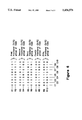
- FIG. 4 An example of such a distribution is illustrated in FIG. 4.
- an eight by eight switching matrix is shown which includes rows R1-R8 of input conductors and columns C1-C8 of output conductors. Binary numbers are superimposed on these rows and columns.
- Each binary number includes eight bits (four ones and four zeroes), each bit positioned at an intersection of a logical column and row. If the bit is a one, a physical switching device is available for connecting the column and the row at that intersection. If the binary bit is a zero, no switch is available for that intersection.
- rows R1 and R5 form a matching pair so that the binary number for row R5 is the complement of the binary number for row R1.
- rows R2 and R6, rows R3 and R7, and rows R4 and R8 form matching pairs with complementary binary numbers.
- binary numbers for the first third of the matrix input conductors are chosen in the same manner. As is shown in FIG. 5, the binary number chosen for each input conductor of the first group has one-third ones and two-thirds zeroes.
- the binary number chosen for each input conductor of the first group has one-third ones and two-thirds zeroes.
- a random number is selected for each input conductor in which the one-third of the ones may appear only where zeroes appear in the binary number of a selected (matching) one of the input conductors of the first third.
- Each input conductor of the second third is matched with an input conductor of the first third.
- the binary numbers for the last third are selected by providing ones in the columns where zeroes exist in both the matching row of the first third of input conductors and a matching row of the second third of input conductors. Again, a row of the first third, a row of the second third, and a row of the third third are matched to bring about this result.
- rows R1, R4, and R7 are matching rows
- rows R2, R5, and R8 are matching rows
- rows R3, R6, and R9 are matching rows.
- each of a first fraction of conductors is assigned binary numbers randomly where each such binary number includes a number of ones equal to the fraction of the total number of intersections which might be made in a full switch matrix.
- the second fractional group of conductors are assigned binary numbers randomly where each such number includes a number of ones equal to the fraction of the total of intersections which might be made in a full switch matrix, but the ones are allowed only in the columns where fewer ones than the numerator of the fraction reside in a matching one of the conductors of the first fraction of conductors.
- switching devices are furnished at each intersection where a one value occurs in the binary number assigned to each conductor to allow that conductor to connect to each intersecting conductor at such intersection.
- the input conductors are divided into five groups. For a first group of one fifth of the total of input conductors, random numbers are assigned to designate switching devices at two-fifths of the possible intersections for each input conductor of the group. Similarly, for a second group of one-fifth of the total of input conductors, random numbers are assigned to designate switching devices at two-fifths of the possible intersections for each input conductor of the group.
- random numbers are assigned to designate switching devices at two-fifths of the possible intersections for each input conductor of each group but only at intersections with an output conductor which has not yet been connected to two matching input conductors of groups previously assigned switching devices.
- the method for arranging switching devices in a switch matrix having a plurality of input conductors and a plurality of output conductors arranged as logically intersecting rows and columns, and where the switch matrix has a total number of switches which are a preset fraction of possible intersections between rows and columns, has a general step of assigning individual random binary numbers of ones and zeroes to each conductor of either the plurality of input conductors or the plurality of output conductors.
- Each such binary number assigned to a conductor has a number of bits which represent all of the possible intersections of the conductor which might be made with all conductors which the conductor intersects.
- the binary number assigned to each conductor includes binary ones substantially equal to the preset fraction of the total number of intersections which might be made with the conductor. The number need not be exact but should be close.
- the steps for carrying out the assignment start with assigning the conductors to which the random numbers are to be assigned into a number of groups, the number being equal to the denominator of the preset fraction. Then, the random binary numbers are assigned first to conductors of a first group of such conductors. Random binary numbers continue being assigned thereafter to conductors of additional groups of such conductors until all conductors of such groups have been assigned numbers.
- each additional group of conductors is matched to one conductor of each other group of conductors to which a binary number has been previously assigned.
- each such binary number assigned to a conductor of each additional group includes ones representing intersections with an intersecting conductor only where fewer ones than the numerator of the preset fraction reside in the corresponding position in the binary numbers assigned to the matching ones of the conductors of all previous groups of conductors. For example, in the two-fifths matrix described, a one may be assigned in a position in a binary number in which only one previous binary one was assigned for all matching conductors connecting to the intersecting conducting which the one represents.
- switching devices are furnished at each intersection where a one occurs in the binary number assigned to each conductor to allow that conductor to connect with each other conductor at such intersection.
- a switch matrix may be built which requires many fewer switching devices yet still allows the establishment of virtually all of the permissible combinations of connections in a shorter time than do prior art switch matrices.
- a switch matrix having 336 input conductors and 24 output conductors constructed using the above-described arrangement provides coverage of virtually all possible combinations of 24 input signals even though only half the number of switching devices are used. For example, we found in testing ten million random combinations that all but seven such combinations could be found in such a matrix.
- Constructing a fractional size switch matrix with a random distribution of the available switching devices ensures that a relatively large set of combinations of input conductors will be connectable to the output conductors, i.e., the coverage will be good. If the construction is not random, then the coverage may be very poor. For example, in a one-half size switch matrix, if all of the input conductors in the top half of the matrix have their switching devices in the same position and all of the input conductors in the bottom half of the matrix have their switching devices in the complementary positions, then the coverage will be minimal.
- the ones are summed in each of the selected input rows having a one at an intersection with the chosen column.
- the row having the least number of ones is selected. If more than one row has the same least number, any such row may be selected.
- the switch at the intersection of this first selected row and the first selected column is chosen for closure as a first step in providing the output combination desired.
- a smaller sub-matrix of rows including all of the input rows except the selected row and all of the columns except the selected column is selected.
- the ones in those columns are summed individually by columns, and the column having the least number of ones is selected.
- the ones in rows of this sub-matrix having ones at the intersections with the second chosen column are each summed. Again, the row having the least number of ones is selected.
- a switch at the intersection of this second selected row and the second selected column is chosen for closure as a next step in providing the output combination desired.
Landscapes
- Physics & Mathematics (AREA)
- Mathematical Physics (AREA)
- Engineering & Computer Science (AREA)
- Computer Hardware Design (AREA)
- Computing Systems (AREA)
- General Engineering & Computer Science (AREA)
- Computer Networks & Wireless Communication (AREA)
- Electronic Switches (AREA)
Abstract
Description
Claims (1)
Priority Applications (1)
| Application Number | Priority Date | Filing Date | Title |
|---|---|---|---|
| US08/246,731 US5436576A (en) | 1994-05-20 | 1994-05-20 | Switch matrices using reduced number of switching devices for signal routing |
Applications Claiming Priority (1)
| Application Number | Priority Date | Filing Date | Title |
|---|---|---|---|
| US08/246,731 US5436576A (en) | 1994-05-20 | 1994-05-20 | Switch matrices using reduced number of switching devices for signal routing |
Publications (1)
| Publication Number | Publication Date |
|---|---|
| US5436576A true US5436576A (en) | 1995-07-25 |
Family
ID=22931969
Family Applications (1)
| Application Number | Title | Priority Date | Filing Date |
|---|---|---|---|
| US08/246,731 Expired - Lifetime US5436576A (en) | 1994-05-20 | 1994-05-20 | Switch matrices using reduced number of switching devices for signal routing |
Country Status (1)
| Country | Link |
|---|---|
| US (1) | US5436576A (en) |
Cited By (14)
| Publication number | Priority date | Publication date | Assignee | Title |
|---|---|---|---|---|
| US5689686A (en) * | 1994-07-29 | 1997-11-18 | Cypress Semiconductor Corp. | Methods for maximizing routability in a programmable interconnect matrix having less than full connectability |
| US5716052A (en) * | 1994-09-12 | 1998-02-10 | Eg&G Pressure Science, Inc. | Pressure-energized sealing rings |
| US5848066A (en) * | 1994-08-01 | 1998-12-08 | Cypress Semiconductor Corp. | Methods for maximizing routability in a programmable interconnect matrix having less than full connectability |
| US6243664B1 (en) | 1998-10-27 | 2001-06-05 | Cypress Semiconductor Corporation | Methods for maximizing routability in a programmable interconnect matrix having less than full connectability |
| US6265895B1 (en) * | 1998-01-30 | 2001-07-24 | Altera Corporation | Programmable logic device incorporating a memory efficient interconnection device |
| WO2001054280A1 (en) * | 2000-01-21 | 2001-07-26 | Pageant Technologies, Inc. | Programmable array logic circuit employing non-volatile ferromagnetic memory cells |
| WO2001054279A1 (en) * | 2000-01-21 | 2001-07-26 | Pageant Technologies, Inc. | A register having a ferromagnetic memory cells |
| US6323678B1 (en) * | 1997-01-09 | 2001-11-27 | Fujitsu Limited | Integrated circuit device with programmable junctions and method of designing such integrated circuit device |
| US6362646B1 (en) * | 1997-06-20 | 2002-03-26 | Altera Corporation | Method and apparatus for reducing memory resources in a programmable logic device |
| US20040150008A1 (en) * | 2003-02-05 | 2004-08-05 | Alcatel | Electrical space switching matrix |
| US20040261048A1 (en) * | 2003-06-19 | 2004-12-23 | International Business Machines Corporation | Wire trimmed programmable logic array |
| US20070285127A1 (en) * | 2000-01-21 | 2007-12-13 | Estancia Limited | Programmable array logic circuit employing non-volatile ferromagnetic memory cells |
| US20110078645A1 (en) * | 2008-06-06 | 2011-03-31 | Shogo Nakaya | Circuit design system and circuit design method |
| US20240187000A1 (en) * | 2022-12-06 | 2024-06-06 | Abu Dhabi University | Programmable wiring system for reconfigurable devices |
Citations (6)
| Publication number | Priority date | Publication date | Assignee | Title |
|---|---|---|---|---|
| US4989022A (en) * | 1986-12-23 | 1991-01-29 | At&T Bell Laboratories | Rearrangeable multiconnection switching networks constructed using combinatorial designs |
| US5153463A (en) * | 1990-04-11 | 1992-10-06 | Kawasaki Steel Corporation | Programmable logic device having a reduced switching matrix |
| US5204556A (en) * | 1991-05-06 | 1993-04-20 | Lattice Semiconductor Corporation | Programmable interconnect structure for logic blocks |
| US5270974A (en) * | 1990-09-07 | 1993-12-14 | Alliance Semiconductor Corporation | Monolithic fail bit memory |
| US5327023A (en) * | 1991-03-28 | 1994-07-05 | Kawasaki Steel Corporation | Programmable logic device |
| US5371495A (en) * | 1992-01-24 | 1994-12-06 | Intel Corporation | Deterministic routing method for minimal switch circuits |
-
1994
- 1994-05-20 US US08/246,731 patent/US5436576A/en not_active Expired - Lifetime
Patent Citations (6)
| Publication number | Priority date | Publication date | Assignee | Title |
|---|---|---|---|---|
| US4989022A (en) * | 1986-12-23 | 1991-01-29 | At&T Bell Laboratories | Rearrangeable multiconnection switching networks constructed using combinatorial designs |
| US5153463A (en) * | 1990-04-11 | 1992-10-06 | Kawasaki Steel Corporation | Programmable logic device having a reduced switching matrix |
| US5270974A (en) * | 1990-09-07 | 1993-12-14 | Alliance Semiconductor Corporation | Monolithic fail bit memory |
| US5327023A (en) * | 1991-03-28 | 1994-07-05 | Kawasaki Steel Corporation | Programmable logic device |
| US5204556A (en) * | 1991-05-06 | 1993-04-20 | Lattice Semiconductor Corporation | Programmable interconnect structure for logic blocks |
| US5371495A (en) * | 1992-01-24 | 1994-12-06 | Intel Corporation | Deterministic routing method for minimal switch circuits |
Cited By (20)
| Publication number | Priority date | Publication date | Assignee | Title |
|---|---|---|---|---|
| US5923868A (en) * | 1994-07-29 | 1999-07-13 | Cypress Semiconductor Corp. | Methods for maximizing routability in a programmable interconnect matrix having less than full connectability |
| US5689686A (en) * | 1994-07-29 | 1997-11-18 | Cypress Semiconductor Corp. | Methods for maximizing routability in a programmable interconnect matrix having less than full connectability |
| US5848066A (en) * | 1994-08-01 | 1998-12-08 | Cypress Semiconductor Corp. | Methods for maximizing routability in a programmable interconnect matrix having less than full connectability |
| US5716052A (en) * | 1994-09-12 | 1998-02-10 | Eg&G Pressure Science, Inc. | Pressure-energized sealing rings |
| US6323678B1 (en) * | 1997-01-09 | 2001-11-27 | Fujitsu Limited | Integrated circuit device with programmable junctions and method of designing such integrated circuit device |
| US6362646B1 (en) * | 1997-06-20 | 2002-03-26 | Altera Corporation | Method and apparatus for reducing memory resources in a programmable logic device |
| US6265895B1 (en) * | 1998-01-30 | 2001-07-24 | Altera Corporation | Programmable logic device incorporating a memory efficient interconnection device |
| US6243664B1 (en) | 1998-10-27 | 2001-06-05 | Cypress Semiconductor Corporation | Methods for maximizing routability in a programmable interconnect matrix having less than full connectability |
| US20070285127A1 (en) * | 2000-01-21 | 2007-12-13 | Estancia Limited | Programmable array logic circuit employing non-volatile ferromagnetic memory cells |
| WO2001054280A1 (en) * | 2000-01-21 | 2001-07-26 | Pageant Technologies, Inc. | Programmable array logic circuit employing non-volatile ferromagnetic memory cells |
| WO2001054279A1 (en) * | 2000-01-21 | 2001-07-26 | Pageant Technologies, Inc. | A register having a ferromagnetic memory cells |
| US7463058B2 (en) | 2000-01-21 | 2008-12-09 | Estancia Limited | Programmable array logic circuit employing non-volatile ferromagnetic memory cells |
| US20040150008A1 (en) * | 2003-02-05 | 2004-08-05 | Alcatel | Electrical space switching matrix |
| US8305111B2 (en) * | 2003-02-05 | 2012-11-06 | Alcatel Lucent | Electrical space switching matrix |
| US7225422B2 (en) * | 2003-06-19 | 2007-05-29 | International Business Machines Corporation | Wire trimmed programmable logic array |
| US20040261048A1 (en) * | 2003-06-19 | 2004-12-23 | International Business Machines Corporation | Wire trimmed programmable logic array |
| US20110078645A1 (en) * | 2008-06-06 | 2011-03-31 | Shogo Nakaya | Circuit design system and circuit design method |
| US8640071B2 (en) * | 2008-06-06 | 2014-01-28 | Nec Corporation | Circuit design system and circuit design method |
| US20240187000A1 (en) * | 2022-12-06 | 2024-06-06 | Abu Dhabi University | Programmable wiring system for reconfigurable devices |
| US12244310B2 (en) * | 2022-12-06 | 2025-03-04 | Abu Dhabi University | Programmable wiring system for reconfigurable devices |
Similar Documents
| Publication | Publication Date | Title |
|---|---|---|
| US5436576A (en) | Switch matrices using reduced number of switching devices for signal routing | |
| EP0410759B1 (en) | Configurable logic array and method | |
| US3983538A (en) | Universal LSI array logic modules with integral storage array and variable autonomous sequencing | |
| US4506341A (en) | Interlaced programmable logic array having shared elements | |
| US3681757A (en) | System for utilizing data storage chips which contain operating and non-operating storage cells | |
| EP0099135B1 (en) | Dynamic gate array whereby an assembly of gates is simulated by logic operations on variables selected according to the gates | |
| US6122761A (en) | IC chip tester using compressed digital test data and a method for testing IC chip using the tester | |
| EP0160789B1 (en) | Test pattern generator | |
| US5764654A (en) | Semiconductor integrated circuit device having a test circuit | |
| US3996566A (en) | Shift and rotate circuit for a data processor | |
| EP0118704A1 (en) | Integrated circuit device and method of diagnosing the same | |
| JPH0378720B2 (en) | ||
| EP0126322B1 (en) | Testable array logic device | |
| US4074236A (en) | Memory device | |
| EP0266873A2 (en) | Programmable logic array | |
| US5572198A (en) | Method and apparatus for routing in reduced switch matrices to provide one hundred percent coverage | |
| US4327355A (en) | Digital device with interconnect matrix | |
| US5486766A (en) | Method for testing switch matrices | |
| JP3430231B2 (en) | Logic cell and semiconductor integrated circuit using the same | |
| EP0266874B1 (en) | Programmable logic array | |
| EP0469705B1 (en) | High speed testing for programmable logic devices | |
| US4864535A (en) | Entry point address circuit for microcode rom | |
| JP2953633B2 (en) | Test vector generator for logic IC testing machine | |
| JPS6330934A (en) | Element device and branch method for integrated circuit programmable sequence | |
| EP0199890A2 (en) | A self-sequencing logic circuit |
Legal Events
| Date | Code | Title | Description |
|---|---|---|---|
| AS | Assignment |
Owner name: INTEL CORPORATION, CALIFORNIA Free format text: ASSIGNMENT OF ASSIGNORS INTEREST;ASSIGNORS:HIBDON, GREGORY B.;INGRAM, JOHN M.;REEL/FRAME:007064/0102 Effective date: 19940705 |
|
| STCF | Information on status: patent grant |
Free format text: PATENTED CASE |
|
| CC | Certificate of correction | ||
| AS | Assignment |
Owner name: DELAWARE CAPITAL FORMATION, INC., DELAWARE Free format text: ASSIGNMENT OF ASSIGNORS INTEREST;ASSIGNOR:AUTOMATED TEST ENGINEERING, INC.;REEL/FRAME:009197/0991 Effective date: 19980508 |
|
| FEPP | Fee payment procedure |
Free format text: PAYOR NUMBER ASSIGNED (ORIGINAL EVENT CODE: ASPN); ENTITY STATUS OF PATENT OWNER: LARGE ENTITY |
|
| FPAY | Fee payment |
Year of fee payment: 4 |
|
| FPAY | Fee payment |
Year of fee payment: 8 |
|
| FPAY | Fee payment |
Year of fee payment: 12 |