US5394147A - Sequential conversion-type ADC using predetermined bits - Google Patents
Sequential conversion-type ADC using predetermined bits Download PDFInfo
- Publication number
- US5394147A US5394147A US08/033,215 US3321593A US5394147A US 5394147 A US5394147 A US 5394147A US 3321593 A US3321593 A US 3321593A US 5394147 A US5394147 A US 5394147A
- Authority
- US
- United States
- Prior art keywords
- bits
- register
- bit
- sequential conversion
- conversion
- Prior art date
- Legal status (The legal status is an assumption and is not a legal conclusion. Google has not performed a legal analysis and makes no representation as to the accuracy of the status listed.)
- Expired - Fee Related
Links
Images


Classifications
-
- H—ELECTRICITY
- H03—ELECTRONIC CIRCUITRY
- H03M—CODING; DECODING; CODE CONVERSION IN GENERAL
- H03M1/00—Analogue/digital conversion; Digital/analogue conversion
- H03M1/12—Analogue/digital converters
- H03M1/34—Analogue value compared with reference values
- H03M1/38—Analogue value compared with reference values sequentially only, e.g. successive approximation type
- H03M1/46—Analogue value compared with reference values sequentially only, e.g. successive approximation type with digital/analogue converter for supplying reference values to converter
- H03M1/462—Details of the control circuitry, e.g. of the successive approximation register
Definitions
- the present invention relates to sequential conversion-type A/D converters.
- this invention relates to sequential conversion-type ADCs with a control circuit for converting an analog input signal to a digital value, the control circuit proceeding sequentially from a leading bit through lower order bits of a sequential conversion register.
- FIG. 10 and FIG. 11 are diagrams of the configuration and key parts, respectively, of a conventional sequential A/D converter.
- FIG. 10 shows comparator 1 for comparing an analog input signal with the value of a D/A conversion result; sequential conversion register 2 for storing the result of A/D conversion and for decoding input data for a D/A converter; D/A converter 3 for converting the digital value (conversion result) of sequential conversion register 2 into an analog value; control circuit 4 for sequential conversion; and clock generator circuit 5 for A/D conversion.
- Analog input signal A, bit setting signals B supplied from control circuit 4 to sequential conversion register 2, one-bit conversion signal C, A/D conversion start signal D supplied from clock generator circuit 5 to both control circuit 4 and comparator 1, comparison voltage E output from D/A converter 3, and conversion complete signal F are also shown.
- latch circuit 6a for taking in data during a time interval "H" of an input clock signal (CLK) and latching data on the falling edge of the clock signal.
- Latch circuit 6a is set and reset by set signal S and reset signal R, respectively.
- latch circuit 6b for taking in data during a time interval "L” of the input clock signal and latching data on the rising edge of the clock signal.
- Latch circuits 6a and 6b constitute a shifter S.
- Bits 70 to 77 and 7S of shifters S (which form the control circuit 4) are arranged in order from high to low.
- Bit setting signals B7 to B0 are supplied to bits a7 to a0, respectively, of sequential conversion register 2 and correspond to bit setting signals B of FIG. 10.
- control circuit 4 is constructed of shifters S, each consisting of latch circuits 6a and 6b connected to each other in a cascade manner and forming each of bits 77 to 70 and 7S.
- A/D conversion start signal D becomes active at the start of A/D conversion, and shifter S of bit 77 of control circuit 4 is set.
- bit setting signal B7 becomes active in synchrony with a change in a one-bit conversion signal so that the leading bit a7 is set to "1" and bits a6 to a0 of sequential conversion register 2 are set to "0.”
- a digital value of sequential conversion register 2 is decoded into an analog value (comparison voltage E) by D/A converter 3.
- Comparison voltage E and analog input voltage A, input from outside, are compared by comparator 1 in response to one-bit conversion signal C.
- bit 77 at the start of conversion is shifted from bit 76 to bit 70 of shifters S in response to one-bit conversion signal C.
- bit a7 to bit a0 are sequentially set to "1.”
- Comparison between comparison voltage E output and decoded by D/A converter 3 and analog input voltage A is repeated for bits a7 to a0, and bits a7 to a0 are kept at "1" or cleared to "0". In this way, the value of each bit is determined, and a single A/D conversion result is obtained in sequential conversion register 2. Furthermore, when the data is shifted up to bit 7S, conversion complete signal F becomes active to complete conversion.
- Such a sequential conversion-type A/D converter is used to convert input data such as the water temperature of an engine radiator (TR), an engine boost pressure (BP), or car acceleration (MP) into digital signals.
- input data such as the water temperature of an engine radiator (TR), an engine boost pressure (BP), or car acceleration (MP) into digital signals.
- Such input data is selectively input into comparator 1 by clock generator circuit 5 as analog signal A for conversion into a digital signal.
- the present invention is intended to solve the above problem, and it is an object of the invention to achieve a sequential conversion-type A/D converter which can convert an analog input signal showing small changes in a shorter period of time than the conventional A/D converter, without compromising conversion accuracy.
- the sequential conversion-type A/D converter comprises a fixing bit register for identifying which bits of sequential conversion register 2 are to be fixed, a fixed value register for holding the binary values of the bits of the sequential conversion register to be fixed, and a conversion start position setting circuit for identifying a leading bit of a lower order than the bits of the sequential conversion register to be fixed.
- Control circuit 4 starts sequential conversion from a leading bit set by the conversion start position setting circuit.
- FIG. 1 is a diagram of the configuration of a sequential conversion-type A/D converter according to an embodiment of the invention.
- FIG. 2 is a diagram of a control circuit for sequential conversion according to the invention.
- FIG. 3 is a schematic diagram of a conversion start position setting circuit according to the invention.
- FIG. 4 is a schematic diagram of an inverter circuit according to the invention.
- FIG. 5 is a diagram of an all-bits-"1" detection circuit according to the invention.
- FIG. 6 is a diagram of an all-bits-"0" detection circuit according to the invention.
- FIG. 7 is a diagram of a sequential conversion-type A/D converter according to another embodiment of the invention.
- FIG. 8 is a diagram of the configuration of a sequential conversion-type A/D converter which consists of a four-input eight-bit A/D converter according to another embodiment of the invention.
- FIG. 9 is a diagram of a sequential conversion-type A/D converter according to another embodiment of the invention.
- FIG. 10 is a diagram of a conventional sequential conversion-type A/D converter.
- FIG. 11 is a diagram of the detailed configuration of the conventional sequential conversion-type A/D converter.
- FIG. 12 is a diagram of an analog input to be converted by the conventional A/D converter.
- FIG. 13 is a diagram of an analog input signal input into the conventional sequential conversion-type A/D converter.
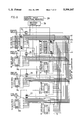
- FIGS. 1 to 6 are diagrams of the configuration of a sequential conversion-type A/D converter according to a preferred embodiment of the present invention.
- comparator 1 for comparing an analog input signal A and comparison voltage E from D/A converter 3; sequential conversion register 2 for storing the result of A/D conversion; D/A converter 3; control circuit 204 for sequential conversion; clock generator circuit 5 for A/D conversion; fixed value register 8 for setting fixed data values; fixing bit register 9 for identifying bits to be fixed; AND circuits 100 to 107 for generating signals for controlling the load of the fixed data into sequential conversion register 2 according to the values of fixing bit register 9 and in response to a conversion start signal; transmission gates 110 to 117; AND circuits 12 and 13; and detection circuits 14 and 15 for detecting whether all unfixed bits are "1" and "0", respectively.
- FIGS. 1-6 show comparison voltage E output from D/A converter 3; and conversion complete signal F.
- latch circuit 6a which can be set (S) and reset (R), for taking in data during a time interval "H" of an input clock signal and for latching data on the falling edge of the input clock signal; latch circuit 6b, for taking in data during a time interval "L” of the input clock signal and for latching data on the rising edge of the input clock signal; bits 77 to 70 and 7S of shifter S forming control circuit 204; and control signals B7 to B0 supplied to bits a7 to a0 of sequential conversion register 2 and corresponding to bit setting signals B of FIG. 1.
- AND circuits 16 to 23 decode the control signals for setting each bit of sequential conversion register 2 to "1" at the start of conversion.
- conversion start position setting signals e7 to e0 are "1"
- bits 77 to 70 are forcedly set at “1.”
- conversion start position setting signals e7 to e0 are output from AND circuits 16 to 23 which form conversion start position setting circuit 4M of FIG. 3. Inputs of predetermined combinations of bit signals d7 to d0 and their inverted signals of fixing bit register 9 are supplied to these AND circuits.
- bits d7, d6 and d5 are input to AND circuit 19.
- the inverted signals of bits d7 to d0 are generated from inverter circuits 16a to 16h shown in FIG. 4. Therefore, when bits d7 to d5 of fixing bit register 9 are set to "1," for example, only AND circuit 19 becomes active and only conversion start position setting signal e4 becomes "1,” so that sequential conversion starts from bit 74 of the shifter S.
- the A/D converter of the present invention comprises all-bits-"1" detection circuit 14 which consists of AND circuits 14b for obtaining the logical products of the inverted signal of bit d7 of fixing bit register 9 and bit a7, the inverted signal of bit d6 and bit a6, the inverted signal of bit d5 and bit a5, the inverted signal of bit d4 and bit a4, the inverted signal of bit d3 and bit a3, the inverted signal of bit d2 and bit a2, the inverted signal of bit d1 and bit al, and the inverted signal of bit d0 and bit a0; and AND circuit 12 for obtaining the logical product of the outputs of these AND circuits 14b.
- All-bits-"1" detection circuit 14 detects that all unfixed bits of sequential conversion register 2 are “1” and outputs all-bits-"1" detection signal IRQ1.
- the A/D converter further comprises the all-bits-"0" detection circuit 15 which consists of NOR circuits 15a for obtaining the logical sums of bit d7 of the fixing bit register 9 and bit a7, bit d6 and bit a6, bit d5 and bit a5, bit d4 and bit a4, bit d3 and bit a3, bit d2 and bit a2, bit d1 and bit a1, and bit d0 and bit a0; and AND circuit 13 for obtaining the logical sum of the outputs of these NOR circuits 15a.
- All-bits-"0" detection circuit 15 detects that all unfixed bits of sequential conversion register 2 are "0” and outputs all bits-"0" detection signal IRQ2.
- the operation of the A/D converter will be described. Since the A/D conversion of this embodiment of the present invention is of the sequential conversion type, its basic operation is the same as that of the prior art.
- the invention differs from the prior art in that, at the start of conversion, specified bits of sequential conversion register 2 are fixed at a specified value. The bit following the fixed bits is set to "1" to start conversion. That is, fixing bit data identifying which bits in the sequential conversion register are to be fixed and fixed value data for setting bits to be fixed to "1", for example, are set in fixing bit register 9 and fixed data register 8, respectively, to start A/D conversion.
- A/D conversion is performed, starting from the bit of sequential conversion register 2 corresponding to the bit of shifter S which has been set to "1" and proceeding through lower order bits by iterative conversion of one bit at a time, like the conventional A/D converter.
- the A/D converter of the present invention converts only bits of an order lower than the fixed bits.
- bits d7, d6 and d5 of fixing bit register 9 are set at “1". That is, bits d7 to d0 are set at “1", “1”, “1”, “0”, “0”, “0”, “0" and “0” and bits c7 to c5 of fixed value register 8 are set at “1", "0” and "0", respectively.
- bits a4 to a0 are sequential conversions performed by the unique operation of the control circuit 204 for sequential conversion.
- Bit a4 is first set to "1" to start conversion, and conversion up to bit a0 is performed to achieve a single conversion value.
- conversion time for an analog input signal which shows small changes as shown in FIG. 13 can be reduced, and the same accuracy of a conversion result from the prior art can be achieved.
- circuits 14 and 15 for detecting that all unfixed bits are "1" and "0", respectively it is possible to detect when an analog input voltage is outside the range of A/D conversion defined by the non-fixed bits.
- the detection signals from these circuits can be used as interrupt signals IRQ1 and IRQ2 to handle this case by interrupt processing.
- interrupt signals IRQ1 and IRQ2 are output from all-bits-"1" detection circuit 14 and all-bits-"0" detection circuit 15 when the analog input signal falls below the lower limit or goes beyond the upper limit of a predetermined range P, the process goes to an interrupt routine where an alarm lamp (not shown) is generated or an interrupt is generated to suspend the operation of the A/D converter in order to take a countermeasure.
- an IRQ interrupt signal
- the process enters an interrupt processing routine where the data of fixing bit register 9 and fixed value register 8 are reset and the variable range of an analog input is changed to continue conversion.
- the A/D converter comprises three pairs of fixing bit registers 9a to 9c and fixed value registers 8a to 8c for these three analog input signals. The appropriate pair of registers is selected according to the selected analog input signal.
- a four-input eight-bit A/D converter will be described with reference to FIG. 8 as an example for implementing this.
- This embodiment comprises first fixed value register 8a and first fixing bit register 9a for analog input signal A1 (TR), second fixed value register 8b and second fixing bit register 9b for analog input signal A2 (BP), third fixed value register 8c and third fixing bit register 9c for analog input signal A3 (MR), and fourth fixed value register 8d and fourth fixing bit register 9d for analog input signal A4.
- One pair consisting of a fixing bit register and a fixed value register for an analog input signal to be converted is selected, and conversion is performed on the data of the selected registers.
- four analog input signals A1 to A4 are connected to the respective analog inputs of the comparator through respective transmission gates 24 to 27.
- One of the analog inputs is selected by a control signal, obtained by decoding the data of analog input selection register 28 with decoder circuit 29, and supplied to the analog input of the comparator.
- a pair consisting of a fixing bit register and a fixed value register for the analog input selected by this selection signal is selected.
- signals (d07 to d00, c07 to c00) for supplying the data of the selected fixing bit register and the data of the selected fixed value register to each control circuit are supplied to each control circuit through each gate circuit G in place of the data (d7 to d0) of fixing bit register 9 and the data (c7 to c0) of fixed value register 8 of the above-mentioned embodiment (FIG. 1).
- a pair consisting of fixing bit register 9 and fixed value register 8 may be shared by a plurality of analog input signals TR1, TR2 and TR3, all of which have the same fluctuation width.
- the A/D converter comprises a fixing bit register for identifying bits in the sequential conversion register to be fixed, a fixed value register for setting bits to be fixed at "1" or "0", a conversion start position setting circuit for converting bits of a lower order than the bits of the sequential conversion register identified by the fixing bit register, and a control circuit for starting sequential conversion from a bit set by the conversion start position setting circuit, it is possible to reduce conversion time for analog input signals which show small changes and to achieve the same accuracy of a conversion result as the prior art.
- the A/D converter further comprises an all-bits-"0" detection circuit for detecting that the converted values of unfixed bits of the sequential conversion register are all "0” and an all-bits-"1" detection circuit for detecting that the converted values of unfixed bits of the sequential conversion register are all "1"
- an all-bits-"0" detection circuit for detecting that the converted values of unfixed bits of the sequential conversion register are all "0”
- an all-bits-"1 detection circuit for detecting that the converted values of unfixed bits of the sequential conversion register are all "1
Landscapes
- Engineering & Computer Science (AREA)
- Theoretical Computer Science (AREA)
- Analogue/Digital Conversion (AREA)
Abstract
Description
Claims (8)
Applications Claiming Priority (2)
| Application Number | Priority Date | Filing Date | Title |
|---|---|---|---|
| JP4-176071 | 1992-06-10 | ||
| JP4176071A JPH05343998A (en) | 1992-06-10 | 1992-06-10 | Sequential conversion type A / D converter |
Publications (1)
| Publication Number | Publication Date |
|---|---|
| US5394147A true US5394147A (en) | 1995-02-28 |
Family
ID=16007214
Family Applications (1)
| Application Number | Title | Priority Date | Filing Date |
|---|---|---|---|
| US08/033,215 Expired - Fee Related US5394147A (en) | 1992-06-10 | 1993-03-18 | Sequential conversion-type ADC using predetermined bits |
Country Status (3)
| Country | Link |
|---|---|
| US (1) | US5394147A (en) |
| JP (1) | JPH05343998A (en) |
| DE (1) | DE4311548C2 (en) |
Cited By (5)
| Publication number | Priority date | Publication date | Assignee | Title |
|---|---|---|---|---|
| US5870052A (en) * | 1995-02-24 | 1999-02-09 | Fujitsu Microelectronic Limited | Successive approximation type analog to digital converter with repetitive conversion cycles |
| US6076122A (en) * | 1996-10-01 | 2000-06-13 | Mitsubishi Electric Semiconductor Software Co., Ltd. | Microcomputer communicating analog-to-digital conversion results to central processing unit |
| US6761115B2 (en) * | 2001-05-07 | 2004-07-13 | Heidelberger Drunkmaschinen Ag | Clock generator for an imaging device using printing form angular position |
| US20050122247A1 (en) * | 2003-09-30 | 2005-06-09 | Infineon Technologies Ag | Analog-digital converter and method for analog-digital converting |
| US20100100248A1 (en) * | 2005-09-06 | 2010-04-22 | General Electric Company | Methods and Systems for Neural Network Modeling of Turbine Components |
Families Citing this family (5)
| Publication number | Priority date | Publication date | Assignee | Title |
|---|---|---|---|---|
| US5589832A (en) * | 1994-12-02 | 1996-12-31 | Lucent Technologies Inc. | Low noise non-sampled successive approximation |
| JP2010063055A (en) | 2008-09-08 | 2010-03-18 | Sony Corp | Successive approximation type a/d converter, successive approximation type a/d converter controlling method, solid-state imaging device, and image capturing apparatus |
| JP5263268B2 (en) * | 2010-11-10 | 2013-08-14 | ソニー株式会社 | Successive comparison type A / D converter and solid-state imaging device |
| JP6676983B2 (en) * | 2016-01-28 | 2020-04-08 | 株式会社リコー | Photoelectric conversion element, image reading device, image forming device, and image reading method |
| US9912346B1 (en) * | 2017-04-13 | 2018-03-06 | Ambiq Micro, Inc. | Digital-based power reduction technique for SAR ADCs |
Citations (4)
| Publication number | Priority date | Publication date | Assignee | Title |
|---|---|---|---|---|
| US4490713A (en) * | 1978-11-17 | 1984-12-25 | Burr-Brown Inc. | Microprocessor supervised analog-to-digital converter |
| US4764750A (en) * | 1986-06-19 | 1988-08-16 | Nec Corporation | Analog-to-digital converter |
| US5229770A (en) * | 1991-01-16 | 1993-07-20 | Mitsubishi Denki Kabushiki Kaisha | Analog/digital converter with advanced conversion termination notice |
| US5252976A (en) * | 1990-07-26 | 1993-10-12 | Fujitsu Limited | Sequential comparison type analog-to-digital converter |
Family Cites Families (2)
| Publication number | Priority date | Publication date | Assignee | Title |
|---|---|---|---|---|
| US4651132A (en) * | 1982-02-23 | 1987-03-17 | Burr-Brown Corporation | Analog to digital converter system for application to pulse code modulation |
| JPH02265326A (en) * | 1989-04-05 | 1990-10-30 | Nec Corp | Successive comparison type a/d converter |
-
1992
- 1992-06-10 JP JP4176071A patent/JPH05343998A/en active Pending
-
1993
- 1993-03-18 US US08/033,215 patent/US5394147A/en not_active Expired - Fee Related
- 1993-04-07 DE DE4311548A patent/DE4311548C2/en not_active Expired - Fee Related
Patent Citations (4)
| Publication number | Priority date | Publication date | Assignee | Title |
|---|---|---|---|---|
| US4490713A (en) * | 1978-11-17 | 1984-12-25 | Burr-Brown Inc. | Microprocessor supervised analog-to-digital converter |
| US4764750A (en) * | 1986-06-19 | 1988-08-16 | Nec Corporation | Analog-to-digital converter |
| US5252976A (en) * | 1990-07-26 | 1993-10-12 | Fujitsu Limited | Sequential comparison type analog-to-digital converter |
| US5229770A (en) * | 1991-01-16 | 1993-07-20 | Mitsubishi Denki Kabushiki Kaisha | Analog/digital converter with advanced conversion termination notice |
Cited By (8)
| Publication number | Priority date | Publication date | Assignee | Title |
|---|---|---|---|---|
| US5870052A (en) * | 1995-02-24 | 1999-02-09 | Fujitsu Microelectronic Limited | Successive approximation type analog to digital converter with repetitive conversion cycles |
| US6076122A (en) * | 1996-10-01 | 2000-06-13 | Mitsubishi Electric Semiconductor Software Co., Ltd. | Microcomputer communicating analog-to-digital conversion results to central processing unit |
| CN1123974C (en) * | 1996-10-01 | 2003-10-08 | 三菱电机半导体软件株式会社 | Microcomputer |
| US6761115B2 (en) * | 2001-05-07 | 2004-07-13 | Heidelberger Drunkmaschinen Ag | Clock generator for an imaging device using printing form angular position |
| US20050122247A1 (en) * | 2003-09-30 | 2005-06-09 | Infineon Technologies Ag | Analog-digital converter and method for analog-digital converting |
| US7079069B2 (en) | 2003-09-30 | 2006-07-18 | Infineon Technologies Ag | Analog-digital converter and method for analog-digital converting |
| US20100100248A1 (en) * | 2005-09-06 | 2010-04-22 | General Electric Company | Methods and Systems for Neural Network Modeling of Turbine Components |
| US8065022B2 (en) * | 2005-09-06 | 2011-11-22 | General Electric Company | Methods and systems for neural network modeling of turbine components |
Also Published As
| Publication number | Publication date |
|---|---|
| DE4311548C2 (en) | 1995-06-08 |
| JPH05343998A (en) | 1993-12-24 |
| DE4311548A1 (en) | 1993-12-16 |
Similar Documents
| Publication | Publication Date | Title |
|---|---|---|
| US5394147A (en) | Sequential conversion-type ADC using predetermined bits | |
| US5382955A (en) | Error tolerant thermometer-to-binary encoder | |
| US4454500A (en) | Analog data acquisition device | |
| CA1222826A (en) | Analog to digital converter | |
| US5859608A (en) | Successive approximation and shift register without redundancy | |
| US4520347A (en) | Code conversion circuit | |
| JPS6360569B2 (en) | ||
| US4553128A (en) | Analog-to-digital converter | |
| US6028545A (en) | Muti-bit successive-approximation analog-to-digital converter with improved conversion speed | |
| US5583503A (en) | Analog/digital converter | |
| JPH01131918A (en) | AD converter | |
| US6046692A (en) | Microprocessor equipped with an A/D converter | |
| US5969656A (en) | Digital-to-analog converter for increasing number of bits converted | |
| US5337050A (en) | Serial-to-parallel converter circuit | |
| JP2766133B2 (en) | Parallel-serial data conversion circuit | |
| US6617993B1 (en) | Analog to digital converter using asynchronously swept thermometer codes | |
| JP2771703B2 (en) | Single chip microcomputer | |
| US5920496A (en) | High speed correlator using up/down counter | |
| KR950004221B1 (en) | Data conversion method and circuit for performing the same | |
| JP3461672B2 (en) | Successive approximation A / D converter | |
| US4903027A (en) | A/D converter comprising encoder portion having function of multiplying analogue input by digital input | |
| JPH07231256A (en) | A/d converter | |
| JP2604740B2 (en) | Analog-to-digital converter | |
| US20040113825A1 (en) | High-speed oversampling modulator device | |
| SU1520506A1 (en) | Device for comparing numbers |
Legal Events
| Date | Code | Title | Description |
|---|---|---|---|
| AS | Assignment |
Owner name: MITSUBISHI DENKI KABUISHIKI KAISHA, JAPAN Free format text: ASSIGNMENT OF ASSIGNORS INTEREST.;ASSIGNOR:MIYAKE, TAKASHI;REEL/FRAME:006473/0704 Effective date: 19930311 |
|
| FEPP | Fee payment procedure |
Free format text: PAYOR NUMBER ASSIGNED (ORIGINAL EVENT CODE: ASPN); ENTITY STATUS OF PATENT OWNER: LARGE ENTITY |
|
| FPAY | Fee payment |
Year of fee payment: 4 |
|
| REMI | Maintenance fee reminder mailed | ||
| LAPS | Lapse for failure to pay maintenance fees | ||
| STCH | Information on status: patent discontinuation |
Free format text: PATENT EXPIRED DUE TO NONPAYMENT OF MAINTENANCE FEES UNDER 37 CFR 1.362 |
|
| FP | Lapsed due to failure to pay maintenance fee |
Effective date: 20030228 |
|
| AS | Assignment |
Owner name: CITICORP USA, INC., AS TERM C LOAN COLLATERAL AGEN Free format text: SECURITY AGREEMENT;ASSIGNOR:BREED AUTOMOTIVE TECHNOLOGY, INC.;REEL/FRAME:014428/0283 Effective date: 20030425 Owner name: CITICORP USA, INC., AS TERM C LOAN COLLATERAL AGENT AND CITICORP USA, INC. AS ADMINISTRATIVE AGENT, NEW YORK Free format text: SECURITY AGREEMENT;ASSIGNOR:BREED AUTOMOTIVE TECHNOLOGY, INC.;REEL/FRAME:014428/0283 Effective date: 20030425 |