US5367183A - Semiconductor device with complementary transistors - Google Patents
Semiconductor device with complementary transistors Download PDFInfo
- Publication number
- US5367183A US5367183A US08/043,553 US4355393A US5367183A US 5367183 A US5367183 A US 5367183A US 4355393 A US4355393 A US 4355393A US 5367183 A US5367183 A US 5367183A
- Authority
- US
- United States
- Prior art keywords
- type
- layer
- channel
- delta doped
- transistors
- Prior art date
- Legal status (The legal status is an assumption and is not a legal conclusion. Google has not performed a legal analysis and makes no representation as to the accuracy of the status listed.)
- Expired - Fee Related
Links
Images

Classifications
-
- H—ELECTRICITY
- H10—SEMICONDUCTOR DEVICES; ELECTRIC SOLID-STATE DEVICES NOT OTHERWISE PROVIDED FOR
- H10D—INORGANIC ELECTRIC SEMICONDUCTOR DEVICES
- H10D30/00—Field-effect transistors [FET]
- H10D30/40—FETs having zero-dimensional [0D], one-dimensional [1D] or two-dimensional [2D] charge carrier gas channels
- H10D30/47—FETs having zero-dimensional [0D], one-dimensional [1D] or two-dimensional [2D] charge carrier gas channels having two-dimensional [2D] charge carrier gas channels, e.g. nanoribbon FETs or high electron mobility transistors [HEMT]
- H10D30/471—High electron mobility transistors [HEMT] or high hole mobility transistors [HHMT]
- H10D30/475—High electron mobility transistors [HEMT] or high hole mobility transistors [HHMT] having wider bandgap layer formed on top of lower bandgap active layer, e.g. undoped barrier HEMTs such as i-AlGaN/GaN HEMTs
-
- H—ELECTRICITY
- H10—SEMICONDUCTOR DEVICES; ELECTRIC SOLID-STATE DEVICES NOT OTHERWISE PROVIDED FOR
- H10D—INORGANIC ELECTRIC SEMICONDUCTOR DEVICES
- H10D62/00—Semiconductor bodies, or regions thereof, of devices having potential barriers
- H10D62/60—Impurity distributions or concentrations
- H10D62/605—Planar doped, e.g. atomic-plane doped or delta-doped
-
- H—ELECTRICITY
- H10—SEMICONDUCTOR DEVICES; ELECTRIC SOLID-STATE DEVICES NOT OTHERWISE PROVIDED FOR
- H10D—INORGANIC ELECTRIC SEMICONDUCTOR DEVICES
- H10D84/00—Integrated devices formed in or on semiconductor substrates that comprise only semiconducting layers, e.g. on Si wafers or on GaAs-on-Si wafers
- H10D84/01—Manufacture or treatment
- H10D84/02—Manufacture or treatment characterised by using material-based technologies
- H10D84/05—Manufacture or treatment characterised by using material-based technologies using Group III-V technology
Definitions
- the present invention relates to a semiconductor device comprising at least two complementary type transistors formed around a heterostructure of junctions between materials of the III-V groups.
- One of the particular features of this device is that its structure can be used to balance the threshold voltages V T of the two transistors, which are n and p type transistors, and to optimize their mutual conductance or transconductance values, despite the differences in mobility between the electrons and the holes.
- One of the objects of this device is to reduce the electrical consumption of the fast logic circuits and of the microwave circuits.
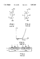
- the basic cell in logic circuits is the inverter, as shown in FIG. 1.
- This DCFL (Direct Coupled FET Logic) type inverter is formed by an enhanced n type input transistor 1, series-connected with a depleted n type active load 2, the entire unit being supplied between the ground and a voltage V DD .
- the input signal is applied at I on the gate of the transistor 1 and the output signal is collected at O on the drain of the same transistor.
- the power consumed (0.3, 1 mW) by this basic inverter: ##EQU1## is proportional to the working frequency (kf) but comprises a constant term corresponding to the consumption of the active load 2, even if the inverter is idle.
- BFL Bitered Fet Logic
- HIGFET Heterostructure Insulated Gate Fet
- heterostructure field-effect transistors one of them with one n channel and the other with one p channel.
- the heterostructure i.e., by definition, one or more junctions between two or more layers of different materials of the III-V group, for example GaAs and GaInAs
- TEGFETs or HEMTs High Electron Mobility Transistors
- HIGFETs have an excellent uniformity of threshold voltage V T on a wafer, during manufacture. This threshold voltage depends very little on the temperature and shows little sensitivity to light because it is not controlled by dopants.
- a first drawback of HIGFETs in their known structures, is that the two transistors, n and p, have different threshold voltages, in terms of absolute value, which is not suited to logic operations since the logic pulses (the bits) must have the same amplitude irrespectively of the transistor that is in operation.
- a second drawback of known HIGFETs is the difference in transconductance between the two channels which is of the order of 218 mS/mm for the n channel and 28 mS/mm for the p channel, at ambient temperature in both cases. This difference can be explained notably by the low mobility of the holes ⁇ h at ambient temperature.
- the invention proposes a new structure for a semiconductor device comprising at least two heterostructure transistors constituted by junctions between materials of the III-V group, at least one of these transistors having an n type channel, with electrons, and at least another transistor having a p type channel, with holes.
- This structure is characterized by the presence of a recess obtained by etching, in the region of the n channel, and by the fact that the n and p type transistors are made independently, thus enabling them to be adjusted separately.
- Another object of the invention is to optimize the threshold voltages V Tn and V Tp independently, by means of at least two delta doped layers, one of which is included in the surface layer that has been spared in the etching of the recess.
- Another object of the invention is to symmetrize and improve the ratio of the transconductance values.
- Another object of the invention is to enable the logic ports to work at a low supply voltage V DD ( ⁇ 1 V) without any lowering of performance characteristics. This enables the logic circuit to have greater complexity without excessive consumption because the gate currents are negligible.
- Another object of the invention is to have available a semiconductor device for which the method of manufacture, and in particular the selective etching, is compatible with presently used methods for the industrial-scale manufacture of field-effect transistors for VLSI circuits.
- the invention relates to a semiconductor device using complementary transistors, comprising at least two field-effect transistors made by means of a heterostructure of layers of semiconductor materials of the III-V group, at least one of these transistors having an n type channel (2DEG) and at least one other transistor having a p type channel (2DHG), these two channels being located at the same heterojunction in the heterostructure, wherein said device comprises, in two distinct layers of the heterostructure, at least two delta doped layers located between the channels (2DEG and 2DHG) and the gate metallizations of the transistors, the first of these delta doped layers being a p type layer and the second being an n type layer.
- complementary transistors comprising at least two field-effect transistors made by means of a heterostructure of layers of semiconductor materials of the III-V group, at least one of these transistors having an n type channel (2DEG) and at least one other transistor having a p type channel (2DHG), these two channels being located at the same heterojunction in the heterostructure, wherein said device
- FIG. 1 shows an electrical diagram of an inverter according to the prior art
- FIG. 2 shows an electrical diagram of an inverter in a complementary logic configuration that is known but is however, that of the-device according to the invention
- FIG. 4 shows a sectional view of an integrated circuit comprising an n type HIGFET and an p type HIGFET according to the prior art
- FIG. 5 shows a sectional view of an integrated circuit comprising two heterostructure transistors with n channels and p channels, according to the invention.
- FIG. 2 shows the electrical diagram of an inverter, or complementary logic circuit, according to the invention: it comprises two enhanced circuits 3 and 4, series-connected between a supply V DD and the ground, one of the transistors 3 having an n channel and the other having a p channel.
- This inverter and the DCFL type inverter is that the input signal is applied simultaneously to both gates of both transistors 3 and 4.
- This diagram is not different from that of a complementary MOS pair: the whole difficulty is to set it up with III-V materials to make a fast logic circuit, whereas C-MOS transistors on silicon are reputed to be slow.
- the threshold voltage V T should be substantially equal, in terms of absolute value, to the maximum gate-source voltage
- the voltage V GSmax is shown in FIG. 3: it is of the order of 0.6 V for the MESFETs and 1 V for the TEGFETs or HEMTs.
- This voltage which is dictated by the height of the barrier of the Schottky gate of a transistor, is the voltage beyond which there is a leakage of current through the gate.
- the maximum gate voltage pulse is limited by the gate leakage current which therefore reduces also the noise margin.
- the gate leakage current leads to a decrease in the drain saturation current, thus reducing the maximum speed of operation of the system.
- the factor 1/5 is chosen arbitrarily, for the logic excursion cannot be less than V T (it has no effect on the transistor) but should not be greater than V GSmax .
- a second major condition is that these two threshold voltages should be substantially equal in terms of absolute value, so as to symmetrize the working of the inverter.
- FIG. 4 shows a sectional view of an integrated circuit comprising an n type HIGFET and a p type HIGFET described in IEEE EDL, vol. ED1, vol. EDL 6, No. 12, December 1985, pp. 645 ff.
- a substrate 5 of non-intentionally doped (nid) GaAs a layer 6 of non-intentionally doped AlGaAs 6 is made to grow: there is therefore a heterojunction between two different semi-insulator materials.
- Gate metallizations 7 and 8 which are WSi refractories, are deposited before two implantations which create n doped self-aligned regions about one gate and other p doped self-aligned regions about another gate (8).
- n + and p + overdoping enable the deposition of the source and drain ohmic contacts 9 and 10 on the n type transistor and 11 and 12 on the p type transistor.
- the implantations are deep enough to reach the level of the heterojunction: therefore all the conditions have been assembled to have a 2D electron gas (2DEG) as an n channel and a 2D hole gas (2DHG) as a p channel.
- 2DEG and 2DHG are used by convention in international scientific literature).
- V GSmax ⁇ 1 V for an HEMT If V GSmax ⁇ 1 V for an HEMT, the excursion necessary for the generation of current V GSmax -V T ⁇ 0.3/0.35 V is low, and the logic is relatively slow.
- a first improvement consists in making the 2DEG and 2DHG channels of the two transistors out of a material of the III-V group having a smaller gap than that of GaAs, for example InGaAs instead of GaAs which improves the p channel transistor:
- a second improvement provided by the invention consists in introducing front delta doped layers, i.e. between the gate and the channel.
- the technique of the delta doped layer or doped plane is known per se: it consists in introducing a doping impurity (silicon or beryllium for example) during the epitaxial growth of a non-doped layer of semiconductor material localized in a film having a thickness of a few atoms, buried in a non-doped layer.
- a doping impurity silicon or beryllium for example
- the single delta doped layer is a rear layer, i.e. it is between the channel and the substrate, and the threshold voltages are given by the equations:
- ⁇ is the electrical charge per unit of area of the delta doped layer
- d is the distance from the channel to the gate.
- the second improvement provided by the invention consists in the introduction of at least two front delta doped layers, between the channel and the gate metallization, thus enabling the optimizing of the two threshold voltages V Tn and V Tp by means of two doping agents, each at the necessary doping level: these two delta doping layers are not merged in a same geometrical plane but are superimposed, thus enabling one of them to be isolated by localized etching.
- FIG. 5 shows a sectional view of the device with two n and p type complementary transistors according to the invention.
- the references common with those of the previously described transistors of FIG. 4 have been kept in this figure.
- the materials and the number of layers are given therein purely by way of a non-restrictive example.
- a substrate 5 made of semi-insulating GaAs the following are made to grow successively by epitaxy:
- a GaAs layer 18 with a thickness of 100 ⁇ , comprising a delta doped layer ⁇ n at 20.
- a selective and localized RIE etching of the layer 18 enables the elimination of the n type delta doped layer 20 above the future p type transistor, thus making V Tn and V Tp independent. This etching comes into play as soon as the manufacturing method starts.
- the delta doped layer 19 is designed to adjust V Tp . It is located approximately at mid-thickness in the GaAs layer 16, at a distance d p from the plane of the gate 8 of the p channel transistor. The charge ⁇ p is set, by the dose of the delta doping, to obtain the desired V Tp .
- the delta doped layer 20 is designed to adjust V Tn . It is located at a distance d nn from the plane of the gate 7 of the n channel transistor.
- the setting of the charge ⁇ n must take account of the fact that this n channel transistor furthermore comprises the delta doped layer 19 with a charge ⁇ .
- each of these doping layers can be replaced by two or more layers 19a, 19b, 19c. . . and 20a, 20b, 20c. . . for the technique for this is very simple; the only condition is that all the layers of a given type should the same values of ⁇ n d n or ⁇ p d p as a single layer of theme type, 19 or 20.
- n + and p + type contact wells that adjoin the 2DEG and 2DHG channels are made by implantations with self-alignment on the gates 7 and 8 made of WSi, then the ohmic contacts 9 to 12 are deposited, according to the well-known methods for the industrial-scale manufacture of MESFETs.
- d 1 2DEG channel/gate 7 distance (n type transistor)
- d 2 2DHG channel/gate 8 distance (p type transistor)
- V Tp the threshold voltage V Tp is defined by:
- V° Tp ⁇ -0.38 V is the threshold voltage without delta doped layer 19.
- the delta doped layer 19 is made by Be doping.
- V Tn the threshold voltage V Tn
- V° Tn ⁇ +0.78 V is the threshold voltage without the delta doped layers 19 and 20.
- the doped layer 20 is made by means of Si.
- the use of two front delta doped layers i.e. layers located between the gate and the channel, conjugated with a selective etching that partially eliminates one of these doping layers, enables the making of an inverter with complementary field-effect transistors, made of III-V type materials for fast logic operation.
- the elimination, by etching, of one of the two delta doped layers enables the independent optimizing of the two threshold voltages as well as the independent optimizing of the transconductance g m of the two transistors.
- These transistors can work with a low supply voltage V DD ( ⁇ 1 V) without deterioration of the performance characteristics, because V GS max ⁇ 1 V has been chosen.
- the low threshold voltages permit high logic excursion, the result of which is that the transistor has a capacity to give more current during the transients, and high performance characteristics during changes in state: T pd ⁇ 50 ps.
- the device according to the invention can be made with any of the compounds of the III-V group (Al, Ga, In, P, As) in the form of binary, ternary or quaternary alloys, if these compounds form two n channel and p channel heterojunction transistors, comprising at least two "front" delta doped layers, according to the spirit of the invention, which is specified in the following claims.
- III-V group Al, Ga, In, P, As
Landscapes
- Junction Field-Effect Transistors (AREA)
Abstract
Disclosed is a system with at least two complementary transistors, having n and p channels but comprising a heterostructure of junctions between III-V group materials. In order to balance the threshold voltages in the two channels, namely the n (2DEG) and p (2DHG) channels, at least two p and n delta doped layers are included in two layers of the heterostructure, at levels included between the channels (2DEG, 2DHG) and the gate electrodes. The n delta doped layer is then removed by localized etching right above the p channel transistor. Application to fast logic circuits.
Description
1. Field of the Invention
The present invention relates to a semiconductor device comprising at least two complementary type transistors formed around a heterostructure of junctions between materials of the III-V groups. One of the particular features of this device is that its structure can be used to balance the threshold voltages VT of the two transistors, which are n and p type transistors, and to optimize their mutual conductance or transconductance values, despite the differences in mobility between the electrons and the holes.
One of the objects of this device is to reduce the electrical consumption of the fast logic circuits and of the microwave circuits.
2. Description of the Prior Art
It is known that, in fast logic circuits, to date it is only n type transistors that are used because, in the channel, the electrons have far higher mobility than the holes, giving the transistors a higher cut-off frequency.
It is also known that the basic cell in logic circuits is the inverter, as shown in FIG. 1. This DCFL (Direct Coupled FET Logic) type inverter is formed by an enhanced n type input transistor 1, series-connected with a depleted n type active load 2, the entire unit being supplied between the ground and a voltage VDD. The input signal is applied at I on the gate of the transistor 1 and the output signal is collected at O on the drain of the same transistor. The power consumed (0.3, 1 mW) by this basic inverter: ##EQU1## is proportional to the working frequency (kf) but comprises a constant term corresponding to the consumption of the active load 2, even if the inverter is idle.
The use of a BFL (Buffered Fet Logic) inverter is even more characteristic for, apart from the fact that the transistors are all depletion transistors, the inverter of FIG. 1 is followed by a shifting stage which also consumes power in the idle state, which means that the power consumed is of the order of 5 to 10 mW.
Furthermore, it is known that complementary MOS transistors, on silicon, have the advantage of zero consumption when idle and have consumption proportional to the frequency (kf) when working. This is why, for fast logic systems (corresponding to operation at microwave frequencies in the gigahertz range), it is desirable to have a device comparable to MOS transistors, which are presently limited to about 1 to 3 GHz.
Circuits have been made on the basis of this principle, using two HIGFET (Heterostructure Insulated Gate Fet) transistors or heterostructure field-effect transistors, one of them with one n channel and the other with one p channel. The heterostructure (i.e., by definition, one or more junctions between two or more layers of different materials of the III-V group, for example GaAs and GaInAs) is promising because it is one of the bases (among others) of the fast transistors known as TEGFETs or HEMTs (High Electron Mobility Transistors) and because HIGFETs have an excellent uniformity of threshold voltage VT on a wafer, during manufacture. This threshold voltage depends very little on the temperature and shows little sensitivity to light because it is not controlled by dopants.
A first drawback of HIGFETs, in their known structures, is that the two transistors, n and p, have different threshold voltages, in terms of absolute value, which is not suited to logic operations since the logic pulses (the bits) must have the same amplitude irrespectively of the transistor that is in operation.
A second drawback of known HIGFETs is the difference in transconductance between the two channels which is of the order of 218 mS/mm for the n channel and 28 mS/mm for the p channel, at ambient temperature in both cases. This difference can be explained notably by the low mobility of the holes μh at ambient temperature.
The invention proposes a new structure for a semiconductor device comprising at least two heterostructure transistors constituted by junctions between materials of the III-V group, at least one of these transistors having an n type channel, with electrons, and at least another transistor having a p type channel, with holes. This structure is characterized by the presence of a recess obtained by etching, in the region of the n channel, and by the fact that the n and p type transistors are made independently, thus enabling them to be adjusted separately.
Another object of the invention is to optimize the threshold voltages VTn and V Tp independently, by means of at least two delta doped layers, one of which is included in the surface layer that has been spared in the etching of the recess.
Another object of the invention is to symmetrize and improve the ratio of the transconductance values.
Another object of the invention is to enable the logic ports to work at a low supply voltage VDD (˜1 V) without any lowering of performance characteristics. This enables the logic circuit to have greater complexity without excessive consumption because the gate currents are negligible.
Another object of the invention is to have available a semiconductor device for which the method of manufacture, and in particular the selective etching, is compatible with presently used methods for the industrial-scale manufacture of field-effect transistors for VLSI circuits.
More specifically, the invention relates to a semiconductor device using complementary transistors, comprising at least two field-effect transistors made by means of a heterostructure of layers of semiconductor materials of the III-V group, at least one of these transistors having an n type channel (2DEG) and at least one other transistor having a p type channel (2DHG), these two channels being located at the same heterojunction in the heterostructure, wherein said device comprises, in two distinct layers of the heterostructure, at least two delta doped layers located between the channels (2DEG and 2DHG) and the gate metallizations of the transistors, the first of these delta doped layers being a p type layer and the second being an n type layer.
The invention will be understood more clearly from the following description of an exemplary application, made with reference So the appended drawings, of which:
FIG. 1 shows an electrical diagram of an inverter according to the prior art;
FIG. 2 shows an electrical diagram of an inverter in a complementary logic configuration that is known but is however, that of the-device according to the invention;
FIG. 3 shows a characteristic where IG =f (VGS),
FIG. 4 shows a sectional view of an integrated circuit comprising an n type HIGFET and an p type HIGFET according to the prior art;
FIG. 5 shows a sectional view of an integrated circuit comprising two heterostructure transistors with n channels and p channels, according to the invention.
FIG. 2 shows the electrical diagram of an inverter, or complementary logic circuit, according to the invention: it comprises two enhanced circuits 3 and 4, series-connected between a supply VDD and the ground, one of the transistors 3 having an n channel and the other having a p channel. The difference between this inverter and the DCFL type inverter is that the input signal is applied simultaneously to both gates of both transistors 3 and 4. This diagram is not different from that of a complementary MOS pair: the whole difficulty is to set it up with III-V materials to make a fast logic circuit, whereas C-MOS transistors on silicon are reputed to be slow.
Indeed, if the consumption for this pair of transistors 3 and 4 is zero in static mode and proportional to the frequency in dynamic mode (kf), then there are at least two major conditions for the two types of transistors.
First of all, the threshold voltage VT should be substantially equal, in terms of absolute value, to the maximum gate-source voltage
|V.sub.T |≃1/5|V.sub.GS max |
The voltage VGSmax is shown in FIG. 3: it is of the order of 0.6 V for the MESFETs and 1 V for the TEGFETs or HEMTs. This voltage, which is dictated by the height of the barrier of the Schottky gate of a transistor, is the voltage beyond which there is a leakage of current through the gate. The maximum gate voltage pulse is limited by the gate leakage current which therefore reduces also the noise margin. Furthermore, the gate leakage current leads to a decrease in the drain saturation current, thus reducing the maximum speed of operation of the system.
The factor 1/5 is chosen arbitrarily, for the logic excursion cannot be less than VT (it has no effect on the transistor) but should not be greater than VGSmax.
This enables a logic excursion of 4/5 VGSmax for each transistor (n and p) to which there corresponds a saturation current of:
I.sub.Dmax =f(4/5 V.sub.GSmax)
Furthermore, a second major condition is that these two threshold voltages should be substantially equal in terms of absolute value, so as to symmetrize the working of the inverter.
Another condition, which may be resolved independently, is that these two threshold voltages should be substantially equal in terms of absolute value, so as to symmetrize the working of the inverter.
Another condition, which can be resolved independently, is that the transconductance values should be substantially equal.
FIG. 4 shows a sectional view of an integrated circuit comprising an n type HIGFET and a p type HIGFET described in IEEE EDL, vol. ED1, vol. EDL 6, No. 12, December 1985, pp. 645 ff. On a substrate 5 of non-intentionally doped (nid) GaAs, a layer 6 of non-intentionally doped AlGaAs 6 is made to grow: there is therefore a heterojunction between two different semi-insulator materials. Gate metallizations 7 and 8, which are WSi refractories, are deposited before two implantations which create n doped self-aligned regions about one gate and other p doped self-aligned regions about another gate (8). Contact regions with n+ and p+ overdoping enable the deposition of the source and drain ohmic contacts 9 and 10 on the n type transistor and 11 and 12 on the p type transistor. The implantations are deep enough to reach the level of the heterojunction: therefore all the conditions have been assembled to have a 2D electron gas (2DEG) as an n channel and a 2D hole gas (2DHG) as a p channel. (The abbreviations 2DEG and 2DHG are used by convention in international scientific literature).
The drawback of this system, which is otherwise very simple, is that for the pair GaAs/Alx GaI-x As, with x=0.3
V.sub.Tn ≃+0,78 V
V.sub.Tp ≃-0,65 V
If VGSmax ≈1 V for an HEMT, the excursion necessary for the generation of current VGSmax -VT ≈0.3/0.35 V is low, and the logic is relatively slow.
A first improvement consists in making the 2DEG and 2DHG channels of the two transistors out of a material of the III-V group having a smaller gap than that of GaAs, for example InGaAs instead of GaAs which improves the p channel transistor:
V.sub.Tp =-0,38 V
but does not modify the n channel transistor
V.sub.Tn =+0,78 V
To balance the threshold voltages and distribute the gain obtained between the two types of transistors, a second improvement provided by the invention consists in introducing front delta doped layers, i.e. between the gate and the channel.
The technique of the delta doped layer or doped plane is known per se: it consists in introducing a doping impurity (silicon or beryllium for example) during the epitaxial growth of a non-doped layer of semiconductor material localized in a film having a thickness of a few atoms, buried in a non-doped layer.
In the known cases, the single delta doped layer is a rear layer, i.e. it is between the channel and the substrate, and the threshold voltages are given by the equations:
V.sub.Tn =φ.sub.m -ΔE.sub.c -(σ/ε) d
V.sub.Tp =φ.sub.m -ΔE.sub.c -.sub.g2 -(σ/ε)d
in which:
σ is the electrical charge per unit of area of the delta doped layer;
εis the dielectric permittivity;
d is the distance from the channel to the gate.
It is then possible to choose the nature of the doping and the charge σ so that the threshold voltages are equal in terms of absolute value.
|V.sub.Tn |=|V.sub.Tp |≃1/2V.sub.GSmax ≃0,5V
but this approach leads to a low-speed operation of the logic circuit because the logic excursion 1/2VGSmax is smaller than the desired excursion of 4/5 V GSmax.
Increasing the supply voltage VDD to increase the flip-over speed of the transistor is not a suitable solution because, beyond about 1.25 V, the Schottky gate barrier is crossed and there is an increase in static consumption by leakage through the gate.
This is why the second improvement provided by the invention, referred to further above, consists in the introduction of at least two front delta doped layers, between the channel and the gate metallization, thus enabling the optimizing of the two threshold voltages VTn and VTp by means of two doping agents, each at the necessary doping level: these two delta doping layers are not merged in a same geometrical plane but are superimposed, thus enabling one of them to be isolated by localized etching.
FIG. 5 shows a sectional view of the device with two n and p type complementary transistors according to the invention. The references common with those of the previously described transistors of FIG. 4 have been kept in this figure. The materials and the number of layers are given therein purely by way of a non-restrictive example.
On a substrate 5 made of semi-insulating GaAs, the following are made to grow successively by epitaxy:
1) a buffer layer or smoothing layer 13 made of non-intentionally doped GaAs, on a thickness of 5000 Å;
2) a layer 14 of Inx Ga1-x As (x≈0.25), with a thickness of about 150 Å, in which there is developed either a 2DEG (electron gas) or a 2DHG (hole gas) with heterojunction with the next layer;
3) a layer 15 of Alx Gai-x As (x≈0.75) on a thickness of 100 Å;
4) A GaAs layer 16, with a thickness of 50 Å, comprising a delta doped layer σp which shall be referred to again further below,
5) A layer 17 of Aly Ga1-y As (y≈0.3) which
simultaneously constitutes a barrier layer for the selective etching of GaAs and a barrier layer with a thickness of 50 Å for the p channel transistor,
6) a GaAs layer 18, with a thickness of 100 Å, comprising a delta doped layer σn at 20.
After the epitaxial growth of all these layers, a selective and localized RIE etching of the layer 18 enables the elimination of the n type delta doped layer 20 above the future p type transistor, thus making VTn and VTp independent. This etching comes into play as soon as the manufacturing method starts.
The delta doped layer 19 is designed to adjust VTp. It is located approximately at mid-thickness in the GaAs layer 16, at a distance dp from the plane of the gate 8 of the p channel transistor. The charge σp is set, by the dose of the delta doping, to obtain the desired VTp.
The delta doped layer 20 is designed to adjust VTn. It is located at a distance dnn from the plane of the gate 7 of the n channel transistor. The setting of the charge σn must take account of the fact that this n channel transistor furthermore comprises the delta doped layer 19 with a charge σ.
In order to simplify FIG. 5, only two delta doped layers 19 and 20 have been shown. It is clear to those skilled in the art that each of these doping layers can be replaced by two or more layers 19a, 19b, 19c. . . and 20a, 20b, 20c. . . for the technique for this is very simple; the only condition is that all the layers of a given type should the same values of σn dn or σp dp as a single layer of theme type, 19 or 20.
The n+ and p+ type contact wells that adjoin the 2DEG and 2DHG channels are made by implantations with self-alignment on the gates 7 and 8 made of WSi, then the ohmic contacts 9 to 12 are deposited, according to the well-known methods for the industrial-scale manufacture of MESFETs.
The described structure, in which the n type doping layer 20 is above the p type doping layer 19, is preferable to a reverse structure. Indeed, according to the structure described, we have:
d.sub.1 >d.sub.2
with
d1 =2DEG channel/gate 7 distance (n type transistor) d2 =2DHG channel/gate 8 distance (p type transistor)
The enables partial compensation for the mobility of the holes which is lower than the mobility of the electrons.
For the p channel transistor (2DHG) which has only one delta doped layer 19, the threshold voltage VTp is defined by:
V.sub.Tp =V°.sub.Tp +(|σpVε)d.sub.p
where V°Tp ≈-0.38 V is the threshold voltage without delta doped layer 19.
To obtain:
V.sub.Tp ≃1/5 V.sub.GS max ≃-0,2V
which is a desired value so that the logic excursion is 4/5 V GSmax, and with dp =70 Å(50 Å in the layer 17+20 Å in the layer 16), the surface density is computed
D.sub.p ≃1,4.10.sup.12 at.cm.sup.-2
The delta doped layer 19 is made by Be doping.
For the n channel transistor (2DEG), with two delta doped layers 19 and 20, the threshold voltage VTn is defined by:
V.sub.Tn =V°.sub.Tn -(σ.sub.n /ε)d.sub.n +(|σ.sub.p |/ε)d.sub.p
wherein V°Tn ≈+0.78 V is the threshold voltage without the delta doped layers 19 and 20.
σp is already determined by the computation of VTp : to obtain
D.sub.n ≃7.10.sup.12 at.cm.sup.-2
which symmetrizes the logic inverter, and with dn ≈90 Å, it is found that:
V.sub.Tn ≃1/5 V.sub.GS max ≃+0,2 V
The doped layer 20 is made by means of Si.
Thus, the use of two front delta doped layers, i.e. layers located between the gate and the channel, conjugated with a selective etching that partially eliminates one of these doping layers, enables the making of an inverter with complementary field-effect transistors, made of III-V type materials for fast logic operation. Indeed, the elimination, by etching, of one of the two delta doped layers enables the independent optimizing of the two threshold voltages as well as the independent optimizing of the transconductance gm of the two transistors.
These transistors can work with a low supply voltage VDD (˜1 V) without deterioration of the performance characteristics, because VGS max<1 V has been chosen. The low threshold voltages permit high logic excursion, the result of which is that the transistor has a capacity to give more current during the transients, and high performance characteristics during changes in state: Tpd <50 ps.
The invention has been described with reference to an example in which the compositions and the thicknesses of the layers are mentioned solely in order to simplify the explanation. It is clear that the device according to the invention can be made with any of the compounds of the III-V group (Al, Ga, In, P, As) in the form of binary, ternary or quaternary alloys, if these compounds form two n channel and p channel heterojunction transistors, comprising at least two "front" delta doped layers, according to the spirit of the invention, which is specified in the following claims.
Claims (8)
1. A semiconductor device using complementary transistors, comprising at least two field-effect transistors made by means of a heterostructure of layers of semiconductor materials of the III-V group, at least one of said transistors having an n type 2DEG channel and at least one other of said transistors having a p type 2DHG channel, said two channels being located at the same heterojunction in the heterostructure, wherein said device further includes, in two distinct layers of the heterostructure, for each of said transistors, a delta doped layer, said delta doped layer of each transistor being located between the channel of the transistor and the gate metallization of the transistor, a first of the delta doped layers being a p type layer and a second being an n type layer.
2. A device with complementary transistors according to claim 1 wherein, in the heterostructure, the first p type delta doped layer is located between the second n type delta doped layer and the heterojunction that contains the two channels.
3. A device with complementary transistors according to claim 2, wherein the second delta doped layer is located in the surface layer of the heterostructure and wherein said second delta doped layer is removed locally, right above the p channel transistor by localized selective etching of said surface layer.
4. A device with complementary transistors according to claim 3, wherein the doping level, σp, of the first delta doped layer controls the threshold voltage VTp of the p channel transistor.
5. A device with complementary transistors according to claim 3, wherein the doping level, σn, of the second delta doped layer controls the threshold voltage VTn of the n channel transistor, given the doping level, σp, of the first delta doped layer.
6. A device with complementary transistors according to claim 4 or 5, wherein the threshold voltages VTn and VTp of the two types of transistors are substantially equal in terms of absolute value, and are computed to be of the order of 1/5 VGSmax, the maximum gate/source voltage.
7. A device with complementary transistors according to claim 3, wherein the distance d1 between the channel and the gate is, for the n channel transistor, greater than the distance d2 between the channel and the gate for the p channel transistor.
8. Device with complementary transistors according to claim 1, wherein the heterostructure of group III-V semiconductor material comprises in the following order:
a substrate made of a first GaAs type semi-insulator material, covered with a buffer layer of non-intentionally doped first GaAs type semi-insulator material;
a layer of second material, of the InGaAs type, forming said heterojunction containing said n type channel and said p type channel with a layer of a third material, of the AlGaAs type;
a layer of the first material, GaAs, comprising the first delta doped layer of the p type;
a barrier layer, of the third material, AlGaAs, which is a barrier to a localized selective etching;
a surface layer of the first material, GaAs, comprising the second delta doped layer of the n type.
Applications Claiming Priority (2)
| Application Number | Priority Date | Filing Date | Title |
|---|---|---|---|
| FR9204216A FR2689683B1 (en) | 1992-04-07 | 1992-04-07 | SEMICONDUCTOR DEVICE WITH COMPLEMENTARY TRANSISTORS. |
| FR9204216 | 1992-04-07 |
Publications (1)
| Publication Number | Publication Date |
|---|---|
| US5367183A true US5367183A (en) | 1994-11-22 |
Family
ID=9428567
Family Applications (1)
| Application Number | Title | Priority Date | Filing Date |
|---|---|---|---|
| US08/043,553 Expired - Fee Related US5367183A (en) | 1992-04-07 | 1993-04-07 | Semiconductor device with complementary transistors |
Country Status (5)
| Country | Link |
|---|---|
| US (1) | US5367183A (en) |
| EP (1) | EP0565435A1 (en) |
| JP (1) | JPH0661441A (en) |
| CA (1) | CA2092895A1 (en) |
| FR (1) | FR2689683B1 (en) |
Cited By (15)
| Publication number | Priority date | Publication date | Assignee | Title |
|---|---|---|---|---|
| US6020604A (en) * | 1997-03-13 | 2000-02-01 | Fujitsu Limited | Compound semiconductor device |
| WO2002050918A1 (en) * | 2000-12-18 | 2002-06-27 | Chang Huang | A complementary couple-carry field transistor and the system formed on a substrate |
| US6624440B2 (en) * | 1998-03-06 | 2003-09-23 | Nec Corporation | Field effect transistor |
| US20100052013A1 (en) * | 2008-08-27 | 2010-03-04 | Nec Electronics Corporation | Semiconductor device and method for manufacturing semiconductor device |
| KR20140131257A (en) * | 2013-05-03 | 2014-11-12 | 삼성전자주식회사 | Method of fabricating quantum well field effect transistor having multiple delta doped layers |
| US9053964B2 (en) | 2012-09-28 | 2015-06-09 | Samsung Electronics Co., Ltd. | Semiconductor devices including a first and second HFET and methods of manufacturing the same |
| US9653621B2 (en) | 2012-03-19 | 2017-05-16 | Toyota Jidosha Kabushiki Kaisha | Semiconductor apparatus |
| US20170243866A1 (en) * | 2014-11-18 | 2017-08-24 | Intel Corporation | Cmos circuits using n-channel and p-channel gallium nitride transistors |
| US10388777B2 (en) | 2015-06-26 | 2019-08-20 | Intel Corporation | Heteroepitaxial structures with high temperature stable substrate interface material |
| US10665708B2 (en) | 2015-05-19 | 2020-05-26 | Intel Corporation | Semiconductor devices with raised doped crystalline structures |
| US10756183B2 (en) | 2014-12-18 | 2020-08-25 | Intel Corporation | N-channel gallium nitride transistors |
| US10930500B2 (en) | 2014-09-18 | 2021-02-23 | Intel Corporation | Wurtzite heteroepitaxial structures with inclined sidewall facets for defect propagation control in silicon CMOS-compatible semiconductor devices |
| US11177376B2 (en) | 2014-09-25 | 2021-11-16 | Intel Corporation | III-N epitaxial device structures on free standing silicon mesas |
| US11233053B2 (en) | 2017-09-29 | 2022-01-25 | Intel Corporation | Group III-nitride (III-N) devices with reduced contact resistance and their methods of fabrication |
| US12125888B2 (en) | 2017-09-29 | 2024-10-22 | Intel Corporation | Group III-nitride (III-N) devices with reduced contact resistance and their methods of fabrication |
Families Citing this family (3)
| Publication number | Priority date | Publication date | Assignee | Title |
|---|---|---|---|---|
| US5852316A (en) * | 1994-08-31 | 1998-12-22 | Motorola, Inc. | Complementary heterojunction amplifier |
| WO2017153911A1 (en) * | 2016-03-10 | 2017-09-14 | RG Innovations PTE LTD. | Microelectronic sensor for use in hypersensitive microphones |
| CN113035934B (en) * | 2021-03-12 | 2022-07-05 | 浙江集迈科微电子有限公司 | GaN-based HEMT device and preparation method thereof |
Citations (27)
| Publication number | Priority date | Publication date | Assignee | Title |
|---|---|---|---|---|
| US3992715A (en) * | 1974-09-10 | 1976-11-16 | Thomson-Csf | Low-noise thermo-ionic injection diode |
| US4176366A (en) * | 1977-01-28 | 1979-11-27 | Thomson-Csf | Avalanche transit time diode with heterojunction structure |
| US4186407A (en) * | 1977-08-02 | 1980-01-29 | Thomson-Csf | Heterojunction avalanche diode with a ternary alloy of gallium, indium and arsenic, and a binary alloy of indium and phosphorus |
| US4455564A (en) * | 1979-09-10 | 1984-06-19 | Thomson-Csf | Field effect transistor with a high cut-off frequency |
| EP0114962A2 (en) * | 1982-12-30 | 1984-08-08 | International Business Machines Corporation | Double heterojunction field effect transistors |
| US4568843A (en) * | 1982-06-29 | 1986-02-04 | Thomson Csf | Bistable logic device, operating from DC to 10 GHz, and frequency divider including this bistable device |
| JPS61276269A (en) * | 1985-05-30 | 1986-12-06 | Fujitsu Ltd | Hetero-junction type field-effect transistor |
| JPS6289365A (en) * | 1985-10-16 | 1987-04-23 | Fujitsu Ltd | Semiconductor device |
| EP0256363A1 (en) * | 1986-08-01 | 1988-02-24 | Honeywell Inc. | AlGaAs/GaAs complementary IC structure |
| US4780748A (en) * | 1986-06-06 | 1988-10-25 | American Telephone & Telegraph Company, At&T Bell Laboratories | Field-effect transistor having a delta-doped ohmic contact |
| EP0312237A2 (en) * | 1987-10-13 | 1989-04-19 | AT&T Corp. | Interface charge enhancement in delta-doped heterostructure |
| US4830980A (en) * | 1988-04-22 | 1989-05-16 | Hughes Aircraft Company | Making complementary integrated p-MODFET and n-MODFET |
| US4872049A (en) * | 1986-12-16 | 1989-10-03 | Thomson Hybrides Et Microondes | Encapsulated low-noise ultra-high frequency semiconductor device |
| US4974038A (en) * | 1987-08-05 | 1990-11-27 | Thomson Hybrides Et Microondes | Microwave transistor with double heterojunction |
| US4994868A (en) * | 1988-12-06 | 1991-02-19 | Itt Corporation | Heterojunction confined channel FET |
| US5031012A (en) * | 1989-04-21 | 1991-07-09 | At&T Bell Laboratories | Devices having asymmetric delta-doping |
| US5043607A (en) * | 1989-06-23 | 1991-08-27 | Thomson Composants Microondes | Output interface circuit between two circuits of different natures |
| US5045727A (en) * | 1989-06-20 | 1991-09-03 | Thomson Composants Microondes | Interface circuit between two circuits of different logic types |
| US5060234A (en) * | 1984-11-19 | 1991-10-22 | Max-Planck Gesellschaft Zur Forderung Der Wissenschaften | Injection laser with at least one pair of monoatomic layers of doping atoms |
| US5068756A (en) * | 1989-02-16 | 1991-11-26 | Texas Instruments Incorporated | Integrated circuit composed of group III-V compound field effect and bipolar semiconductors |
| US5093695A (en) * | 1990-05-18 | 1992-03-03 | At&T Bell Laboratories | Controllable semiconductor modulator having interleaved contacts |
| US5130766A (en) * | 1988-08-04 | 1992-07-14 | Fujitsu Limited | Quantum interference type semiconductor device |
| US5144379A (en) * | 1990-03-15 | 1992-09-01 | Fujitsu Limited | Semiconductor device having a group iii-v epitaxial semiconductor layer on a substrate |
| US5151758A (en) * | 1991-02-20 | 1992-09-29 | Comsat | Planar-doped valley field effect transistor (PDVFET) |
| US5216260A (en) * | 1984-11-19 | 1993-06-01 | Max-Planck Gesellschaft Zur Foerderung Der Wissenschaften E.V. | Optically bistable semiconductor device with pairs of monoatomic layers separated by intrinsic layers |
| US5223724A (en) * | 1990-07-31 | 1993-06-29 | At & T Bell Laboratories | Multiple channel high electron mobility transistor |
| US5254863A (en) * | 1990-10-19 | 1993-10-19 | U.S. Philips Corp. | Semiconductor device such as a high electron mobility transistor |
-
1992
- 1992-04-07 FR FR9204216A patent/FR2689683B1/en not_active Expired - Fee Related
-
1993
- 1993-03-29 CA CA002092895A patent/CA2092895A1/en not_active Abandoned
- 1993-04-06 EP EP93400893A patent/EP0565435A1/en not_active Withdrawn
- 1993-04-06 JP JP5101835A patent/JPH0661441A/en not_active Withdrawn
- 1993-04-07 US US08/043,553 patent/US5367183A/en not_active Expired - Fee Related
Patent Citations (27)
| Publication number | Priority date | Publication date | Assignee | Title |
|---|---|---|---|---|
| US3992715A (en) * | 1974-09-10 | 1976-11-16 | Thomson-Csf | Low-noise thermo-ionic injection diode |
| US4176366A (en) * | 1977-01-28 | 1979-11-27 | Thomson-Csf | Avalanche transit time diode with heterojunction structure |
| US4186407A (en) * | 1977-08-02 | 1980-01-29 | Thomson-Csf | Heterojunction avalanche diode with a ternary alloy of gallium, indium and arsenic, and a binary alloy of indium and phosphorus |
| US4455564A (en) * | 1979-09-10 | 1984-06-19 | Thomson-Csf | Field effect transistor with a high cut-off frequency |
| US4568843A (en) * | 1982-06-29 | 1986-02-04 | Thomson Csf | Bistable logic device, operating from DC to 10 GHz, and frequency divider including this bistable device |
| EP0114962A2 (en) * | 1982-12-30 | 1984-08-08 | International Business Machines Corporation | Double heterojunction field effect transistors |
| US5060234A (en) * | 1984-11-19 | 1991-10-22 | Max-Planck Gesellschaft Zur Forderung Der Wissenschaften | Injection laser with at least one pair of monoatomic layers of doping atoms |
| US5216260A (en) * | 1984-11-19 | 1993-06-01 | Max-Planck Gesellschaft Zur Foerderung Der Wissenschaften E.V. | Optically bistable semiconductor device with pairs of monoatomic layers separated by intrinsic layers |
| JPS61276269A (en) * | 1985-05-30 | 1986-12-06 | Fujitsu Ltd | Hetero-junction type field-effect transistor |
| JPS6289365A (en) * | 1985-10-16 | 1987-04-23 | Fujitsu Ltd | Semiconductor device |
| US4780748A (en) * | 1986-06-06 | 1988-10-25 | American Telephone & Telegraph Company, At&T Bell Laboratories | Field-effect transistor having a delta-doped ohmic contact |
| EP0256363A1 (en) * | 1986-08-01 | 1988-02-24 | Honeywell Inc. | AlGaAs/GaAs complementary IC structure |
| US4872049A (en) * | 1986-12-16 | 1989-10-03 | Thomson Hybrides Et Microondes | Encapsulated low-noise ultra-high frequency semiconductor device |
| US4974038A (en) * | 1987-08-05 | 1990-11-27 | Thomson Hybrides Et Microondes | Microwave transistor with double heterojunction |
| EP0312237A2 (en) * | 1987-10-13 | 1989-04-19 | AT&T Corp. | Interface charge enhancement in delta-doped heterostructure |
| US4830980A (en) * | 1988-04-22 | 1989-05-16 | Hughes Aircraft Company | Making complementary integrated p-MODFET and n-MODFET |
| US5130766A (en) * | 1988-08-04 | 1992-07-14 | Fujitsu Limited | Quantum interference type semiconductor device |
| US4994868A (en) * | 1988-12-06 | 1991-02-19 | Itt Corporation | Heterojunction confined channel FET |
| US5068756A (en) * | 1989-02-16 | 1991-11-26 | Texas Instruments Incorporated | Integrated circuit composed of group III-V compound field effect and bipolar semiconductors |
| US5031012A (en) * | 1989-04-21 | 1991-07-09 | At&T Bell Laboratories | Devices having asymmetric delta-doping |
| US5045727A (en) * | 1989-06-20 | 1991-09-03 | Thomson Composants Microondes | Interface circuit between two circuits of different logic types |
| US5043607A (en) * | 1989-06-23 | 1991-08-27 | Thomson Composants Microondes | Output interface circuit between two circuits of different natures |
| US5144379A (en) * | 1990-03-15 | 1992-09-01 | Fujitsu Limited | Semiconductor device having a group iii-v epitaxial semiconductor layer on a substrate |
| US5093695A (en) * | 1990-05-18 | 1992-03-03 | At&T Bell Laboratories | Controllable semiconductor modulator having interleaved contacts |
| US5223724A (en) * | 1990-07-31 | 1993-06-29 | At & T Bell Laboratories | Multiple channel high electron mobility transistor |
| US5254863A (en) * | 1990-10-19 | 1993-10-19 | U.S. Philips Corp. | Semiconductor device such as a high electron mobility transistor |
| US5151758A (en) * | 1991-02-20 | 1992-09-29 | Comsat | Planar-doped valley field effect transistor (PDVFET) |
Non-Patent Citations (12)
| Title |
|---|
| IEEE Transactions on Electron Devices, vol. Ed. 33, No. 5, May 1986, The Delta Doped Field Effect Transistor (FET) , E. F. Schubert, A. Fischer & K. Ploog. * |
| IEEE Transactions on Electron Devices, vol. Ed.-33, No. 5, May 1986, "The Delta-Doped Field-Effect Transistor (FET)", E. F. Schubert, A. Fischer & K. Ploog. |
| Japanese Journal of Applied Physics, vol. 24, No. 8, Aug. 1985, pp. L608 L610, The Doped F Field Effect Transistor , E. F. Schubert and K. Ploog. * |
| Japanese Journal of Applied Physics, vol. 24, No. 8, Aug. 1985, pp. L608-L610, "The ε-Doped F Field Effect Transistor", E. F. Schubert and K. Ploog. |
| Patent Abstracts of Japan, vol. 11 No. 130 (E 502) Apr. 23, 1987 & JP A 61 276 269, S. Masahiko, Hetero Junction Type Field Effect Transistor . * |
| Patent Abstracts of Japan, vol. 11 No. 130 (E-502) Apr. 23, 1987 & JP-A-61 276 269, S. Masahiko, "Hetero-Junction Type Field-Effect Transistor". |
| Patent Abstracts of Japan, vol. 11, No. 208 (E 542)(2735) Sep. 17, 1987 & JP A 62 089 365, K. Tsumenobu, Semiconductor Device . * |
| Patent Abstracts of Japan, vol. 11, No. 208 (E-542)(2735) Sep. 17, 1987 & JP-A-62 089 365, K. Tsumenobu, "Semiconductor Device". |
| Solid State Technology, vol. 34, No. 11, Nov. 1991, p. 26 (FIG.), "New GaAs IC Technology". |
| Solid State Technology, vol. 34, No. 11, Nov. 1991, p. 26 (FIG.), New GaAs IC Technology . * |
| Third International Conference on Indium Phosphide and Related Materials, Apr. 1991, Cardiff Wales, Great Britain, pp. 238 241, S. Swirhun, et al., P and N Channel InAlAs/InGaAs . . . . * |
| Third International Conference on Indium Phosphide and Related Materials, Apr. 1991, Cardiff Wales, Great Britain, pp. 238-241, S. Swirhun, et al., "P- and N-Channel InAlAs/InGaAs . . . ". |
Cited By (22)
| Publication number | Priority date | Publication date | Assignee | Title |
|---|---|---|---|---|
| US6020604A (en) * | 1997-03-13 | 2000-02-01 | Fujitsu Limited | Compound semiconductor device |
| US6624440B2 (en) * | 1998-03-06 | 2003-09-23 | Nec Corporation | Field effect transistor |
| WO2002050918A1 (en) * | 2000-12-18 | 2002-06-27 | Chang Huang | A complementary couple-carry field transistor and the system formed on a substrate |
| US20040094775A1 (en) * | 2000-12-18 | 2004-05-20 | Chang Huang | Complementary couple-carry field transistor and the system formed on a substrate |
| US20100052013A1 (en) * | 2008-08-27 | 2010-03-04 | Nec Electronics Corporation | Semiconductor device and method for manufacturing semiconductor device |
| US8217424B2 (en) * | 2008-08-27 | 2012-07-10 | Renesas Electronics Corporation | Semiconductor device having stacked InGaP and GaAs layers, and method of making same |
| US9653621B2 (en) | 2012-03-19 | 2017-05-16 | Toyota Jidosha Kabushiki Kaisha | Semiconductor apparatus |
| DE112013001544B4 (en) * | 2012-03-19 | 2017-09-14 | Toyota Jidosha Kabushiki Kaisha | Semiconductor device |
| DE112013001544B8 (en) * | 2012-03-19 | 2018-01-18 | Toyota Jidosha Kabushiki Kaisha | Semiconductor device |
| US9053964B2 (en) | 2012-09-28 | 2015-06-09 | Samsung Electronics Co., Ltd. | Semiconductor devices including a first and second HFET and methods of manufacturing the same |
| US9236444B2 (en) * | 2013-05-03 | 2016-01-12 | Samsung Electronics Co., Ltd. | Methods of fabricating quantum well field effect transistors having multiple delta doped layers |
| KR20140131257A (en) * | 2013-05-03 | 2014-11-12 | 삼성전자주식회사 | Method of fabricating quantum well field effect transistor having multiple delta doped layers |
| US10930500B2 (en) | 2014-09-18 | 2021-02-23 | Intel Corporation | Wurtzite heteroepitaxial structures with inclined sidewall facets for defect propagation control in silicon CMOS-compatible semiconductor devices |
| US11177376B2 (en) | 2014-09-25 | 2021-11-16 | Intel Corporation | III-N epitaxial device structures on free standing silicon mesas |
| US20170243866A1 (en) * | 2014-11-18 | 2017-08-24 | Intel Corporation | Cmos circuits using n-channel and p-channel gallium nitride transistors |
| US10573647B2 (en) * | 2014-11-18 | 2020-02-25 | Intel Corporation | CMOS circuits using n-channel and p-channel gallium nitride transistors |
| US10756183B2 (en) | 2014-12-18 | 2020-08-25 | Intel Corporation | N-channel gallium nitride transistors |
| US10665708B2 (en) | 2015-05-19 | 2020-05-26 | Intel Corporation | Semiconductor devices with raised doped crystalline structures |
| US10388777B2 (en) | 2015-06-26 | 2019-08-20 | Intel Corporation | Heteroepitaxial structures with high temperature stable substrate interface material |
| US11233053B2 (en) | 2017-09-29 | 2022-01-25 | Intel Corporation | Group III-nitride (III-N) devices with reduced contact resistance and their methods of fabrication |
| US11728346B2 (en) | 2017-09-29 | 2023-08-15 | Intel Corporation | Group III-nitride (III-N) devices with reduced contact resistance and their methods of fabrication |
| US12125888B2 (en) | 2017-09-29 | 2024-10-22 | Intel Corporation | Group III-nitride (III-N) devices with reduced contact resistance and their methods of fabrication |
Also Published As
| Publication number | Publication date |
|---|---|
| FR2689683A1 (en) | 1993-10-08 |
| CA2092895A1 (en) | 1993-10-08 |
| JPH0661441A (en) | 1994-03-04 |
| FR2689683B1 (en) | 1994-05-20 |
| EP0565435A1 (en) | 1993-10-13 |
Similar Documents
| Publication | Publication Date | Title |
|---|---|---|
| US5367183A (en) | Semiconductor device with complementary transistors | |
| US5479033A (en) | Complementary junction heterostructure field-effect transistor | |
| JP3135939B2 (en) | HEMT type semiconductor device | |
| US5548138A (en) | Semiconductor device with reduced tunnel resistance and circuitry using the same | |
| US5250826A (en) | Planar HBT-FET Device | |
| US5060031A (en) | Complementary heterojunction field effect transistor with an anisotype N+ ga-channel devices | |
| US4994872A (en) | Insulated gate static induction transistor and integrated circuit including same | |
| US4830980A (en) | Making complementary integrated p-MODFET and n-MODFET | |
| US4484207A (en) | Static induction transistor and semiconductor integrated circuit using hetero-junction | |
| JPS6068654A (en) | semiconductor integrated circuit | |
| JPS61184887A (en) | Hetero junction apparatus | |
| US4974038A (en) | Microwave transistor with double heterojunction | |
| US4807001A (en) | Heterojunction field-effect device | |
| GB1563863A (en) | Igfet inverters and methods of fabrication thereof | |
| US6201267B1 (en) | Compact low power complement FETs | |
| US4698654A (en) | Field effect transistor with a submicron vertical structure and its production process | |
| US5043776A (en) | Semiconductor device having compound semiconductor FET of E/D structure with high margin | |
| JP2527775B2 (en) | Field effect transistor and method of manufacturing the same | |
| US6124618A (en) | Dynamic threshold MOSFET using accumulated base BJT level shifter for low voltage sub-quarter micron transistor | |
| US5602501A (en) | Mixer circuit using a dual gate field effect transistor | |
| König et al. | Si/SiGe field-effect transistors | |
| US4636824A (en) | Voltage-controlled type semiconductor switching device | |
| US5187110A (en) | Field effect transistor-bipolar transistor darlington pair | |
| US5532505A (en) | Field effect transistor including a cap with a doped layer formed therein | |
| JPH0558580B2 (en) |
Legal Events
| Date | Code | Title | Description |
|---|---|---|---|
| AS | Assignment |
Owner name: THOMSON - CSF SEMICONDUCTEURS SPECIFIQUES, FRANCE Free format text: ASSIGNMENT OF ASSIGNORS INTEREST;ASSIGNORS:PEREA, ERNESTO;DELAGEBEAUDEUF, DANIEL;REEL/FRAME:006894/0972 Effective date: 19930315 |
|
| CC | Certificate of correction | ||
| REMI | Maintenance fee reminder mailed | ||
| LAPS | Lapse for failure to pay maintenance fees | ||
| FP | Lapsed due to failure to pay maintenance fee |
Effective date: 19981122 |
|
| STCH | Information on status: patent discontinuation |
Free format text: PATENT EXPIRED DUE TO NONPAYMENT OF MAINTENANCE FEES UNDER 37 CFR 1.362 |