US5355021A - Ohmic contact for p-type GaAs - Google Patents
Ohmic contact for p-type GaAs Download PDFInfo
- Publication number
- US5355021A US5355021A US08/075,460 US7546093A US5355021A US 5355021 A US5355021 A US 5355021A US 7546093 A US7546093 A US 7546093A US 5355021 A US5355021 A US 5355021A
- Authority
- US
- United States
- Prior art keywords
- layer
- ohmic contact
- depth
- annealing
- contact
- Prior art date
- Legal status (The legal status is an assumption and is not a legal conclusion. Google has not performed a legal analysis and makes no representation as to the accuracy of the status listed.)
- Expired - Fee Related
Links
- 229910001218 Gallium arsenide Inorganic materials 0.000 title claims abstract description 24
- 238000010276 construction Methods 0.000 claims abstract description 8
- KDLHZDBZIXYQEI-UHFFFAOYSA-N palladium Substances [Pd] KDLHZDBZIXYQEI-UHFFFAOYSA-N 0.000 claims description 54
- 239000010931 gold Substances 0.000 claims description 26
- 239000011701 zinc Substances 0.000 claims description 18
- 229910052763 palladium Inorganic materials 0.000 claims description 13
- PCHJSUWPFVWCPO-UHFFFAOYSA-N gold Chemical compound [Au] PCHJSUWPFVWCPO-UHFFFAOYSA-N 0.000 claims description 7
- 229910052737 gold Inorganic materials 0.000 claims description 7
- HCHKCACWOHOZIP-UHFFFAOYSA-N Zinc Chemical compound [Zn] HCHKCACWOHOZIP-UHFFFAOYSA-N 0.000 claims description 5
- 229910052725 zinc Inorganic materials 0.000 claims description 5
- 238000000137 annealing Methods 0.000 abstract description 27
- 230000008021 deposition Effects 0.000 abstract description 6
- 239000000758 substrate Substances 0.000 abstract description 5
- 230000001419 dependent effect Effects 0.000 abstract description 2
- 239000010410 layer Substances 0.000 description 41
- 239000000463 material Substances 0.000 description 14
- 238000010438 heat treatment Methods 0.000 description 11
- 238000000034 method Methods 0.000 description 8
- OKTJSMMVPCPJKN-UHFFFAOYSA-N Carbon Chemical compound [C] OKTJSMMVPCPJKN-UHFFFAOYSA-N 0.000 description 6
- 229910002804 graphite Inorganic materials 0.000 description 6
- 239000010439 graphite Substances 0.000 description 6
- 238000000151 deposition Methods 0.000 description 5
- 229910052751 metal Inorganic materials 0.000 description 5
- 239000002184 metal Substances 0.000 description 5
- 150000002739 metals Chemical class 0.000 description 5
- KFZMGEQAYNKOFK-UHFFFAOYSA-N Isopropanol Chemical compound CC(C)O KFZMGEQAYNKOFK-UHFFFAOYSA-N 0.000 description 3
- 238000005275 alloying Methods 0.000 description 3
- 238000001816 cooling Methods 0.000 description 3
- 238000002207 thermal evaporation Methods 0.000 description 3
- CSCPPACGZOOCGX-UHFFFAOYSA-N Acetone Chemical compound CC(C)=O CSCPPACGZOOCGX-UHFFFAOYSA-N 0.000 description 2
- 241000237858 Gastropoda Species 0.000 description 2
- 229910045601 alloy Inorganic materials 0.000 description 2
- 239000000956 alloy Substances 0.000 description 2
- 238000004140 cleaning Methods 0.000 description 2
- 238000012937 correction Methods 0.000 description 2
- 239000013078 crystal Substances 0.000 description 2
- 238000009792 diffusion process Methods 0.000 description 2
- 238000009826 distribution Methods 0.000 description 2
- 238000005566 electron beam evaporation Methods 0.000 description 2
- 238000001704 evaporation Methods 0.000 description 2
- 230000008020 evaporation Effects 0.000 description 2
- 238000004519 manufacturing process Methods 0.000 description 2
- 238000012545 processing Methods 0.000 description 2
- 239000002904 solvent Substances 0.000 description 2
- JBQYATWDVHIOAR-UHFFFAOYSA-N tellanylidenegermanium Chemical compound [Te]=[Ge] JBQYATWDVHIOAR-UHFFFAOYSA-N 0.000 description 2
- IJGRMHOSHXDMSA-UHFFFAOYSA-N Atomic nitrogen Chemical compound N#N IJGRMHOSHXDMSA-UHFFFAOYSA-N 0.000 description 1
- 230000004888 barrier function Effects 0.000 description 1
- 230000005540 biological transmission Effects 0.000 description 1
- 238000007664 blowing Methods 0.000 description 1
- 239000008367 deionised water Substances 0.000 description 1
- SWXVUIWOUIDPGS-UHFFFAOYSA-N diacetone alcohol Natural products CC(=O)CC(C)(C)O SWXVUIWOUIDPGS-UHFFFAOYSA-N 0.000 description 1
- 229910001873 dinitrogen Inorganic materials 0.000 description 1
- 238000001035 drying Methods 0.000 description 1
- 238000005530 etching Methods 0.000 description 1
- 239000011229 interlayer Substances 0.000 description 1
- 238000001459 lithography Methods 0.000 description 1
- 238000001465 metallisation Methods 0.000 description 1
- 238000012544 monitoring process Methods 0.000 description 1
- 238000010405 reoxidation reaction Methods 0.000 description 1
- 239000007921 spray Substances 0.000 description 1
- 238000004544 sputter deposition Methods 0.000 description 1
- 238000012546 transfer Methods 0.000 description 1
Images


Classifications
-
- H—ELECTRICITY
- H01—ELECTRIC ELEMENTS
- H01L—SEMICONDUCTOR DEVICES NOT COVERED BY CLASS H10
- H01L29/00—Semiconductor devices adapted for rectifying, amplifying, oscillating or switching, or capacitors or resistors with at least one potential-jump barrier or surface barrier, e.g. PN junction depletion layer or carrier concentration layer; Details of semiconductor bodies or of electrodes thereof ; Multistep manufacturing processes therefor
- H01L29/40—Electrodes ; Multistep manufacturing processes therefor
- H01L29/43—Electrodes ; Multistep manufacturing processes therefor characterised by the materials of which they are formed
- H01L29/45—Ohmic electrodes
- H01L29/452—Ohmic electrodes on AIII-BV compounds
-
- H—ELECTRICITY
- H01—ELECTRIC ELEMENTS
- H01L—SEMICONDUCTOR DEVICES NOT COVERED BY CLASS H10
- H01L21/00—Processes or apparatus adapted for the manufacture or treatment of semiconductor or solid state devices or of parts thereof
- H01L21/02—Manufacture or treatment of semiconductor devices or of parts thereof
- H01L21/04—Manufacture or treatment of semiconductor devices or of parts thereof the devices having at least one potential-jump barrier or surface barrier, e.g. PN junction, depletion layer or carrier concentration layer
- H01L21/18—Manufacture or treatment of semiconductor devices or of parts thereof the devices having at least one potential-jump barrier or surface barrier, e.g. PN junction, depletion layer or carrier concentration layer the devices having semiconductor bodies comprising elements of Group IV of the Periodic System or AIIIBV compounds with or without impurities, e.g. doping materials
- H01L21/28—Manufacture of electrodes on semiconductor bodies using processes or apparatus not provided for in groups H01L21/20 - H01L21/268
- H01L21/283—Deposition of conductive or insulating materials for electrodes conducting electric current
- H01L21/285—Deposition of conductive or insulating materials for electrodes conducting electric current from a gas or vapour, e.g. condensation
- H01L21/28506—Deposition of conductive or insulating materials for electrodes conducting electric current from a gas or vapour, e.g. condensation of conductive layers
- H01L21/28575—Deposition of conductive or insulating materials for electrodes conducting electric current from a gas or vapour, e.g. condensation of conductive layers on semiconductor bodies comprising AIIIBV compounds
Definitions
- This invention relates to ohmic contacts for p-type GaAs devices.
- GaAs is a preferred material for manufacture of high speed devices such as bipolar transistors, heterojunction bipolar transistors, and p-i-n diodes.
- P-type GaAs and GaAlAs are often used as thin layers in multilayer devices. This means that in addition to requiring low contact resistance, in order to maximise efficient use of the higher operating speeds possible for devices made of such materials, it is also preferable to keep contact alloying heat treatment temperatures low so that inter-layer and intra-layer diffusion is minimised.
- an ohmic contact for p-type GaAs comprises:
- the ohmic contact has a construction of a first layer of Pd with a depth of between 3 nm and 15 nm, a Zn layer with a depth of between 5 nm and 40 nm, a second Pd layer with a depth of greater than about 50 nm and a Au layer with a depth of greater than about 300 nm.
- the second palladium (Pd) layer has a depth of between about 50 nm and about 200 nm. It is thought that the second Pd layer provides a gold (Au) diffusion barrier.
- the Au layer is thought to provide a ceiling layer, and thus is not expected to have any maximum depth.
- a ceiling layer has a minimum depth of about 300 nm.
- Practical maximum depths of the Au layer are normally dictated by constraints of material cost and production cost, with a maximum Au layer depth of 600 nm being a typical expected maximum.
- the preferred layer construction has a first palladium (Pd) layer depth of between about 5 nm and about 10 nm and a zinc (Zn) layer depth of about 10 nm.
- the most preferred layer construction is 5 nm/10 nm/100 nm/400 nm of Pd/Zn/Pd/Au.
- Typical carrier concentrations of GaAs suitable for a Pd/Zn/Pd/Au ohmic contact are in the range of about 10 18 to 10 20 cm -3 .
- annealing temperatures are between about 150° C. and about 390° C.
- the preferred annealing temperature is about 200° C.
- Typical annealing methods include graphite strip heaters and hotplates.
- graphite strip heaters are used for annealing temperatures greater than about 250° C. Where graphite strip heaters are used, then the GaAs and ohmic contact are heated up to about the required annealing temperature and then cooling takes place immediately, i.e. a zero anneal hold time.
- the preferred annealing method is that of placing the contact bearing material (e.g. a substrate bearing many devices) on a pre-heated hotplate.
- the minimum length of time of annealing on a pre-heated hotplate is 5 minutes, dependent upon the hotplate temperature.
- the preferred annealing program is that of heating the hotplate to 200° C. and annealing for 15 minutes.
- Suitable method of producing the ohmic contacts include thermal evaporation, electron beam evaporation and sputter coating.
- the purity of the contact metals prior to use is typically about 99.999%.
- the preferred deposition rates are about 0.5 to 0.6 nm s -1 for the first Pd layer, about 0.4 to 0.5 nm s -1 for the Zn layer, and about 1 nm s -1 for each of the second Pd layer and the gold (Au) layer.
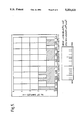
- FIG. 1 shows in cross-section a preferred ohmic contact construction within a typical device structure requiring such an ohmic contact.
- FIG. 2 is a schematic representation of thermal evaporation apparatus used to deposit the ohmic contact metals.
- FIG. 3 is a graph of a typical temperature profile of heating and cooling a graphite strip heater.
- FIG. 4 is a histogram of a typical spread of contact resistance values for an ohmic contact of the construction shown in FIG. 1.
- FIG. 5 is a histogram of a typical spread of specific contact resistivity values on the same ohmic contact as that measured for FIG. 4.
- the ohmic contact comprises a first palladium (Pd) layer 2 of 5 nm depth, a zinc (Zn) layer 3 of 10 nm depth; a second Pd layer 4 of 100 nm depth and a gold (Au) layer 5 of 400 nm depth.
- Device wafer 6 is made up of an n-type GaAs layer 7, an n-type GaAlAs layer 8, a thin p-type GaAs layer 9, an n-type GaAs layer 10 and a semiconducting n-type GaAs substrate 11. This type of layer structure would be suitable for devices. It can be seen that removal of part of layers 7 and 8 (e.g. by etching) provides access for location of ohmic contact 1 in the thin p-type GaAs layer 9.
- the ohmic contact layers were all deposited by thermal evaporation.
- ohmic contact pattern definition Prior to ohmic contact pattern definition, all exposed areas of the device layer structure are cleaned with a solvent spray for 60 seconds, suitable cleaning solvents being acetone or isopropyl alcohol. After cleaning, the definition of areas onto which the ohmic contacts are to be deposited, i.e. within accessed regions to layer 8, is carried out. This definition is often carried by a process such as lithography.
- the first step in the ohmic contact process is the deoxidation of exposed surfaces of device wafer 6. This may be carried out in a bath of 10% NH 4 in deionised water for approximately 30 seconds.
- the device wafer is then dried, most conveniently by blowing nitrogen gas over the substrate, and transferred onto a jig.
- the jig is placed in a thermal evaporator such as that which may be seen schematically in FIG. 2. The drying and transfer of the device wafer into the evaporator is carried out as quickly as possible in order to minimise the reoxidation of the exposed surfaces in the free environment.
- FIG. 2 is a schematic representation of a thermal evaporator 20 which may be used to deposit palladium, zinc and gold layers on the device wafer 6.
- Jig 21 which is carrying the device wafer, is placed in a holder 22.
- the evaporator is pumped down by pump 23 to a vacuum of 10 -6 Torr or better.
- Slugs of palladium 24, zinc 25 and gold 26 are each held in vitreous graphite crucibles 27 which are an integral Part of carousel 28. Heating of the crucibles is provided from an external power source 29 by electrical 30 to resistive heaters within the crucibles.
- the carousel is rotated to position the palladium bearing crucible approximately below the device wafer 6.
- the carousel is raised to bring the crucible nearer to the device wafer, and then the crucible is heated sufficiently to make the palladium slugs 24 become molten.
- Monitoring of the deposition rate and thickness of deposited material is carried out by the use of crystal monitor 31.
- the device wafer 6 is protected from the evaporated material by shutter 32. When the deposition rate is sufficiently high (typically about 0.5 to 0.6 nm s -1 ), the shutter is rotated away to reveal the patterned surface to the evaporated material.
- the thickness of the deposited material is monitored by the crystal monitor, with the shutter rotated back to shield the device wafer 6 when 5 nm of palladium has been deposited.
- the heating of the palladium crucible is then stopped and the carousel lowered to rotate the zinc bearing crucible under the device wafer.
- the evaporation process is then repeated to deposit about 10 nm of zinc at about 0.4 to 0.5 nm s -1 .
- the same steps are also followed for evaporation of a 100 nm palladium layer and a 400 nm gold layer, both at a rate of about 1 nm s -1 .
- the required ohmic behaviour and low contact-device material resistance is achieved by annealing to alloy the deposited metals into the p-type GaAs.
- Annealing may take place by graphite strip heater, typically for annealing temperatures of between about 250° C. and about 390° C.
- a typical annealing profile for a 360° C. anneal can be seen in FIG. 3.
- the temperature is measured by probing thermocouple on the upper surface of the device substrate 6.
- the device wafer is heated at a rate of 60° C./minute to a temperature of 50° C., point 41. It is held at this temperature for 1 minute and then heated, point 42, at a rate of 600° C./minute until a temperature of 340° C. is reached, point 43.
- the device wafer 6 is then heated to 360° C., Point 44, at a rate of 60° C./minute.
- Point 43 is usually about 20° C. below the peak annealing temperature of Point 44 in order that the slower rate of heating can then be applied and greater control of the device wafer temperature be maintained.
- annealing temperatures are between about 150° C. to about 250° C.
- Annealing times vary according to the annealing temperature used, with typical annealing times greater than about 5 minutes.
- the preferred annealing conditions are a 15 minute anneal on a 200° C. hotplate.
- Contact quality is assessed on contacts with variable transmission gap structures which are fabricated on the device wafer. By using a computer controlled autoprobing facility all such structures across a device wafer may be measured for both contact resistance and specific contact resistivity.
- FIG. 4 is a histogram showing typical distribution of contact resistance ( ⁇ -mm) of ohmic contacts of the preferred layer structure on p-type GaAs material of 5 ⁇ 10 18 cm -3 doping level.
- the contacts were manufactured using the processing steps described above.
- the mean contact resistance is 0.05041 ⁇ -mm with a standard deviation of 0.0127 ⁇ -mm.
- the ohmic contracts had undergone annealing for 15 minutes on a hotplate at a temperature of 200° C.
- FIG. 5 is a histogram showing typical distribution of specific contact resistivity ( ⁇ .cm 2 ) of ohmic contacts of the preferred layer structure on typical p-type GaAs material.
- the contacts were manufactured using the processing steps described above followed by annealing for 15 minutes on a hotplate at a temperature of 200° C.
- the mean specific contact resistivity is 0.09489 ⁇ 10 -6 ⁇ cm 2 with a standard deviation of 0.05037 ⁇ 10 -6 ⁇ cm 2
Abstract
A low resistance contact for p-type GaAs is provided by Pd/Zn/Pd/Au structure 1. The contact is suitable for device substrates having carrier concentrations in the range of about 1018 to about 1020 cm-3. The ohmic contact has a Pd layer of depth 3 nm to 15 nm, a Zn layer with a depth of between 5 nm and 40 nm, a second Pd layer with a depth greater than about 50 nm and an Au layer with a depth greater than about 300 nm. A preferred construction (1) is 5 nm/10 nm/100 nm/400 nm of Pd/Zn/Pd/Au. The ohmic contact deposition must be followed by annealing, with preferred annealing carried out at a temperature of about 200° C. Annealing times are dependent upon annealing temperature, with a typical minimum annealing times of greater than 5 minutes at annealing temperatures of about 200° C.
Description
1. Field of the Invention
This invention relates to ohmic contacts for p-type GaAs devices.
2. Discussion of the Prior Art
GaAs is a preferred material for manufacture of high speed devices such as bipolar transistors, heterojunction bipolar transistors, and p-i-n diodes. P-type GaAs and GaAlAs are often used as thin layers in multilayer devices. This means that in addition to requiring low contact resistance, in order to maximise efficient use of the higher operating speeds possible for devices made of such materials, it is also preferable to keep contact alloying heat treatment temperatures low so that inter-layer and intra-layer diffusion is minimised.
R C Brooks et al (IEEE Elect. Dev. Lett. Vol. EDL-6(10) p525 1985) detail typical specific contact resistance values of ohmic contacts for p-type GaAs using a Zn/Pd/Au metallisation. However, although specific contact resistances as low as 7×10⁻⁷ Ω.cm2 were achieved in material with 2×1019 cm-3 doping, the heat treatment temperatures needed for these values were in the range of about 420° C.-490° C.
In 1989 Yicheng Lu et al (J. Electrochem. Soc., Vol. 136, (10), p3123, 1989) used p-type GaAs (3×1017 cm-3) and Au/Zn/Au contacts to achieve specific contact resistivity of 3.3×10⁻⁶ Ω.cm2. This value does not at first appear to be as good as that given by Brooks et al (Supra). However, it must be noted that these contacts are made on much lower doped material. As a general rule, the higher the material doping then the lower the value of contact resistance. Also, the specific contact resistivity of 3.3×10⁻⁶ Ω.cm2 is corrected for sheet resistance, whereas no correction was given by Brooks et al. With no correction, then the specific contact resistance is better than the values obtained by Brooks et al.
In order to achieve the optimum contact resistivity Yicheng Lu used a two stage heat treatment process of preheating at 350° C. for 15 seconds followed by a rapid thermal anneal at 450° C. for 5 seconds.
Alternatively, C Dubon-Chevalier et al (J. Appl. Phys. 59(11), p3783, 1986) used AuMn as ohmic contacts. In the doping range of 1018 to 1019 cm-3 the specific contact resistivities varied between 10-5 and 2×10⁻⁷ Ω.cm2 respectively. The contacts had all undergone contact alloying heat treatments at 450° C.
Most recently R Bruce et al. (J of Electr Mats 19 (3) p225 1990) reported a low resistance Pd/Zn/Pd/Au ohmic contact for p-type GaAs. The contacts were formed by the sequential electron-beam evaporation of 10 nm Pd, <5 nm Zn, 20 nm Pd and 40 nm Au layers on GaAs with a doping level of 5×1018 cm-3. Minimum contact resistance of 0.04 Ω.mm (contact resistivity of <1×10⁻⁷ Ω.cm2) was obtained from such Pd/Zn/Pd/Au contacts which had been annealed at 500° C. for 30 seconds.
It is the object of this invention to provide a low contact resistance ohmic contact for p-type GaAs which may be made using low contact alloying heat treatment temperatures.
According to this invention an ohmic contact for p-type GaAs comprises:
a Pd/Zn/Pd/Au ohmic contact
characterised in that
the ohmic contact has a construction of a first layer of Pd with a depth of between 3 nm and 15 nm, a Zn layer with a depth of between 5 nm and 40 nm, a second Pd layer with a depth of greater than about 50 nm and a Au layer with a depth of greater than about 300 nm.
Preferably the second palladium (Pd) layer has a depth of between about 50 nm and about 200 nm. It is thought that the second Pd layer provides a gold (Au) diffusion barrier.
The Au layer is thought to provide a ceiling layer, and thus is not expected to have any maximum depth. Such a ceiling layer has a minimum depth of about 300 nm. Practical maximum depths of the Au layer are normally dictated by constraints of material cost and production cost, with a maximum Au layer depth of 600 nm being a typical expected maximum.
The preferred layer construction has a first palladium (Pd) layer depth of between about 5 nm and about 10 nm and a zinc (Zn) layer depth of about 10 nm. The most preferred layer construction is 5 nm/10 nm/100 nm/400 nm of Pd/Zn/Pd/Au.
Typical carrier concentrations of GaAs suitable for a Pd/Zn/Pd/Au ohmic contact are in the range of about 1018 to 1020 cm-3.
Following deposition of the contact metals it is necessary to anneal the contact. This process is used to alloy the deposited metals into the GaAs in order to achieve the required ohmic behaviour and a low contact/GaAs contact resistance. Typical annealing temperatures are between about 150° C. and about 390° C. The preferred annealing temperature is about 200° C.
Typical annealing methods include graphite strip heaters and hotplates. Preferably graphite strip heaters are used for annealing temperatures greater than about 250° C. Where graphite strip heaters are used, then the GaAs and ohmic contact are heated up to about the required annealing temperature and then cooling takes place immediately, i.e. a zero anneal hold time. At annealing temperatures below 250° C. the preferred annealing method is that of placing the contact bearing material (e.g. a substrate bearing many devices) on a pre-heated hotplate. Typically, the minimum length of time of annealing on a pre-heated hotplate is 5 minutes, dependent upon the hotplate temperature. The preferred annealing program is that of heating the hotplate to 200° C. and annealing for 15 minutes.
Suitable method of producing the ohmic contacts include thermal evaporation, electron beam evaporation and sputter coating.
The purity of the contact metals prior to use is typically about 99.999%.
The preferred deposition rates are about 0.5 to 0.6 nm s-1 for the first Pd layer, about 0.4 to 0.5 nm s-1 for the Zn layer, and about 1 nm s-1 for each of the second Pd layer and the gold (Au) layer.
The invention will now be further described by example only with reference to the following figures:
FIG. 1 shows in cross-section a preferred ohmic contact construction within a typical device structure requiring such an ohmic contact.
FIG. 2 is a schematic representation of thermal evaporation apparatus used to deposit the ohmic contact metals.
FIG. 3 is a graph of a typical temperature profile of heating and cooling a graphite strip heater.
FIG. 4 is a histogram of a typical spread of contact resistance values for an ohmic contact of the construction shown in FIG. 1.
FIG. 5 is a histogram of a typical spread of specific contact resistivity values on the same ohmic contact as that measured for FIG. 4.
A cross-section of the preferred construction of ohmic contact 1 can be seen in FIG. 1. The ohmic contact comprises a first palladium (Pd) layer 2 of 5 nm depth, a zinc (Zn) layer 3 of 10 nm depth; a second Pd layer 4 of 100 nm depth and a gold (Au) layer 5 of 400 nm depth. Device wafer 6 is made up of an n-type GaAs layer 7, an n-type GaAlAs layer 8, a thin p-type GaAs layer 9, an n-type GaAs layer 10 and a semiconducting n-type GaAs substrate 11. This type of layer structure would be suitable for devices. It can be seen that removal of part of layers 7 and 8 (e.g. by etching) provides access for location of ohmic contact 1 in the thin p-type GaAs layer 9. The ohmic contact layers were all deposited by thermal evaporation.
Prior to ohmic contact pattern definition, all exposed areas of the device layer structure are cleaned with a solvent spray for 60 seconds, suitable cleaning solvents being acetone or isopropyl alcohol. After cleaning, the definition of areas onto which the ohmic contacts are to be deposited, i.e. within accessed regions to layer 8, is carried out. This definition is often carried by a process such as lithography.
The first step in the ohmic contact process is the deoxidation of exposed surfaces of device wafer 6. This may be carried out in a bath of 10% NH4 in deionised water for approximately 30 seconds. The device wafer is then dried, most conveniently by blowing nitrogen gas over the substrate, and transferred onto a jig. The jig is placed in a thermal evaporator such as that which may be seen schematically in FIG. 2. The drying and transfer of the device wafer into the evaporator is carried out as quickly as possible in order to minimise the reoxidation of the exposed surfaces in the free environment.
FIG. 2 is a schematic representation of a thermal evaporator 20 which may be used to deposit palladium, zinc and gold layers on the device wafer 6. Jig 21, which is carrying the device wafer, is placed in a holder 22. The evaporator is pumped down by pump 23 to a vacuum of 10-6 Torr or better. Slugs of palladium 24, zinc 25 and gold 26 are each held in vitreous graphite crucibles 27 which are an integral Part of carousel 28. Heating of the crucibles is provided from an external power source 29 by electrical 30 to resistive heaters within the crucibles.
The carousel is rotated to position the palladium bearing crucible approximately below the device wafer 6. The carousel is raised to bring the crucible nearer to the device wafer, and then the crucible is heated sufficiently to make the palladium slugs 24 become molten. Monitoring of the deposition rate and thickness of deposited material is carried out by the use of crystal monitor 31. The device wafer 6 is protected from the evaporated material by shutter 32. When the deposition rate is sufficiently high (typically about 0.5 to 0.6 nm s-1), the shutter is rotated away to reveal the patterned surface to the evaporated material. The thickness of the deposited material is monitored by the crystal monitor, with the shutter rotated back to shield the device wafer 6 when 5 nm of palladium has been deposited. The heating of the palladium crucible is then stopped and the carousel lowered to rotate the zinc bearing crucible under the device wafer. The evaporation process is then repeated to deposit about 10 nm of zinc at about 0.4 to 0.5 nm s-1. The same steps are also followed for evaporation of a 100 nm palladium layer and a 400 nm gold layer, both at a rate of about 1 nm s-1.
Following deposition of the Pd/Zn/Pd/Au to form an ohmic contact, the required ohmic behaviour and low contact-device material resistance is achieved by annealing to alloy the deposited metals into the p-type GaAs. Annealing may take place by graphite strip heater, typically for annealing temperatures of between about 250° C. and about 390° C. A typical annealing profile for a 360° C. anneal can be seen in FIG. 3.
The temperature is measured by probing thermocouple on the upper surface of the device substrate 6. At room temperature, point 40, the device wafer is heated at a rate of 60° C./minute to a temperature of 50° C., point 41. It is held at this temperature for 1 minute and then heated, point 42, at a rate of 600° C./minute until a temperature of 340° C. is reached, point 43. The device wafer 6 is then heated to 360° C., Point 44, at a rate of 60° C./minute. The heating is then turned off and natural cooling occurs. Point 43 is usually about 20° C. below the peak annealing temperature of Point 44 in order that the slower rate of heating can then be applied and greater control of the device wafer temperature be maintained.
However, it has been found that superior contact resistances and specific contact resistivities have been achieved by use of lower annealing temperatures. The device wafer 6 is taken out of the jig 21 and placed, with the device surface uppermost, on a pre-heated hotplate. Typical hotplate temperatures are between about 150° C. to about 250° C. Annealing times vary according to the annealing temperature used, with typical annealing times greater than about 5 minutes. The preferred annealing conditions are a 15 minute anneal on a 200° C. hotplate.
Contact quality is assessed on contacts with variable transmission gap structures which are fabricated on the device wafer. By using a computer controlled autoprobing facility all such structures across a device wafer may be measured for both contact resistance and specific contact resistivity.
FIG. 4 is a histogram showing typical distribution of contact resistance (Ω-mm) of ohmic contacts of the preferred layer structure on p-type GaAs material of 5×1018 cm-3 doping level. The contacts were manufactured using the processing steps described above. The mean contact resistance is 0.05041 Ω-mm with a standard deviation of 0.0127 Ω-mm. The ohmic contracts had undergone annealing for 15 minutes on a hotplate at a temperature of 200° C.
FIG. 5 is a histogram showing typical distribution of specific contact resistivity (Ω.cm2) of ohmic contacts of the preferred layer structure on typical p-type GaAs material. The contacts were manufactured using the processing steps described above followed by annealing for 15 minutes on a hotplate at a temperature of 200° C. The mean specific contact resistivity is 0.09489×10⁻⁶ Ωcm2 with a standard deviation of 0.05037×10⁻⁶ Ωcm2
Claims (11)
1. An ohmic contact for p-type GaAs comprising:
a Pd/Zn/Pd/Au ohmic contact
characterised in that
the ohmic contact has a construction of a first layer of Pd with a depth of between 3 nm and 15 nm, a Zn layer with a depth of between 5 nm and 40 nm, a second Pd layer with a depth of greater than about 50 nm and a Au layer with a depth of greater than about 300 nm.
2. An ohmic contact as claimed in claim 1 where the first palladium layer has a depth of between about 5 nm and about 10 nm.
3. An ohmic contact as claimed in claim 1 where the first palladium layer has a depth of about 5 nm.
4. An ohmic contact as claimed in claim 1 where the zinc layer has a depth of about 10 nm.
5. An ohmic contact as claimed in claim 1 where the second palladium layer has a depth of about 100 nm.
6. An ohmic contact as claimed in claim 1 where the gold layer has a depth of about 400 nm.
7. An ohmic contact as claimed in claim 1 where the multiple layer structure has respective depths of 5 nm/10 nm/100 nm/400 nm.
8. An ohmic contact as claimed in claim 1 annealed at a temperature of between about 150° C. and about 390° C.
9. An ohmic contact as claimed in claim 8 annealed at 200° C.
10. An ohmic contact as claimed in claim 8 annealed for a minimum of 5 minutes.
11. An ohmic contact as claimed in claim 9 annealed for 15 minutes.
Applications Claiming Priority (3)
| Application Number | Priority Date | Filing Date | Title |
|---|---|---|---|
| GB9015871 | 1990-07-19 | ||
| GB909015871A GB9015871D0 (en) | 1990-07-19 | 1990-07-19 | Ohmic contact for p-type gaas |
| PCT/GB1991/001198 WO1992002037A1 (en) | 1990-07-19 | 1991-07-18 | OHMIC CONTACT FOR P-TYPE GaAs |
Publications (1)
| Publication Number | Publication Date |
|---|---|
| US5355021A true US5355021A (en) | 1994-10-11 |
Family
ID=10679331
Family Applications (1)
| Application Number | Title | Priority Date | Filing Date |
|---|---|---|---|
| US08/075,460 Expired - Fee Related US5355021A (en) | 1990-07-19 | 1991-07-18 | Ohmic contact for p-type GaAs |
Country Status (4)
| Country | Link |
|---|---|
| US (1) | US5355021A (en) |
| EP (1) | EP0552159A1 (en) |
| GB (1) | GB9015871D0 (en) |
| WO (1) | WO1992002037A1 (en) |
Cited By (7)
| Publication number | Priority date | Publication date | Assignee | Title |
|---|---|---|---|---|
| US5840612A (en) * | 1996-05-13 | 1998-11-24 | Trw Inc. | Method of fabricating very high gain heterojunction bipolar transistors |
| US6188137B1 (en) * | 1995-05-25 | 2001-02-13 | Sharp Kabushiki Kaisha | Ohmic electrode structure, semiconductor device including such ohmic electrode structure, and method for producing such semiconductor device |
| US10833199B2 (en) | 2016-11-18 | 2020-11-10 | Acorn Semi, Llc | Nanowire transistor with source and drain induced by electrical contacts with negative Schottky barrier height |
| US10872964B2 (en) | 2016-06-17 | 2020-12-22 | Acorn Semi, Llc | MIS contact structure with metal oxide conductor |
| US10879366B2 (en) | 2011-11-23 | 2020-12-29 | Acorn Semi, Llc | Metal contacts to group IV semiconductors by inserting interfacial atomic monolayers |
| US10937880B2 (en) | 2002-08-12 | 2021-03-02 | Acorn Semi, Llc | Method for depinning the Fermi level of a semiconductor at an electrical junction and devices incorporating such junctions |
| US11043571B2 (en) | 2002-08-12 | 2021-06-22 | Acorn Semi, Llc | Insulated gate field effect transistor having passivated schottky barriers to the channel |
Families Citing this family (1)
| Publication number | Priority date | Publication date | Assignee | Title |
|---|---|---|---|---|
| US7341882B2 (en) * | 2003-11-18 | 2008-03-11 | Uni Light Technology Inc. | Method for forming an opto-electronic device |
Citations (1)
| Publication number | Priority date | Publication date | Assignee | Title |
|---|---|---|---|---|
| US4395727A (en) * | 1980-03-27 | 1983-07-26 | Siemens Aktiengesellschaft | Barrier-free, low-resistant electrical contact on III-V semiconductor material |
-
1990
- 1990-07-19 GB GB909015871A patent/GB9015871D0/en active Pending
-
1991
- 1991-07-18 US US08/075,460 patent/US5355021A/en not_active Expired - Fee Related
- 1991-07-18 WO PCT/GB1991/001198 patent/WO1992002037A1/en not_active Application Discontinuation
- 1991-07-18 EP EP91913565A patent/EP0552159A1/en not_active Withdrawn
Patent Citations (1)
| Publication number | Priority date | Publication date | Assignee | Title |
|---|---|---|---|---|
| US4395727A (en) * | 1980-03-27 | 1983-07-26 | Siemens Aktiengesellschaft | Barrier-free, low-resistant electrical contact on III-V semiconductor material |
Non-Patent Citations (8)
| Title |
|---|
| Journal of Applied Physics, vol. 59, No. 10, May 1986, Kobayashi et al "An Atomistic Study Of The GaAs-Pd Interface"pp. 3448-3453. |
| Journal of Applied Physics, vol. 59, No. 10, May 1986, Kobayashi et al An Atomistic Study Of The GaAs Pd Interface pp. 3448 3453. * |
| Journal of Electronic Materials, vol. 19, No. 3, 1990, Bruce et al, "Low Resistant Pd/Zn/PdAu Ohmic Contacts of P-Type GaAs", pp. 225-229. |
| Journal of Electronic Materials, vol. 19, No. 3, 1990, Bruce et al, Low Resistant Pd/Zn/PdAu Ohmic Contacts of P Type GaAs , pp. 225 229. * |
| Journal of Electronic Materials, vol. 20, No. 3, 1991, Ivey et al "Pd/Zn/Pd/Au Ohmic Contacts to P-Type GaAs" pp. 237-246. |
| Journal of Electronic Materials, vol. 20, No. 3, 1991, Ivey et al Pd/Zn/Pd/Au Ohmic Contacts to P Type GaAs pp. 237 246. * |
| Materials Letters, vol. 8, No. 10, Oct. 1989, Ivey et al: "Expitaxially Grown PdzInP on InP" pp. 389-395. |
| Materials Letters, vol. 8, No. 10, Oct. 1989, Ivey et al: Expitaxially Grown PdzInP on InP pp. 389 395. * |
Cited By (15)
| Publication number | Priority date | Publication date | Assignee | Title |
|---|---|---|---|---|
| US6188137B1 (en) * | 1995-05-25 | 2001-02-13 | Sharp Kabushiki Kaisha | Ohmic electrode structure, semiconductor device including such ohmic electrode structure, and method for producing such semiconductor device |
| US5840612A (en) * | 1996-05-13 | 1998-11-24 | Trw Inc. | Method of fabricating very high gain heterojunction bipolar transistors |
| US11056569B2 (en) | 2002-08-12 | 2021-07-06 | Acorn Semi, Llc | Method for depinning the fermi level of a semiconductor at an electrical junction and devices incorporating such junctions |
| US10937880B2 (en) | 2002-08-12 | 2021-03-02 | Acorn Semi, Llc | Method for depinning the Fermi level of a semiconductor at an electrical junction and devices incorporating such junctions |
| US10950707B2 (en) | 2002-08-12 | 2021-03-16 | Acorn Semi, Llc | Method for depinning the Fermi level of a semiconductor at an electrical junction and devices incorporating such junctions |
| US11018237B2 (en) | 2002-08-12 | 2021-05-25 | Acorn Semi, Llc | Method for depinning the fermi level of a semiconductor at an electrical junction and devices incorporating such junctions |
| US11043571B2 (en) | 2002-08-12 | 2021-06-22 | Acorn Semi, Llc | Insulated gate field effect transistor having passivated schottky barriers to the channel |
| US11355613B2 (en) | 2002-08-12 | 2022-06-07 | Acorn Semi, Llc | Method for depinning the Fermi level of a semiconductor at an electrical junction and devices incorporating such junctions |
| US10879366B2 (en) | 2011-11-23 | 2020-12-29 | Acorn Semi, Llc | Metal contacts to group IV semiconductors by inserting interfacial atomic monolayers |
| US11610974B2 (en) | 2011-11-23 | 2023-03-21 | Acorn Semi, Llc | Metal contacts to group IV semiconductors by inserting interfacial atomic monolayers |
| US11804533B2 (en) | 2011-11-23 | 2023-10-31 | Acorn Semi, Llc | Metal contacts to group IV semiconductors by inserting interfacial atomic monolayers |
| US10872964B2 (en) | 2016-06-17 | 2020-12-22 | Acorn Semi, Llc | MIS contact structure with metal oxide conductor |
| US11843040B2 (en) | 2016-06-17 | 2023-12-12 | Acorn Semi, Llc | MIS contact structure with metal oxide conductor |
| US10833199B2 (en) | 2016-11-18 | 2020-11-10 | Acorn Semi, Llc | Nanowire transistor with source and drain induced by electrical contacts with negative Schottky barrier height |
| US11462643B2 (en) | 2016-11-18 | 2022-10-04 | Acorn Semi, Llc | Nanowire transistor with source and drain induced by electrical contacts with negative Schottky barrier height |
Also Published As
| Publication number | Publication date |
|---|---|
| EP0552159A1 (en) | 1993-07-28 |
| GB9015871D0 (en) | 1990-09-05 |
| WO1992002037A1 (en) | 1992-02-06 |
Similar Documents
| Publication | Publication Date | Title |
|---|---|---|
| Chu et al. | Degenerate cadmium oxide films for electronic devices | |
| US5406123A (en) | Single crystal titanium nitride epitaxial on silicon | |
| Fonash et al. | Effect of ion‐beam sputter damage on Schottky barrier formation in silicon | |
| US6117771A (en) | Method for depositing cobalt | |
| KR100279106B1 (en) | Manufacturing method of semiconductor device | |
| KR100543717B1 (en) | Method for Annealing Silicon Thin Films and Polycrystalline Silicon Thin Films Prepared Therefrom | |
| JPH1187242A (en) | Amorphous film crystallizing method and thin-film transistor | |
| US4545115A (en) | Method and apparatus for making ohmic and/or Schottky barrier contacts to semiconductor substrates | |
| KR20030060403A (en) | crystallization method of amorphous silicon | |
| US4468308A (en) | Metallic silicide production | |
| US5355021A (en) | Ohmic contact for p-type GaAs | |
| US4522845A (en) | Process for producing a layer of a metal silicide by applying multichromatic radiation | |
| US5309022A (en) | Ni-Ge-Au ohmic contacts for GaAs and GaAlAs | |
| Aina et al. | Low‐temperature sintered AuGe/GaAs ohmic contact | |
| KR0161376B1 (en) | Method for forming metal interconnection and sputtering apparatus for this method | |
| Krutko et al. | P-type polycrystalline diamond layers by rapid thermal diffusion of boron | |
| JPS6139731B2 (en) | ||
| Simeonov et al. | Preparation of Mo/Si Schottky barriers by chemical vapour deposition of molybdenum onto epitaxial silicon substrates | |
| US4519850A (en) | Process for the thermo-migration of liquid phases | |
| JP2001135591A (en) | Method of manufacturing semiconductor element | |
| Kwong | Rapid thermal annealing of co-sputtered tantalum silicide films | |
| Vaidya | Electromigration in aluminum/poly‐silicon composites | |
| US11195732B2 (en) | Low thermal budget annealing | |
| JPH088205A (en) | Manufacture of semiconductor element | |
| JPS61185923A (en) | Formation of semiconductor low resistance layer |
Legal Events
| Date | Code | Title | Description |
|---|---|---|---|
| AS | Assignment |
Owner name: SECRETARY OF STATE FOR DEFENCE IN HER BRITANNIC MA Free format text: ASSIGNMENT OF ASSIGNORS INTEREST;ASSIGNORS:CROUCH, MARK ANTHONY;GILL, SUHKDEV SINGH;GILBEY, WILLIAM HUGH;AND OTHERS;REEL/FRAME:006788/0530 Effective date: 19930526 |
|
| REMI | Maintenance fee reminder mailed | ||
| LAPS | Lapse for failure to pay maintenance fees | ||
| FP | Lapsed due to failure to pay maintenance fee |
Effective date: 19981011 |
|
| STCH | Information on status: patent discontinuation |
Free format text: PATENT EXPIRED DUE TO NONPAYMENT OF MAINTENANCE FEES UNDER 37 CFR 1.362 |