US5329179A - Arrangement for parallel programming of in-system programmable IC logical devices - Google Patents
Arrangement for parallel programming of in-system programmable IC logical devices Download PDFInfo
- Publication number
- US5329179A US5329179A US07/957,311 US95731192A US5329179A US 5329179 A US5329179 A US 5329179A US 95731192 A US95731192 A US 95731192A US 5329179 A US5329179 A US 5329179A
- Authority
- US
- United States
- Prior art keywords
- programming
- command generator
- devices
- isp
- logic devices
- Prior art date
- Legal status (The legal status is an assumption and is not a legal conclusion. Google has not performed a legal analysis and makes no representation as to the accuracy of the status listed.)
- Expired - Fee Related
Links
Images


Classifications
-
- G—PHYSICS
- G06—COMPUTING; CALCULATING OR COUNTING
- G06F—ELECTRIC DIGITAL DATA PROCESSING
- G06F30/00—Computer-aided design [CAD]
- G06F30/30—Circuit design
- G06F30/34—Circuit design for reconfigurable circuits, e.g. field programmable gate arrays [FPGA] or programmable logic devices [PLD]
Definitions
- This invention relates to in-system programmable IC logic devices and, in particular, to a parallel arrangement for programming such devices.
- ISP In-system programmable
- U.S. Pat. No. 4,870,302 illustrates (FIGS. 8A and 8B) two systems for programming a group of ISP devices.
- the ISP are connected in series, so that the programming data must be transferred through each device in the series before arriving at the intended destination device.
- U.S. application Ser. No. 07/695,356 commonly owned and incorporated by reference herein, describes an arrangement for programming a group of ISP devices that are connected in series.
- a programming command generator is connected in parallel with a group of ISP logic devices.
- a device selector is used to connect the programming command generator to a desired ISP device, thereby allowing the programming data to be delivered directly to that device without passing through intermediate devices.
- Several configurations for the device selector are described, including a demultiplexer, a state machine-controlled demultiplexer, a switch matrix, and a state machine-controlled switch matrix. These possibilities are not exhaustive, however; other equivalent arrangements will be apparent to those skilled in the art and are included within the broad principles of this invention.
- an advantage of this arrangement is that the programming data may first be read into each of the devices separately, and then all of the devices can be programmed simultaneously. This substantially reduces the amount of time required to program the devices.
- the device selector is omitted and the device to be programmed is selected by transmitting an identification code unique to that device so as to establish communication between that device alone and the programming command generator.
- FIG. 1 illustrates a block diagram of an embodiment of the invention which includes a demultiplexer.
- FIG. 2 illustrates a flow chart of the state machine in the ISP devices.
- FIG. 3 illustrates the general structure of an ISP device having four input signals.
- FIG. 4 illustrates the general structure of an ISP device having five input signals.
- FIG. 5 illustrates a block diagram of an embodiment of the invention which includes a state machine-controlled demultiplexer.
- FIG. 6 illustrates a flow chart of the state machine in the state machine-controlled multiplexer of FIG. 5.
- FIG. 7 illustrates a block diagram of an embodiment of the invention which includes a switch matrix.
- FIG. 8 illustrates a block diagram of an embodiment of the invention which includes a state machine-controlled switch matrix.
- FIGS. 9, 9A and 9B illustrate a block diagram of an embodiment of the invention which does not include a device selector.
- the first of these devices is the ispGAL22V10, which has four programming pins: Mode, SCLK (Serial Clock), SDI (Serial Data In), and SDO (Serial Data Out).
- Mode SCLK (Serial Clock)
- SDI Serial Data In
- SDO Serial Data Out
- the device is placed in the programming mode by asserting the Mode signal high. Thereafter, the programming operation is controlled by the Mode and SDI pins.
- the structure and operation of this device are outlined below and are fully described in the ispGAL22V10 Programmer's Guide, available from Lattice Semiconductor Corporation, which is incorporated herein by reference.
- the second device is the Lattice ispLSI.
- This device is programmed by using five pins, designated: ispEN(isp Enable), Mode, SCLK, SCI and SCO.
- This device is placed in the programming mode by asserting the ispENpin low, which converts the other four pins from their normal functions to the programming mode. Thereafter, the programming is controlled by the Mode and SDI pins.
- the structure and operation of this device are outlined below and are fully described in the ispLSI Family Programming Spec., also available from Lattice Semiconductor Corporation and incorporated herein by reference.
- ISP devices 1, 2 and 3 are ispGAL22V10s and are therefore programmed using four pins
- ISP devices 4, 5 and 6 are ispLSIs and therefore are programmed using five pins.
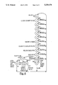
- FIG. 1 illustrates an embodiment in which the device selector is a demultiplexer.
- a programming command generator 10 provides all of the signals necessary to program ISP devices 1-6 on lines designated Mode, SCLK, SDI, SDO and ispEN.
- Programming command generator 10 may, for example, be an IBM PC.
- a program suitable for programming command generator 10 is set forth at pp. 4-33 to 4-39 of the Lattice pLSI and ispLSI Data Book and Handbook (1992), available from Lattice Semiconductor Corp., which is incorporated herein by reference in its entirety.
- Programming command generator 10 is connected to a demultiplexer 11 via a latch 12, which holds a 3-bit word designating which of ISP devices 1-6 is to be addressed.
- Demultiplexer 11 contains a decoder 13 having six outputs which control respective switches 14A-14F.
- the Mode output of programming command generator 10 connects to one side of switches 14A-14C which in turn run to ISP devices 1-3.
- the ispENoutput of programming command generator 10 is connected to one side of switches 14D-14F which in turn run to devices 4-6.
- programming command generator 10 outputs a 001 to latch 12, and decoder 13 generates an output closing switch 14A, which connects the Mode line to ISP device 1.
- switch 14A is opened.
- programming command generator 10 outputs a 100 to latch 12, and decoder 13 generates an output closing switch 14D, which connects the ispENline to ISP device 4.
- switch 14D is opened.
- Program command generator cannot communicate with those of ISP devices 1-6 which correspond to any of switches 14A-14F that are open, and thus they do not recognize the programming command.
- FIG. 3 illustrates a block diagram of the internal interface to the ISP pins and the functional units involved in the programming operation.
- the programming operation is controlled by an instruction-based state machine 200 which is illustrated in FIG. 2.
- State machine 200 includes three states 201, 202 and 203, corresponding respectively to the idle, shift and execute states. Timing of state machine 200 is provided by the clock signal on the SCLK pin.
- the state of state machine 200 is determined by the signals on the Mode and SDI pins, and every state change is effective at the next clock pulse after a change in the Mode and SDI inputs.
- state machine 200 stays locked in the idle state 201, which is unlocked when a high logic signal is received at the mode pin.
- idle state 201 can be entered at any time from any state after one clock pulse by bringing the signal on the Mode pin to a logic high and the signal on the SDI pin to a logic low.
- a transition from the idle state 201 to the shift state 202, from the shift state to the execute state 203, or from the execute state 203 back to the shift state 202 can be accomplished by bringing both the Mode and the SDI pins to a logic high.
- the Mode pin is at a logic low, the SDI pin is a data input pin, and the current state is held.
- an 8-bit identification is automatically loaded into an ID register 301.
- the 8-bit identification specifies such parametric values as the number of logic blocks on the chip, the number of I/O pins available, etc. and is "hard wired" into the device.
- the Mode pin goes to a logic low, and seven clock pulses are applied to the SCLK pin to shift the identification in ID register 301 out the SDO pin to programming command generator 10 (the least significant bit of the identification already appears on the SDO pin). If programming command generator 10 recognizes the identification, communication is established with the ISP device.
- the shift state 202 is entered from the idle state 201 by bringing both the Mode and the SDI pins to a logic high.
- a 5-bit command is shifted serially into the ISP device via the SDI line.
- the command may be to erase data in the ISP device, send programming data to the ISP device, program the ISP device according to the data sent, extract programming data from the ISP device, or test the ISP device.
- Execution of the command is effected by bringing state machine 200 to the execute state 203, which is entered from the shift state 202 by bringing both the Mode and SDI pins to a logic high.
- Using 5-bit commands 32 commands can be defined. The commands for device 4 are shown in Appendix A.
- the command stored in the ISP device is executed. If the instruction is to load programming data into a data register 302 (i.e., the command "DATASHFT"), for example, the appropriate number of bits are shifted into data register 302 from the SDI pin after the Mode pin goes to a logic low, while the same number of bits in data register 302 are shifted out the SDO pin back to programming command generator 10. After the programming data have been shifted into register 302, a 5-bit command is issued to the ISP device by programming command generator 10 to transfer the programming data to row address 00 in a memory array 303.
- Array 303 contains a number of memory locations which correspond to programmable connections in the ISP device.
- ISP device 4 is illustrated in FIG. 4.
- State machine 400 is substantially identical to state machine 200 shown in FIG. 2. State machine 400 is activated when the ispENis driven low, and its transitions from one state to another are controlled by the Mode and SDI pins. Initially state machine 400 is instructed to load into an ID register 401 an 8-bit identification which is then shifted out via the SDO line to programming command generator 10.
- programming command generator 10 recognizes the identification, communication is established with ISP device 4.
- Programming command generator 10 then commands state machine 400 to shift the programming data into a data register 402 via the SDI line.
- State machine 400 is then commanded to shift row selection data into a row register 404. In FIG. 4, row 0 is selected.
- the programming data are then transferred from data register 402 to row 0 in a programmable array 403. This process is repeated until all of rows 0 through 107 are filled with programming data.
- the programmable connections in ISP device 4 are then programmed in accordance with the data stored in array 403.
- the SCLK, SDI and SDO outputs of programming command generator 10 are connected in common to ISP devices 1-3, while the Mode output is connected to ISP devices 1-3 via demultiplexer 11.
- the Mode, SCLK, SDI and SDO outputs of programming command generator 10 are connected in common to ISP devices 4-6, while the ispENoutput is connected to ISP devices 4-6 via demultiplexer 11.
- the respective state machines in ISP devices 1-3 are activated via the Mode pin
- the respective state machines in ISP devices 4-6 are activated via the ispENpin.
- a state machine-controlled demultiplexer 50 is connected between programming command generator 10 and ISP devices 1-6.
- State machine-controlled demultiplexer 50 contains a state machine 51, a counter 52, a decoder 53 and switches 54A-54F.
- the ispENoutput of programming command generator 10 is connected to an input of state machine 50 and to one side of switches 54D-54F.
- the Mode output of programming command generator 10 is connected to another input of state machine 50 and to one side of switches 54A-54C.
- the SDI output of programming command generator 50 is connected to another input of state machine 50. Clock pulses are provided to state machine 50 and counter 52 via the SCLK output of programming command generator 10.
- State machine 51 and counter 52 may advantageously reside in a Lattice GAL6001, the programming and structure of which are described in Appendix B and at pp. 2-147 to 2-161 of the Lattice GAL Data Book (1992), available from Lattice Semiconductor Corporation and incorporated herein by reference.
- the control signals for state machine 51 are Mode and SDI.
- Each GAL6001 device can support 7, ISP devices, since it includes a 3-bit counter.
- the 3-bit counters of several GAL6001 devices may be cascaded together to support as many ISP devices as required, as illustrated on page 17 of Appendix B.
- FIG. 6 illustrates a flow chart for state machine 51, which includes fourteen "states”. Movement from one state to the next is controlled by the output of the SDI and Mode lines, and occurs with the clock pulses on the SCLK line. Since the SDI line is connected in common to state machine 51 as well as ISP devices 1-6, it is important to avoid issuing instructions to state machine 51 that would prompt any unwanted actions to be taken by ISP devices 1-6. This concern is accommodated by using the "no operation" command "00000” as a “wake-up” command for state machine 51 (see Appendix A).
- State machine 51 is activated by bringing the ispENline to a logic low, which places state machine 51 in state 0.
- the SDI and Mode lines are then brought to a logic high to move state machine 51 to state 1.
- This moves state machines 200 in ISP devices 103 and state machines 400 in ISP devices 4-6 to the "shift" state 202 (see FIG. 2).
- the SDI line is brought to a logic low for five consecutive clock pulses, bringing state machine 51 to state 6.
- ISP devices 1.6 interpret this as a "no operation" command 00000 while it serves as a "wake-up" command for state machine 51.
- the SDI and Mode lines are then brought to a logic high, bringing state machine 51 to state 7 and the state machines in ISP devices 1-6 to the "execute" state 203.
- state machine 51 moves to state 8
- state machines in ISP devices 1-6 execute the command. Since the command was "no operation” however no action is taken as a result of this command.
- the SDI line is then brought high and the Mode line is brought low, moving state machine 51 to state 9, and moving the state machines in ISP devices 1-6 from the "execute” state to the "idle” state. This completes the “wake-up” cycle for state machine 51, and results in the state machines in ISP devices 1-6 being in the "idle” state.
- These state machines will remain in the "idle” state so long as a logic high does not appear on both the SDI and Mode lines.
- the SDI and Mode lines are then both brought low, which resets counter 52 to zero. If the SDI and Mode lines remain low, state machine 51 proceeds to state 11.
- the Mode line is then brought to a logic high, and remains in this condition as programming command generator 10 delivers a number of clock pulses representative of the ISP device to be selected. Each of these clock pulses causes counter 52 to advance one binary word. For example, if ISP device 5 is to be selected, five clock pulses would be delivered to counter 52 leaving it in a "101" state.
- the binary word in counter 52 is reflected at all times in decoder 53, so that switches 54A, 54B, etc. are closed in succession as counter 52 steps forward.
- the desired number is reached (i.e., the desired one of switches 54A-54F is closed)
- the SDI line is brought to a logic high and state machine 51 moves to state 12. This terminates the clocking of counter 52 and leaves the desired switch closed.
- States 13 and 14 are optional features that are not required for programming the ISP devices.
- the use of state 13 allows the user to receive a visual reading of which ISP device has been selected.
- state machine 51 arrives at state 11, the Mode line is brought low, moving state machine 51 to state 13.
- the SDI line is then brought low and the Mode line is brought high and counter 52 is pulsed as described above.
- the user is given a visual indication of which device has been selected. If the visual indication indicates that the correct device has been selected, both the SDI and Mode lines are brought high, causing the device to be enabled. Otherwise, if the Mode line is brought low, the device remains disabled.
- State 14 is used in the situation where more than seven ISP devices are being programmed. As noted above, since counter 52 is a 3-bit counter this requires that at least one additional counter be cascaded with counter 52. In this configuration, when state machine 51 reaches a "111" the next clock pulse would drive the second counter to a "001". Each time a counter fills up, a "1" appears on the line connecting it with the next cascaded counter, and in the case of the last counter on the SDO line. When state machine 51 is moved to state 14, programming command generator 10 counts the pulses delivered on the SCLK line while monitoring the SDO line. When a "1" appears on the SDO line, programming command generator 10 can determine the number of counters cascaded by dividing the number of pulses delivered by seven. This enables the user to determine how many counters are cascaded together.
- FIG. 7 shows an embodiment including switch matrixes 70 and 71.
- Latch 12 and decoder 13 are identical to the similarly numbered components shown in FIG. 1.
- Three outputs of decoder 12 control switch groups in matrix 70, which connect the Mode, SCLK, SDI and SDO outputs to ISP devices 1-3, respectively.
- the remaining three outputs of decoder 13 control switch groups in switch matrix 71, and connect the Mode, SCLK, SDI, SDO and ispENto ISP devices 4-6, respectively.
- FIG. 7 if the numeral 001 is delivered to latch 12, decoder 13 will close the switches connecting programming command generator 10 to ISP device 1.
- ISP Device 1 is then programmed as described above.
- ISP devices 2-6 may be connected to programming command generator 10 and programmed.
- FIG. 8 illustrates yet another embodiment which includes a state machine controlled switch matrix 80.
- State machine 51, counter 52 and decoder 53 are identical to the similarly numbered components shown in FIG. 5. These devices function together in the same manner described above in connection with FIG. 5 to close the desired group of switches in switch matrix 80, thereby connecting the required output lines from programming command generator 10 to a desired one of ISP devices 1-6.
- FIG. 9 illustrates another embodiment which omits the device selector.
- ISP devices 4-6 are shown connected to program command generator 10.
- Each of ISP devices 4-6 has a different 8-bit identification, the identification being "0000001" for ISP device 4, "00000010” for ISP device 5, and "00000011” for ISP device 6.
- Program command generator 10 drives the ispENlow, which results in the identification being loaded into the ID register 401 in each device.
- ISP device 4 is to be programmed.
- Programming command generator 10 shifts the identification of ISP device 4 ("00000001") into the ID register 401 in each of the devices.
- a comparison means in each device compares the identification in ID register 401 with the permanently stored identification in the device, and as a result a match occurs only in ISP device 4. Therefore, communication is established only with ISP device 4 for data transfer from programming command generator 10, and ISP devices 5 and 6 are not activated for programming.
- Programming command generator 10 then shifts the programming data into the data register 402 and the row address information into row register 404 of ISP device 4. Programming command generator 10 then drives the Mode pin high and the SDI pin low and pulses the SCLK pin. This loads the internally stored identification of each device into its respective ID register 401.
- the embodiments described above have various advantages and disadvantages.
- the system which includes a demultiplexer (FIG. 1) uses a minimal traces on a circuit board and can support any mix of ISP devices. However, it does require the addition of a demultiplexer and additional trace circuitry is required to connect programming command generator 10 with latch 12.
- the system which includes a state machine-controlled multiplexor (FIG. 5) requires minimal traces on a circuit board and can also support any mix of ISP devices. No additional traces are required to connect programming command generator 10 to state machine-controlled demultiplexer 50, and the programming time is minimized by programming all of the ISP devices simultaneously. However, this system requires a fairly complex IC for the state machine-controlled multiplexor.
- FIGS. 7 and 8 The embodiments which include a switch matrix (FIGS. 7 and 8) require a greater number of traces on a printed circuit board.
- FIG. 9 requires minimal traces on a circuit board, and no additional component such as a multiplexor is required. Moreover, programming time is minimized because all of the ISP devices can be programmed simultaneously. However, none of the ISP devices may have exactly the same identity.
Abstract
Description
Claims (6)
Priority Applications (2)
| Application Number | Priority Date | Filing Date | Title |
|---|---|---|---|
| US07/957,311 US5329179A (en) | 1992-10-05 | 1992-10-05 | Arrangement for parallel programming of in-system programmable IC logical devices |
| PCT/US1993/009289 WO1994008399A1 (en) | 1992-10-05 | 1993-10-05 | Arrangement for parallel programming of in-system programmable ic logic devices |
Applications Claiming Priority (1)
| Application Number | Priority Date | Filing Date | Title |
|---|---|---|---|
| US07/957,311 US5329179A (en) | 1992-10-05 | 1992-10-05 | Arrangement for parallel programming of in-system programmable IC logical devices |
Publications (1)
| Publication Number | Publication Date |
|---|---|
| US5329179A true US5329179A (en) | 1994-07-12 |
Family
ID=25499406
Family Applications (1)
| Application Number | Title | Priority Date | Filing Date |
|---|---|---|---|
| US07/957,311 Expired - Fee Related US5329179A (en) | 1992-10-05 | 1992-10-05 | Arrangement for parallel programming of in-system programmable IC logical devices |
Country Status (2)
| Country | Link |
|---|---|
| US (1) | US5329179A (en) |
| WO (1) | WO1994008399A1 (en) |
Cited By (11)
| Publication number | Priority date | Publication date | Assignee | Title |
|---|---|---|---|---|
| US5394031A (en) * | 1993-12-08 | 1995-02-28 | At&T Corp. | Apparatus and method to improve programming speed of field programmable gate arrays |
| US5426378A (en) * | 1994-04-20 | 1995-06-20 | Xilinx, Inc. | Programmable logic device which stores more than one configuration and means for switching configurations |
| US5635855A (en) * | 1995-07-21 | 1997-06-03 | Lattice Semiconductor Corporation | Method for simultaneous programming of in-system programmable integrated circuits |
| WO1997050177A1 (en) * | 1996-06-26 | 1997-12-31 | Xilinx, Inc. | Circuit for partially reprogramming an operational programmable logic device |
| US5734868A (en) * | 1995-08-09 | 1998-03-31 | Curd; Derek R. | Efficient in-system programming structure and method for non-volatile programmable logic devices |
| US5745734A (en) * | 1995-09-29 | 1998-04-28 | International Business Machines Corporation | Method and system for programming a gate array using a compressed configuration bit stream |
| US6134703A (en) * | 1997-12-23 | 2000-10-17 | Lattice Semiconductor Corporation | Process for programming PLDs and embedded non-volatile memories |
| EP1293918A2 (en) * | 2001-09-18 | 2003-03-19 | Anadigm Limited | Methods and apparatus for reconfiguring programmable devices |
| US20040153590A1 (en) * | 2001-06-12 | 2004-08-05 | Andre Roger | Method for programming/parallel programming of onboard flash memory by multiple acces bus |
| US6996713B1 (en) * | 2002-03-29 | 2006-02-07 | Xilinx, Inc. | Method and apparatus for protecting proprietary decryption keys for programmable logic devices |
| WO2006086596A1 (en) * | 2005-02-09 | 2006-08-17 | Checksum, Llc | System and appartaus for in-system programming |
Families Citing this family (20)
| Publication number | Priority date | Publication date | Assignee | Title |
|---|---|---|---|---|
| US5493239A (en) * | 1995-01-31 | 1996-02-20 | Motorola, Inc. | Circuit and method of configuring a field programmable gate array |
| US5943242A (en) * | 1995-11-17 | 1999-08-24 | Pact Gmbh | Dynamically reconfigurable data processing system |
| FR2743245B1 (en) * | 1995-12-29 | 1998-01-23 | Thomson Multimedia Sa | DEMULTIPLEXING DEVICE |
| US5751163A (en) * | 1996-04-16 | 1998-05-12 | Lattice Semiconductor Corporation | Parallel programming of in-system (ISP) programmable devices using an automatic tester |
| US5864486A (en) * | 1996-05-08 | 1999-01-26 | Lattice Semiconductor Corporation | Method and apparatus for in-system programming of a programmable logic device using a two-wire interface |
| DE19654593A1 (en) * | 1996-12-20 | 1998-07-02 | Pact Inf Tech Gmbh | Reconfiguration procedure for programmable blocks at runtime |
| DE19654595A1 (en) * | 1996-12-20 | 1998-07-02 | Pact Inf Tech Gmbh | I0 and memory bus system for DFPs as well as building blocks with two- or multi-dimensional programmable cell structures |
| DE19654846A1 (en) * | 1996-12-27 | 1998-07-09 | Pact Inf Tech Gmbh | Process for the independent dynamic reloading of data flow processors (DFPs) as well as modules with two- or multi-dimensional programmable cell structures (FPGAs, DPGAs, etc.) |
| DE19704044A1 (en) * | 1997-02-04 | 1998-08-13 | Pact Inf Tech Gmbh | Address generation with systems having programmable modules |
| US6542998B1 (en) | 1997-02-08 | 2003-04-01 | Pact Gmbh | Method of self-synchronization of configurable elements of a programmable module |
| DE19704728A1 (en) * | 1997-02-08 | 1998-08-13 | Pact Inf Tech Gmbh | Method for self-synchronization of configurable elements of a programmable module |
| DE19704742A1 (en) | 1997-02-11 | 1998-09-24 | Pact Inf Tech Gmbh | Internal bus system for DFPs, as well as modules with two- or multi-dimensional programmable cell structures, for coping with large amounts of data with high networking effort |
| US6389321B2 (en) * | 1997-11-04 | 2002-05-14 | Lattice Semiconductor Corporation | Simultaneous wired and wireless remote in-system programming of multiple remote systems |
| US6023570A (en) * | 1998-02-13 | 2000-02-08 | Lattice Semiconductor Corp. | Sequential and simultaneous manufacturing programming of multiple in-system programmable systems through a data network |
| US8058899B2 (en) | 2000-10-06 | 2011-11-15 | Martin Vorbach | Logic cell array and bus system |
| US9037807B2 (en) | 2001-03-05 | 2015-05-19 | Pact Xpp Technologies Ag | Processor arrangement on a chip including data processing, memory, and interface elements |
| US7444531B2 (en) | 2001-03-05 | 2008-10-28 | Pact Xpp Technologies Ag | Methods and devices for treating and processing data |
| US7996827B2 (en) | 2001-08-16 | 2011-08-09 | Martin Vorbach | Method for the translation of programs for reconfigurable architectures |
| US8914590B2 (en) | 2002-08-07 | 2014-12-16 | Pact Xpp Technologies Ag | Data processing method and device |
| CN105187050B (en) * | 2015-07-23 | 2018-02-02 | 深圳市紫光同创电子有限公司 | A kind of five configurable input lut circuits |
Citations (6)
| Publication number | Priority date | Publication date | Assignee | Title |
|---|---|---|---|---|
| US4758985A (en) * | 1985-02-27 | 1988-07-19 | Xilinx, Inc. | Microprocessor oriented configurable logic element |
| US4858178A (en) * | 1986-09-30 | 1989-08-15 | Texas Instruments Incorporated | Programmable sequence generator |
| US4866508A (en) * | 1986-09-26 | 1989-09-12 | General Electric Company | Integrated circuit packaging configuration for rapid customized design and unique test capability |
| US4870302A (en) * | 1984-03-12 | 1989-09-26 | Xilinx, Inc. | Configurable electrical circuit having configurable logic elements and configurable interconnects |
| US4876466A (en) * | 1987-11-20 | 1989-10-24 | Mitsubishi Denki Kabushiki Kaisha | Programmable logic array having a changeable logic structure |
| US5237218A (en) * | 1991-05-03 | 1993-08-17 | Lattice Semiconductor Corporation | Structure and method for multiplexing pins for in-system programming |
-
1992
- 1992-10-05 US US07/957,311 patent/US5329179A/en not_active Expired - Fee Related
-
1993
- 1993-10-05 WO PCT/US1993/009289 patent/WO1994008399A1/en active Application Filing
Patent Citations (6)
| Publication number | Priority date | Publication date | Assignee | Title |
|---|---|---|---|---|
| US4870302A (en) * | 1984-03-12 | 1989-09-26 | Xilinx, Inc. | Configurable electrical circuit having configurable logic elements and configurable interconnects |
| US4758985A (en) * | 1985-02-27 | 1988-07-19 | Xilinx, Inc. | Microprocessor oriented configurable logic element |
| US4866508A (en) * | 1986-09-26 | 1989-09-12 | General Electric Company | Integrated circuit packaging configuration for rapid customized design and unique test capability |
| US4858178A (en) * | 1986-09-30 | 1989-08-15 | Texas Instruments Incorporated | Programmable sequence generator |
| US4876466A (en) * | 1987-11-20 | 1989-10-24 | Mitsubishi Denki Kabushiki Kaisha | Programmable logic array having a changeable logic structure |
| US5237218A (en) * | 1991-05-03 | 1993-08-17 | Lattice Semiconductor Corporation | Structure and method for multiplexing pins for in-system programming |
Cited By (18)
| Publication number | Priority date | Publication date | Assignee | Title |
|---|---|---|---|---|
| US5394031A (en) * | 1993-12-08 | 1995-02-28 | At&T Corp. | Apparatus and method to improve programming speed of field programmable gate arrays |
| US5426378A (en) * | 1994-04-20 | 1995-06-20 | Xilinx, Inc. | Programmable logic device which stores more than one configuration and means for switching configurations |
| US5635855A (en) * | 1995-07-21 | 1997-06-03 | Lattice Semiconductor Corporation | Method for simultaneous programming of in-system programmable integrated circuits |
| US5734868A (en) * | 1995-08-09 | 1998-03-31 | Curd; Derek R. | Efficient in-system programming structure and method for non-volatile programmable logic devices |
| US5949987A (en) * | 1995-08-09 | 1999-09-07 | Xilinx, Inc. | Efficient in-system programming structure and method for non-volatile programmable logic devices |
| US5745734A (en) * | 1995-09-29 | 1998-04-28 | International Business Machines Corporation | Method and system for programming a gate array using a compressed configuration bit stream |
| WO1997050177A1 (en) * | 1996-06-26 | 1997-12-31 | Xilinx, Inc. | Circuit for partially reprogramming an operational programmable logic device |
| US6134703A (en) * | 1997-12-23 | 2000-10-17 | Lattice Semiconductor Corporation | Process for programming PLDs and embedded non-volatile memories |
| US20040153590A1 (en) * | 2001-06-12 | 2004-08-05 | Andre Roger | Method for programming/parallel programming of onboard flash memory by multiple acces bus |
| US7102383B2 (en) * | 2001-06-12 | 2006-09-05 | Stmicroelectronics Sa | Method for programming/parallel programming of onboard flash memory by multiple access bus |
| EP1293918A2 (en) * | 2001-09-18 | 2003-03-19 | Anadigm Limited | Methods and apparatus for reconfiguring programmable devices |
| US6847227B2 (en) | 2001-09-18 | 2005-01-25 | Anadigm Limited | Methods and apparatus for reconfiguring programmable devices |
| EP1293918A3 (en) * | 2001-09-18 | 2004-03-24 | Anadigm Limited | Methods and apparatus for reconfiguring programmable devices |
| US6996713B1 (en) * | 2002-03-29 | 2006-02-07 | Xilinx, Inc. | Method and apparatus for protecting proprietary decryption keys for programmable logic devices |
| WO2006086596A1 (en) * | 2005-02-09 | 2006-08-17 | Checksum, Llc | System and appartaus for in-system programming |
| US20060212838A1 (en) * | 2005-02-09 | 2006-09-21 | Checksum, Llc | System and apparatus for in-system programming |
| US20090138841A1 (en) * | 2005-02-09 | 2009-05-28 | Checksum, Llc | System and apparatus for in-system programming |
| US7802021B2 (en) * | 2005-02-09 | 2010-09-21 | Checksum, Llc | System and apparatus for in-system programming |
Also Published As
| Publication number | Publication date |
|---|---|
| WO1994008399A1 (en) | 1994-04-14 |
Similar Documents
| Publication | Publication Date | Title |
|---|---|---|
| US5329179A (en) | Arrangement for parallel programming of in-system programmable IC logical devices | |
| EP0490511B1 (en) | Nonvolatile serially programmable devices | |
| EP0491290B1 (en) | IC Tester | |
| US6388465B1 (en) | Reconfigurable integrated circuit with integrated debussing facilities and scalable programmable interconnect | |
| US4860290A (en) | Logic circuit having individually testable logic modules | |
| US5173904A (en) | Logic circuits systems, and methods having individually testable logic modules | |
| EP0253530B1 (en) | Dynamically reconfigurable array logic | |
| EP0053665B1 (en) | Testing embedded arrays in large scale integrated circuits | |
| US5717701A (en) | Apparatus and method for testing interconnections between semiconductor devices | |
| US5428622A (en) | Testing architecture with independent scan paths | |
| EP0964338B1 (en) | Method and apparatus for operating on a memory unit via a JTAG port | |
| US5412665A (en) | Parallel operation linear feedback shift register | |
| JPS6338728B2 (en) | ||
| EP0042222A2 (en) | Programmable sequence generator for in-circuit digital tester | |
| US4267463A (en) | Digital integrated circuit | |
| US5978947A (en) | Built-in self-test in a plurality of stages controlled by a token passing network and method | |
| US5673274A (en) | Test method for semiconductor device | |
| JPS6134174B2 (en) | ||
| US5802540A (en) | Programming and verification address generation for random access memory blocks in programmable logic array integrated circuit devices | |
| US4730316A (en) | Digital integrated circuits | |
| EP0166575B1 (en) | System for testing functional electronic circuits | |
| US5563524A (en) | Apparatus for testing electric circuits | |
| US6785174B2 (en) | Testing method and device for non-volatile memories having a LPC (low pin count) communication serial interface | |
| US5875197A (en) | Addressable serial test system | |
| US6642743B2 (en) | System for rapid configuration of a programmable logic device |
Legal Events
| Date | Code | Title | Description |
|---|---|---|---|
| AS | Assignment |
Owner name: LATTICE SEMICONDUCTOR CORPORATION, CALIFORNIA Free format text: ASSIGNMENT OF ASSIGNORS INTEREST.;ASSIGNORS:TANG, HOWARD;TSUI, CYRUS;REEL/FRAME:006426/0251 Effective date: 19930208 |
|
| CC | Certificate of correction | ||
| FPAY | Fee payment |
Year of fee payment: 4 |
|
| FEPP | Fee payment procedure |
Free format text: PAYOR NUMBER ASSIGNED (ORIGINAL EVENT CODE: ASPN); ENTITY STATUS OF PATENT OWNER: LARGE ENTITY |
|
| FPAY | Fee payment |
Year of fee payment: 8 |
|
| REMI | Maintenance fee reminder mailed | ||
| LAPS | Lapse for failure to pay maintenance fees | ||
| STCH | Information on status: patent discontinuation |
Free format text: PATENT EXPIRED DUE TO NONPAYMENT OF MAINTENANCE FEES UNDER 37 CFR 1.362 |
|
| FP | Lapsed due to failure to pay maintenance fee |
Effective date: 20060712 |
|
| AS | Assignment |
Owner name: JEFFERIES FINANCE LLC, NEW YORK Free format text: SECURITY INTEREST;ASSIGNORS:LATTICE SEMICONDUCTOR CORPORATION;SIBEAM, INC.;SILICON IMAGE, INC.;AND OTHERS;REEL/FRAME:035309/0142 Effective date: 20150310 |
|
| AS | Assignment |
Owner name: SIBEAM, INC., OREGON Free format text: RELEASE BY SECURED PARTY;ASSIGNOR:JEFFERIES FINANCE LLC;REEL/FRAME:049827/0326 Effective date: 20190517 Owner name: SILICON IMAGE, INC., OREGON Free format text: RELEASE BY SECURED PARTY;ASSIGNOR:JEFFERIES FINANCE LLC;REEL/FRAME:049827/0326 Effective date: 20190517 Owner name: LATTICE SEMICONDUCTOR CORPORATION, OREGON Free format text: RELEASE BY SECURED PARTY;ASSIGNOR:JEFFERIES FINANCE LLC;REEL/FRAME:049827/0326 Effective date: 20190517 Owner name: DVDO, INC., OREGON Free format text: RELEASE BY SECURED PARTY;ASSIGNOR:JEFFERIES FINANCE LLC;REEL/FRAME:049827/0326 Effective date: 20190517 |