US5311034A - Indium phosphide Gunn diode with dopant gradient - Google Patents
Indium phosphide Gunn diode with dopant gradient Download PDFInfo
- Publication number
- US5311034A US5311034A US07/705,673 US70567391A US5311034A US 5311034 A US5311034 A US 5311034A US 70567391 A US70567391 A US 70567391A US 5311034 A US5311034 A US 5311034A
- Authority
- US
- United States
- Prior art keywords
- active layer
- type active
- gunn diode
- donor impurity
- type
- Prior art date
- Legal status (The legal status is an assumption and is not a legal conclusion. Google has not performed a legal analysis and makes no representation as to the accuracy of the status listed.)
- Expired - Fee Related
Links
Images


Classifications
-
- H—ELECTRICITY
- H10—SEMICONDUCTOR DEVICES; ELECTRIC SOLID-STATE DEVICES NOT OTHERWISE PROVIDED FOR
- H10N—ELECTRIC SOLID-STATE DEVICES NOT OTHERWISE PROVIDED FOR
- H10N80/00—Bulk negative-resistance effect devices
- H10N80/10—Gunn-effect devices
- H10N80/107—Gunn diodes
Definitions
- the present invention relates to a Gunn diode using an InP semiconductor to be used as a microwave source or a millimeter wave source.
- a drift velocity of conduction electrons in an InP semiconductor has a property called negative differential resistance, i.e., it decreases for an electric field strength greater than a certain level.
- a vertical axis represents a drift velocity V of the conduction electron and a horizontal axis represents an electric field strength E.
- the drift velocity V increases as the electric field strength E increases, so that the differential resistance which is inversely proportional to dV/dE has a positive value in this region A1.
- the drift velocity V decreases as the electric field strength E increases until it reaches to a saturation velocity Vs, so that the differential resistance has a negative value in this region A2, and the drift velocity is said to have a property called the negative differential resistance.
- This negative differential resistance is caused by the fact characteristic to this type of a semiconductor that the effective mass of the conduction electron at a high energy level is heavier than an effective mass of the conduction electron at a low energy level.
- a Gunn diode which utilizes this property of the negative differential resistance is widely used as a solid state oscillator element for generating microwaves and millimeter waves.
- FIG. 2 An example of a conventional Gunn diode is shown in FIG. 2, where the Gunn diode comprises an n-type active layer 3 sandwiched by two n + -type layers 4 and 5, where metallic electrodes 6 and 7 are connected to the n + -type layers 4 and 5, respectively.
- a distribution of a donor impurity concentration Nd in this Gunn diode of FIG. 2 is shown in FIG. 3.
- the contacts between the n + -type layers 4 and 5 and the metallic electrodes 6 and 7 can easily be made to be ohmic contacts, because the donor concentration of the n + -type layers 4 and 5 is sufficiently high as shown in FIG. 3.
- a structure called a Gunn domain can be formed in an negative electrode side (cathode side) of the active layer 3, due to the negative differential resistance property of the semiconductor conduction electrons.
- a region in which the conduction electron concentration is greater than surrounding (accumulation layer) or a portion at which a region with greater conduction electron concentration and a region with less conduction electron concentration are facing each other (dipole layer) is generated, and such a portion moves toward the positive electrode side (anode side) of the active layer 3.
- Such a Gunn domain disappears when it reaches to the n + -type layer of the anode side, and then another Gunn domain is generated at the cathode side.
- the frequency of this AC current is the characteristic frequency of the Gunn diode which is mainly determined from a time for the Gunn domain to move through the active layer 3 from the cathode side to the anode side.
- the thickness of the active layer is roughly inversely proportional to the characteristic frequency f.
- Such a Gunn diode is widely used as an oscillator for high frequency waves.
- the high frequency electromagnetic waves such as the microwaves can be obtained from the Gunn diode by appropriately arranging the Gunn diode inside a resonant cavity.
- Such an oscillator using the Gunn diode is called a Gunn oscillator, for which the most important quality index is a conversion efficiency indicating how much AC output can be obtained from a given DC power input, and the improvement of this conversion efficiency in the Gunn oscillator has been a major problem associated with a conventional Gunn oscillator.
- FIG. 4 shows a result of a computer simulation of a Gunn domain movement, which clearly indicates an existence of a region A nearby the cathode side n + -type layer contact plane in which no Gunn domain is present.
- the existence of this dead zone severely damages the characteristics of the Gunn diode, so that it is highly desirable to make this dead zone as small as possible, or to remove this dead zone completely.
- the appropriate thickness of the active layer becomes as thin as less than 2 ⁇ m as explained above, so that the thickness of the dead zone becomes unignorable compared with the thickness of the active layer, and the existence of the dead zone affects the conversion efficiency of the Gunn diode considerably.
- the appropriate setting of the Schottky contact is extremely difficult because a minute change in the Schottky contact can affect the Gunn diode characteristic considerably.
- the Schottky contact is far more difficult technically to manufacture at a high reproducibility.
- the characteristic of the Schottky contact is quite sensitive to the environmental temperature, so that the reliability of this type of Gunn diode has been rather low.
- FIG. 1 is a graph of a drift velocity versus an electric field strength, showing a negative differential resistance property of a Gunn diode.
- FIG. 2 is a schematic diagram showing a configuration of an example of a conventional Gunn diode.
- FIG. 3 is a graph of a distribution of a donor impurity concentration in the conventional Gunn diode of FIG. 2.
- FIG. 4 is a graph of a carrier concentration in the conventional Gunn diode of FIG. 2 at 16 different timings within a single period, showing an existence of a dead zone.
- FIG. 5 is a schematic diagram showing a configuration of another example of a conventional Gunn diode, in which the dead zone is removed.
- FIG. 6 is a graph of a distribution of a donor impurity concentration in a generic configuration of a Gunn diode according to the present invention.
- FIG. 7 is a graph of a distribution of a donor impurity concentration in one exemplary configuration of a Gunn diode according to the present invention.
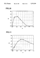
- FIGS. 8 to 13 are graphs showing numerically simulated relationships between a conversion efficiency rate and a quantity ⁇ for the Gunn diodes having said one exemplary configuration of FIG. 7 with various settings summarized in the table 1.
- FIG. 14 is a graph of the quantity ⁇ versus a product NL showing a region of a high conversion efficiency rate obtained from the graphs of FIGS. 8 to 13, for explaining one embodiment of the present invention.
- FIG. 15 is a graph of a distribution of a donor impurity concentration in another exemplary configuration of a Gunn diode according to the present invention.
- FIGS. 16 to 21 are graphs showing numerically simulated relationships between a conversion efficiency rate, a product NL, and a quantity ⁇ for the Gunn diodes having said another exemplary configuration of FIG. 15 with various settings summarized in the table 2.
- FIG. 22 is a graph of a distribution of a donor impurity concentration in still another exemplary configuration of a Gunn diode according to the present invention.
- FIGS. 23 to 25 are graphs showing numerically simulated relationships between a conversion efficiency rate, a product NL, and a quantity ⁇ for the Gunn diodes having said still another exemplary configuration of FIG. 22 with various settings summarized in the table 3.
- FIG. 26 is a graph of the quantity ⁇ versus a product NL showing a region of a high conversion efficiency rate obtained from the graphs of FIGS. 16 to 21 and FIGS. 23 to 25, for explaining one embodiment of the present invention.
- FIG. 27 is a graph showing relationships between a conversion efficiency rate and a quantity ⁇ for the Gunn diodes having said one exemplary configuration of FIG. 7, using two different lattice temperature.
- FIG. 28 is a graph of the quantity ⁇ versus a product NL showing a region of a high conversion efficiency rate obtained from the Gunn diode samples having the exemplary configurations of FIG. 7 and FIG. 15 with various settings summarized in the tables 4 and 5.
- FIGS. 29 to 33 are graphs showing numerically simulated relationships between a conversion efficiency and a quantity ⁇ for the Gunn diodes having said one exemplary configuration of FIG. 7 with various settings summarized in the table 6.
- FIG. 34 is a graph of the quantity ⁇ versus a product NL showing a region of a high conversion efficiency obtained from the graphs of FIGS. 29 to 33, for explaining another embodiment of the present invention.
- a Gunn diode comprising: an n-type active layer made of an InP semiconductor body; and two n + -type layers sandwiching the n-type active layer, each of which is having a donor concentration greater than the n-type active layer and connected with a metallic electrode either directly or indirectly; where the donor impurity concentration in the n-type active layer is graded along a direction perpendicular to a contact plane between the n-type active layer and the n + -type layers, and its average concentration gradient G simultaneously satisfies the following two inequalities:
- L is a thickness of the n-type active layer
- N is an average concentration of the donor impurity
- the donor impurity concentration of the n-type active layer it is preferable for the donor impurity concentration of the n-type active layer to have the substantially constant concentration gradient.
- the donor impurity concentration of the n-type active layer prefferably be constant at a prescribed region neighboring a cathode side end of the n-type active layer and have the substantially constant concentration gradient in the remaining region.
- the thickness L of the n-type active layer is not greater than 2 ⁇ m, and a product NL of the thickness L of the n-type active layer and the average concentration N of the donor impurity to be not greater than 2.0 ⁇ 10 12 cm -2 .
- This configuration has an advantage of preventing the appearance of the dead zone and thereby improving the conversion efficiency without lowering the reliability while maintaining the n + nn + structure, for the reason to be explained in detail below.
- the size of the dead zone can be made smaller by providing an appropriate average concentration gradient G in a direction perpendicular to the contact plane between the n-type active layer 11 and the n + -type layers 12 and 13.
- FIG. 14 The results shown in FIG. 8 to FIG. 13 are summarized in FIG. 14 in which a region in which the conversion efficiency rate Q becomes large is indicated by a shadowed region on a graph of NL on a horizontal axis and a common logarithm of ⁇ on a vertical axis.
- the shadowed region between the straight lines B and C is a region for which the conversion efficiency rate Q takes a value greater than 1.3, and the condition for a given Gunn diode to belong to this region defined by the straight lines B and C is expressed by the inequalities (1) and (2) described above.
- the numerical simulation experiment was conducted to study a dependency of a conversion efficiency rate on Q ⁇ for a group of InP Gunn diodes having a substantially constant impurity concentration Nd(x) for a region in a vicinity of one end of the n-type active layer 11 and a gradient of the impurity concentration Nd(x) which is substantially constant throughout the remaining region of the n-type active layer 11, as shown in FIG. 15, in which case Nd(x) can be expressed as: ##EQU1## where 0 ⁇ 1, and ⁇ , N.sub. ⁇ , ⁇ , and ⁇ are parameters used in the simulation.
- the average concentration gradient G and therefore ⁇ which is related to G through the equation (3), is taken as such a value that for an approximation Nd(x) 1 for the impurity concentration Nd(x) given by:
- FIG. 26 The results shown in FIG. 16 to FIG. 21 and FIG. 23 to FIG. 25 are summarized in FIG. 26 in which a case for which the conversion efficiency rate Q takes a value greater than 1.3 is plotted by a black dot, while a case for which the conversion efficiency rate Q takes a value not greater than 1.3 is plotted by a blank dot, on a graph of NL on a horizontal axis and a common logarithm of ⁇ on a vertical axis.
- FIG. 26 the same straight lines B and C as appeared in FIG. 14 above are also indicated. This FIG.
- an n + -type layer 12 On one side of an n-type InP substrate (with S or Sn dopant, and the impurity concentration of 2 to 5 ⁇ 10 19 cm -3 ), an n + -type layer 12, an n-type active layer 11, and an n + -type layer 13 are epitaxially grown.
- the n + -type layers 12 and 13 are formed to have a thickness of 1.5 ⁇ m each, and the impurity concentration of 1 ⁇ 10 18 cm -3
- the n-type active layer 11 is formed to have a thickness of 1.1 ⁇ m and the average impurity concentration of 1.0 to 1.4 ⁇ 10 16 cm -3 with the impurity concentration distribution given by the equations (4) or (5) described above.
- a first metallic electrode having a double layer structure comprising an ohmic metal layer such as that of AuGe and an Au film is formed.
- the another side of the n-type InP substrate is thinned to make the thickness of the entire Gunn diode to be 10 ⁇ m by using methods such as lapping, polishing, or etching.
- a resist pattern having an opening of 40 ⁇ m diameter is formed by using a photolithography.
- a second metallic electrode having a double layer structure comprising an ohmic metal layer and an Au film is formed by an evaporation of the ohmic metal, a lift-off using the resist pattern, and an Au metal plating.
- the InP Gunn diode manufactured in this manner is then installed into a pill shaped package, and attached inside the waveguide.
- the maximum RF output can then be obtained by applying 4 to 6 V of the DC voltage and taking a matching of cavity impedance.
- the product NL of the average impurity concentration N and the thickness L of the n-type active layer is made larger, the DC input power increases and the heat release becomes difficult, so that it is preferable to make a value of this product NL to be not greater than 2.0 ⁇ 10 12 cm -2 , or more preferably, to be 1.0 to 1.5 ⁇ 10 12 cm -2 .
- the Gunn diodes of the types shown in FIG. 15 and FIG. 22 can also be manufactured in the manner similar to that just described for the Gunn diode of a type shown in FIG. 7, by using the impurity concentration gradient given by the equation (5) or (8) instead of the equation (4) at the step (a) of the above procedure.
- These Gunn diodes have the oscillation frequency of about 94 GHz.
- the Gunn diode is formed such that the donor impurity concentration in the n-type active layer is graded along a direction perpendicular to a contact plane between the n-type active layer and the n + -type layers, and its average concentration gradient G simultaneously satisfies the two inequalities (1) and (2), so that it becomes possible to provide a Gunn diode in which the conversion efficiency can be improved without lowering the reliability, by reducing the dead zone while maintaining n + nn + structure.
- the average concentration gradient G it is also preferable for the average concentration gradient G to simultaneously satisfy the following three inequalities:
- This configuration also has an advantage of preventing the appearance of the dead zone and thereby improving the conversion efficiency without lowering the reliability while maintaining the n + nn + structure, for the reason similar to that explained in detail above.
- ⁇ is taken as positive when the side having the lower donor impurity concentration is used as the cathode side, whereas ⁇ is taken as negative when the side having the lower donor impurity concentration is used as the anode side.
- FIG. 34 The results shown in FIG. 29 to FIG. 33 are summarized in FIG. 34 in which a point of a maximum conversion efficiency is indicated by a blank dot and a range for the conversion efficiency of over 80% of the maximum conversion efficiency is indicated by arrows associated with the blank dot, on a graph of NL on a horizontal axis and a common logarithm of ⁇ on a vertical axis.
- a region between the straight lines D and E can be regarded as a region of the high conversion efficiency, and the condition for a given Gunn diode to belong to this region defined by the straight lines D and E is expressed by the inequalities (9) and (10) described above.
- the inequality (11) expresses the fact that a value of ⁇ is physically limited to be not greater than 1. The fact that the dead zone is actually reduced during the oscillation operation for the Gunn diodes belonging to this region compared with the other Gunn diodes not belonging to this region had been confirmed by the numerical simulations.
- the Gunn diode can also be formed such that the donor impurity concentration in the n-type active layer is graded along a direction perpendicular to a contact plane between the n-type active layer and the n + -type layers, and its average concentration gradient G simultaneously satisfies the three inequalities (9), (10) and (11), so that it becomes possible to provide a Gunn diode in which the conversion efficiency can be improved without lowering the reliability, by removing the dead zone completely, while maintaining n + nn + structure.
- the donor impurity concentration Nd should be considered as a macroscopic quantity obtained by averaging the microscopic donor impurity concentrations over the Debyc length of the conduction electrons, because strictly speaking the microscopic impurity concentration can fluctuate spatially, so that the concentration gradient cannot be controlled as exactly as required by the inequalities (1) and (2) or (9) to (11) on a microscopic level.
Landscapes
- Electrodes Of Semiconductors (AREA)
Abstract
Description
G>(A.sub.1 N/L)exp(-NL/S.sub.1) (1)
G<(A.sub.2 N/L)exp(-NL/S.sub.2) (2)
α=GL/(2N) (3)
Nd(x)=N[1+2α(x/L-1/2)] (4)
              TABLE 1
______________________________________
FIG. No.      L (μm)
                      N (× 10.sup.16 cm.sup.-3)
______________________________________
 8            0.8     3.0
 9            1.1     1.2
10            1.5     2.0
11            1.2     1.4
12            1.1     0.6
13            1.0     1.0
______________________________________
              TABLE 2
______________________________________
FIG. No.  L (μm)
                  Nφ (× 10.sup.16 cm.sup.-3)
                                 β
                                      γ
______________________________________
16        1.1     1.2            0.05 0.1
17        1.1     1.2            0.10 0.1
18        1.1     1.2            0.15 0.1
19        1.1     1.2            0.10 0.5
20        1.1     1.2            0.25 0.1
21        1.1     1.2            0.20 0.1
______________________________________
Nd(x).sub.1 =N[1+2α(x/L-1/2)] (6)
Nd(x)=N.sub.φ (1+μexp[kx/L]) (8)
              TABLE 3
______________________________________
FIG. No.  L (μm)   N.sub.φ (× 10.sup.16 cm.sup.-3)
                                   μ
______________________________________
23        1.1         0.5          0.5
24        1.1         0.5          1.0
25        1.1         0.2          1.0
______________________________________
              TABLE 4
______________________________________
        L        N.sub.φ
Diode No.
        (μm)  (× 10.sup.16 cm.sup.-3)
                             β
                                   γ
                                         ρ
______________________________________
1       1.1      1.2         0     0     0
2       1.1      1.4         0     0     0
3       1.1      1.2         0     0     0.125
4       1.1      1.4         0     0     0.125
5       1.1      1.2         0     0     0.250
6       1.1      1.4         0     0     0.250
7       1.1      1.2         0.091 0     0.250
8       1.1      1.2         0.091 0     0.375
9       1.1      1.3         0     0     0.375
10      1.1      1.0         0.091 0     0.25
11      1.1      1.2         0     0     0.5
12      1.1      1.4         0     0     0.5
13      1.1      1.0         0     0     0
14      1.1      1.0         0     0     0.125
15      1.1      1.0         0     0     0.25
16      1.1      1.0         0     0     0.5
______________________________________
              TABLE 5
______________________________________
Diode eff    N (× 10.sup.16       NL (x × 10.sup.12
No.   (%)    cm.sup.-3)
                       α
                             Q    Z     cm.sup.-2)
______________________________________
1     1.5    1.2       0     1    0     1.32
2     1.4    1.4       0     1    0     1.54
3     1.6    1.2       0.125 1.07 0     1.32
4     1.8    1.4       0.125 1.29 0     1.54
5     2.6    1.2       0.250 1.73 0     1.32
6     2.8    1.4       0.250 2.00 0     1.54
7     2.4    1.11      0.498 (1.6)
                                  0.050 1.22
8     2.9    1.12      0.593 (1.9)
                                  0.041 1.23
9     2.6    1.3       0.375 (1.7)
                                  0     1.43
10    2.3    0.92      0.498 1.78 0.050 1.01
11    1.8    1.2       0.5   1.20 0     1.32
12    1.5    1.4       0.5   1.07 0     1.54
13    1.3    1.0       0     1    0     1.1
14    1.7    1.0       0.125 1.31 0     1.1
15    1.2    1.0       0.250 0.9  0     1.1
16    1.1    1.0       0.5   0.85 0     1.1
______________________________________
G>(A.sub.1 N/L)exp(-NL/S.sub.3) (9)
G<(A.sub.3 N/L)exp(-NL/S.sub.4) (10)
G<2N/L (11)
              TABLE 6
______________________________________
FIG.   L         N           Oscillation
No.    (μm)   (× 10.sup.16 cm.sup.-3)
                             Frequency (GHz)
______________________________________
29     1.0       1.8         94
30     1.0       3.6         94
31     1.0       2.6         94
32     1.2       1.8         78
33     1.1       0.6         118
______________________________________
Claims (10)
G>(A.sub.1 N/L)exp(-NL/S.sub.1)
G<(A.sub.2 N/L)exp(-NL/S.sub.2)
G>(A.sub.1 N/L)exp(-NL/S.sub.3)
G<(A.sub.3 N/L)exp(-NL/S.sub.4)
G<2N/L
Applications Claiming Priority (2)
| Application Number | Priority Date | Filing Date | Title |
|---|---|---|---|
| JP13545590 | 1990-05-28 | ||
| JP2-135455 | 1990-05-28 |
Publications (1)
| Publication Number | Publication Date |
|---|---|
| US5311034A true US5311034A (en) | 1994-05-10 |
Family
ID=15152115
Family Applications (1)
| Application Number | Title | Priority Date | Filing Date |
|---|---|---|---|
| US07/705,673 Expired - Fee Related US5311034A (en) | 1990-05-28 | 1991-05-24 | Indium phosphide Gunn diode with dopant gradient |
Country Status (1)
| Country | Link |
|---|---|
| US (1) | US5311034A (en) |
Cited By (3)
| Publication number | Priority date | Publication date | Assignee | Title |
|---|---|---|---|---|
| US20060153426A1 (en) * | 2003-06-24 | 2006-07-13 | Koninklijke Philips Electronics, N.V. | Method of moving a device provided with a camera to a desired position by means of a control system, and such a system |
| US20100163837A1 (en) * | 2007-02-09 | 2010-07-01 | Technische Universitaet Darmstadt | Gunn diode |
| RU2456715C1 (en) * | 2011-04-01 | 2012-07-20 | Открытое акционерное общество "Научно-исследовательский институт полупроводниковых приборов" (ОАО "НИИПП") | Gunn diode |
-
1991
- 1991-05-24 US US07/705,673 patent/US5311034A/en not_active Expired - Fee Related
Non-Patent Citations (16)
| Title |
|---|
| A. Yokohata et al., "Millimeter-Wave InP Gunn diodes with Linearly Graded Profiles Grown by Low Pressure MOCVD", Sep. 18-21, 1990, The 3rd Asia-Pacific Microwave Conference Proceedings, pp. 1135-1138. |
| A. Yokohata et al., Millimeter Wave InP Gunn diodes with Linearly Graded Profiles Grown by Low Pressure MOCVD , Sep. 18 21, 1990, The 3rd Asia Pacific Microwave Conference Proceedings, pp. 1135 1138. * |
| F. B. Frank et al., "High Efficiency Millimetre Wave Oscillators and Amplifiers", Electronic Engineering, Jun. 1985, pp. 39-42. |
| F. B. Frank et al., High Efficiency Millimetre Wave Oscillators and Amplifiers , Electronic Engineering, Jun. 1985, pp. 39 42. * |
| H. Kurita et al., "W-Band InP Gunn Diodes with Optimized Linearly Graded Doping Profiles", Apr. 1991, Conference Digest, p. 81. |
| H. Kurita et al., W Band InP Gunn Diodes with Optimized Linearly Graded Doping Profiles , Apr. 1991, Conference Digest, p. 81. * |
| J. M. Szubert et al., "W-Band GaAs Gunn Diodes with High Output Power", Sep. 1990, Solid-State Electronics, vol. 33, No. 8, pp. 1035-1037. |
| J. M. Szubert et al., W Band GaAs Gunn Diodes with High Output Power , Sep. 1990, Solid State Electronics, vol. 33, No. 8, pp. 1035 1037. * |
| John Ondria and Raymond L. Ross, "Enhanced Ted MMW Device Performance Using Graded Doping Profiles", Sep. 1987, 17th European Microwave Conference, pp. 673-680. |
| John Ondria and Raymond L. Ross, "Improved Performance of Fundamental and Second Harmonic MMW Oscillators Through Active Device Doping Concentration Contouring", 1987, IEEE MTT-S Digest, pp. 977-980. |
| John Ondria and Raymond L. Ross, "Improved Performance of Fundamental and Second Harmonic MMW Oscillators Through Active Doping Concentration Contouring", 1987, IEEE MTT-S Digest, pp. 977-980. |
| John Ondria and Raymond L. Ross, Enhanced Ted MMW Device Performance Using Graded Doping Profiles , Sep. 1987, 17th European Microwave Conference, pp. 673 680. * |
| John Ondria and Raymond L. Ross, Improved Performance of Fundamental and Second Harmonic MMW Oscillators Through Active Device Doping Concentration Contouring , 1987, IEEE MTT S Digest, pp. 977 980. * |
| John Ondria and Raymond L. Ross, Improved Performance of Fundamental and Second Harmonic MMW Oscillators Through Active Doping Concentration Contouring , 1987, IEEE MTT S Digest, pp. 977 980. * |
| S. M. Sze, "Physics of Semiconductor Devices, Second Edition", 1981, pp. 646 and 649. |
| S. M. Sze, Physics of Semiconductor Devices, Second Edition , 1981, pp. 646 and 649. * |
Cited By (3)
| Publication number | Priority date | Publication date | Assignee | Title |
|---|---|---|---|---|
| US20060153426A1 (en) * | 2003-06-24 | 2006-07-13 | Koninklijke Philips Electronics, N.V. | Method of moving a device provided with a camera to a desired position by means of a control system, and such a system |
| US20100163837A1 (en) * | 2007-02-09 | 2010-07-01 | Technische Universitaet Darmstadt | Gunn diode |
| RU2456715C1 (en) * | 2011-04-01 | 2012-07-20 | Открытое акционерное общество "Научно-исследовательский институт полупроводниковых приборов" (ОАО "НИИПП") | Gunn diode |
Similar Documents
| Publication | Publication Date | Title |
|---|---|---|
| US5705847A (en) | Semiconductor device | |
| US4410902A (en) | Planar doped barrier semiconductor device | |
| US4551905A (en) | Fabrication of metal lines for semiconductor devices | |
| US5250815A (en) | Hot electron injector Gunn device with anode heat sink | |
| Kamoua et al. | D-band (110–170 GHz) InP gunn devices | |
| US5258624A (en) | Transferred electron effect device | |
| US5311034A (en) | Indium phosphide Gunn diode with dopant gradient | |
| US4673960A (en) | Fabrication of metal lines for semiconductor devices | |
| US4855796A (en) | Beam lead mixer diode | |
| EP0161016B1 (en) | Semiconductor laser | |
| US3990099A (en) | Planar Trapatt diode | |
| US4442445A (en) | Planar doped barrier gate field effect transistor | |
| US20060232347A1 (en) | Gunn diode | |
| Gronqvist et al. | A millimeter wave quantum well diode oscillator | |
| Chao et al. | 0.2 micron length T-shaped gate fabrication using angle evaporation | |
| EP0235248B1 (en) | Detector and mixer diode operative at zero bias voltage and fabrication process therefor | |
| Sherrill et al. | Interfacial stress and excess noise in Schottky-barrier mixer diodes | |
| EP0343737B1 (en) | A transferred electron effect device | |
| US5665999A (en) | Metal-semiconductor diode and process for preparing metal-semiconductor diodes | |
| JP2633103B2 (en) | Gun diode | |
| GB2064868A (en) | Schottky barrier gate field-effect transistor | |
| Kim et al. | Characteristics of an area-variable varactor diode | |
| Shino et al. | GaAs power MESFETs prepared by metalorganic chemical vapour deposition | |
| JP4030622B2 (en) | Gunn diode | |
| JP2647631B2 (en) | Semiconductor device |
Legal Events
| Date | Code | Title | Description |
|---|---|---|---|
| AS | Assignment |
Owner name: NIPPON MINING CO., LTD., JAPAN Free format text: ASSIGNMENT OF ASSIGNORS INTEREST.;ASSIGNORS:KURITA, HIROSHI;YOKOHATA, AKIHITO;KODAMA, ATSUSHI;AND OTHERS;REEL/FRAME:005760/0145 Effective date: 19910610 |
|
| AS | Assignment |
Owner name: JAPAN ENERGY CORPORATION, JAPAN Free format text: CHANGE OF NAME EFFECTIVE ON 12/01/1993.;ASSIGNOR:NIPPON MINING CO., LTD.;REEL/FRAME:006865/0892 Effective date: 19940126 |
|
| FEPP | Fee payment procedure |
Free format text: PAYOR NUMBER ASSIGNED (ORIGINAL EVENT CODE: ASPN); ENTITY STATUS OF PATENT OWNER: LARGE ENTITY |
|
| FPAY | Fee payment |
Year of fee payment: 4 |
|
| REMI | Maintenance fee reminder mailed | ||
| LAPS | Lapse for failure to pay maintenance fees | ||
| STCH | Information on status: patent discontinuation |
Free format text: PATENT EXPIRED DUE TO NONPAYMENT OF MAINTENANCE FEES UNDER 37 CFR 1.362 |
|
| FP | Lapsed due to failure to pay maintenance fee |
Effective date: 20020510 |