US5259061A - Fabrication and phase tuning of an optical waveguide device - Google Patents
Fabrication and phase tuning of an optical waveguide device Download PDFInfo
- Publication number
- US5259061A US5259061A US07/976,742 US97674292A US5259061A US 5259061 A US5259061 A US 5259061A US 97674292 A US97674292 A US 97674292A US 5259061 A US5259061 A US 5259061A
- Authority
- US
- United States
- Prior art keywords
- optical waveguide
- optical
- waveguide
- phase angle
- laser
- Prior art date
- Legal status (The legal status is an assumption and is not a legal conclusion. Google has not performed a legal analysis and makes no representation as to the accuracy of the status listed.)
- Expired - Lifetime
Links
Images


Classifications
-
- G—PHYSICS
- G02—OPTICS
- G02B—OPTICAL ELEMENTS, SYSTEMS OR APPARATUS
- G02B6/00—Light guides; Structural details of arrangements comprising light guides and other optical elements, e.g. couplings
- G02B6/10—Light guides; Structural details of arrangements comprising light guides and other optical elements, e.g. couplings of the optical waveguide type
- G02B6/12—Light guides; Structural details of arrangements comprising light guides and other optical elements, e.g. couplings of the optical waveguide type of the integrated circuit kind
- G02B6/12007—Light guides; Structural details of arrangements comprising light guides and other optical elements, e.g. couplings of the optical waveguide type of the integrated circuit kind forming wavelength selective elements, e.g. multiplexer, demultiplexer
-
- G—PHYSICS
- G02—OPTICS
- G02B—OPTICAL ELEMENTS, SYSTEMS OR APPARATUS
- G02B6/00—Light guides; Structural details of arrangements comprising light guides and other optical elements, e.g. couplings
- G02B6/10—Light guides; Structural details of arrangements comprising light guides and other optical elements, e.g. couplings of the optical waveguide type
- G02B6/12—Light guides; Structural details of arrangements comprising light guides and other optical elements, e.g. couplings of the optical waveguide type of the integrated circuit kind
- G02B6/122—Basic optical elements, e.g. light-guiding paths
- G02B6/125—Bends, branchings or intersections
-
- G—PHYSICS
- G02—OPTICS
- G02F—OPTICAL DEVICES OR ARRANGEMENTS FOR THE CONTROL OF LIGHT BY MODIFICATION OF THE OPTICAL PROPERTIES OF THE MEDIA OF THE ELEMENTS INVOLVED THEREIN; NON-LINEAR OPTICS; FREQUENCY-CHANGING OF LIGHT; OPTICAL LOGIC ELEMENTS; OPTICAL ANALOGUE/DIGITAL CONVERTERS
- G02F1/00—Devices or arrangements for the control of the intensity, colour, phase, polarisation or direction of light arriving from an independent light source, e.g. switching, gating or modulating; Non-linear optics
- G02F1/01—Devices or arrangements for the control of the intensity, colour, phase, polarisation or direction of light arriving from an independent light source, e.g. switching, gating or modulating; Non-linear optics for the control of the intensity, phase, polarisation or colour
- G02F1/21—Devices or arrangements for the control of the intensity, colour, phase, polarisation or direction of light arriving from an independent light source, e.g. switching, gating or modulating; Non-linear optics for the control of the intensity, phase, polarisation or colour by interference
- G02F1/225—Devices or arrangements for the control of the intensity, colour, phase, polarisation or direction of light arriving from an independent light source, e.g. switching, gating or modulating; Non-linear optics for the control of the intensity, phase, polarisation or colour by interference in an optical waveguide structure
-
- G—PHYSICS
- G02—OPTICS
- G02F—OPTICAL DEVICES OR ARRANGEMENTS FOR THE CONTROL OF LIGHT BY MODIFICATION OF THE OPTICAL PROPERTIES OF THE MEDIA OF THE ELEMENTS INVOLVED THEREIN; NON-LINEAR OPTICS; FREQUENCY-CHANGING OF LIGHT; OPTICAL LOGIC ELEMENTS; OPTICAL ANALOGUE/DIGITAL CONVERTERS
- G02F2203/00—Function characteristic
- G02F2203/20—Intrinsic phase difference, i.e. optical bias, of an optical modulator; Methods for the pre-set thereof
Definitions
- the present invention relates generally to waveguide fabrication and in particular to the adjustment of the phase angle of an optical waveguide device.
- phase angle is important.
- the phase angle in optical waveguide devices must be precise for optimum performance, e.g., directional couplers require phase matching and a precise coupling length for proper performance and Mach-Zehnder interferometers require an optical phase difference of 90° between the arms of the interferometer for linear operation.
- the precise achievement of the required phase angle is very hard to obtain since phase velocity in optical devices depends on material indices and waveguide geometry.
- Another object is to precisely adjust the phase angle of an optical waveguide device after manufacture to obtain a different phase angle from the original phase angle.
- the accumulated phase angle along the waveguide is adjusted by removing optical waveguide material through laser ablation. Due to the change in optical waveguide geometry in the ablated region, a change in optical phase velocity results, thereby affecting the optical path length in that section of the waveguide. As a result, the output phase angle of the device is changed and is subject to instantaneous measurement. If measurement subsequent to the initial laser ablation determines that the desired phase angle is not present at the output of the device, the ablation procedure is repeated until the precise adjustment is achieved. In multiple channel devices, precise adjustment of the output phase angle of any such device can be achieved by tuning each device in turn by its required amount.
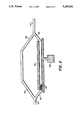
- FIG. 1 shows an arrangement for performing laser ablation and monitoring phase angle of an optical waveguide device.
- FIG. 2 shows a view, partially in section, of an interferometric modulator configuration, with a laser-ablated section.
- FIG. 3 shows the change in phase bias, ⁇ 0 , (dashed line) and depth of material removed (solid line), per pulse, as a function of laser fluence on the substrate of the interferometric modulator.
- FIG. 1 The system of the present invention for phase tuning an optical waveguide device is shown in FIG. 1, along with the interconnection of various components necessary for precise phase tuning of singlemode channel optical waveguide devices during or after fabrication.
- An optical waveguide device 12 to be phase-tuned is placed on a positioning stage 14 within the aperture 13 of an ablating laser beam 42 whose aperture is controllable to a micrometer, or less, resolution by beam shaping shutters 36 and attached to a voltage source 16.
- a signal source laser 18 is connected to an input 22 of the device 12 by a polarization-preserving input fiber optic cable 24. (The frequency of the signal generated by the signal source laser 18 is immaterial to the invention).
- a detector 28 capable of measuring the laser signal at the output 26 of the device 12, is connected by a fiber optic cable 32 to the device 12.
- an oscilloscope 34 is attached to the detector 28.
- the ablating laser beam 42 is aligned with a segment of the optical waveguide fiber in the device 12 selected for ablation and shaped utilizing beam shaping shutters 36 and a focusing lens element 38. Positioning of the laser beam 42 is done so as not to have any of the supporting structure of the device 12 within the focus of the laser beam 42.
- the output phase angle or bias, ⁇ 0 is measured. After one pulse of laser exposure by the ablating laser 42 , ⁇ 0 is remeasured. Variations in the change of output phase angle, ⁇ 0 , due to ablation are achieved either by changing the energy of the laser beam 42 or shifting the locus of the laser beam 42 along the optical waveguide fiber to an undisturbed segment, or both.
- Ablating lasers with good ablation characteristics are essential to the tuning process. Because the excimer laser beam has an appropriate ultraviolet (uV) wavelength to achieve ablation (material removal without heating), it is preferred. Shaping of the ablating laser beam geometry by the use of precision shutters 36, to a micrometer or less, permits precise positioning of the ablating laser beam 42 on the waveguide section 54 to be ablated. Variation of the ablating laser 42 energy/pulse permits the removal of a very small amount of the optical waveguide 54. Because the invention permits the monitoring of small changes in phase resulting from this removal, the invention can iteratively and controllably trim the output phase of the optical waveguide, as desired.
- uV ultraviolet
- ablation refers to the removal of material from the surface of the optical waveguide channel by wearing away, erosion, melting, vaporization without heating of the surface of the optical waveguide material.
- An area ablated is, in this instance, a 4 by 160 ⁇ m area 54 of one side of a channel waveguide (arm) 46.
- laser trimming could be performed on lengths of the interferometer waveguide channels 44,46 before the electrode 48 section.
- the Mach-Zehnder Interferometer 12 was fiber-coupled and packaged in a box 56, the lid of which was not sealed so that access to the optical channel surface was possible.
- a 1.3 ⁇ m laser source 42 coupled to the interferometer input 22 was switched on and the output 26 power coupled 32 to a detector 28 which was monitored using an oscilloscope 34.
- a ⁇ 1 kHz voltage source 16 was connected by a cable 58 to the modulator electrodes 48,52.
- the Mach-Zehnder 12 was placed on a positioning stage 14 under an excimer laser beam 42.
- the laser beam 42 was shaped and aligned so as to expose a certain area 54 of one waveguide arm 46 (typically 4 ⁇ 160 ⁇ m 2 ). With the laser 42 positioned, the output phase angle, ⁇ 0 , was measured. After a one pulse laser exposure or event, ⁇ 0 was remeasured and found to be greater than the desired ⁇ 0 of 90°. To move ⁇ 0 toward the desired 90°, a further length of the same arm 46 was exposed to the pulse laser event. (If the phase angle change, ⁇ 0 , after ablation exceeds the desired value, a segment located on the other optical waveguide channel 44 is ablated, and the above steps are repeated until the desired value of the phase angle ⁇ is achieved.)
- phase angle, ⁇ 0 A quantitative change in phase angle, due to ablation was varied by changing laser energy.
- single pulse laser 42 exposures, each over an area of 4 by 160 ⁇ m 2 were made on portions of each interferometer arm 44,46.
- results of this experiment when graphically represented, as shown in FIG. 3, show a relationship of laser fluence to the amount of material removed 62 and the change of phase angle, ⁇ 0 , per laser pulse 64.
- the depth of material removed is measured in an area of blank LiNbO 3 exposed to 100 pulses and is the average depth trimmed per pulse. (The depth per pulse varies from 0.036 to 0.069 ⁇ m.)
- the ⁇ 0 is measured for one pulse of 4 ⁇ 160 ⁇ m 2 beam size.
- Angle changes of ⁇ 0.8° to 8° are achieved for fluences of 1.1 to 3.5 J/cm 2 . At fluences of greater than ⁇ 3 J/cm 2 , the magnitude of the change in angle appeared to saturate.
- the measurement method used has a ⁇ 0.5° error; angle determinations based on the measured relative harmonic contents of the modulated light give greater accuracy.
- a Mach-Zehnder Interferometer with an initial phase angle of 102° was first tuned to 116° by a two pulse exposure on one arm 46. Several exposures on the other arm 44 decreased the angle to 90° ( ⁇ 0.5° measurement error). For the last pulse the exposed area 54 was 4 ⁇ 90 ⁇ m 2 , a length being chosen from calibration of previous angle changes. Typically, the excimer laser 42 fluence used was ⁇ 2.6 J/cm 2 at the 248 nm wavelength. After tuning ⁇ 0 remained stable at its new value. The total loss in the Mach-Zehnder Interferometer 12 was observed to be 0.5 dB greater than before the laser ablation. Most of the loss occurred with just the first pulse; subsequent ablations, which each joined on the edge of the previous one along the arm 44, caused much smaller increases in loss.
- optical waveguide devices such as the interferometric waveguide amplitude modulator shown in Burns, can be fabricated and tuned during the production of the device without rejection of devices failing to meet the output phase requirements specified. This results in more reliability and far less waste of materials due to poor production runs.
- the excimer laser can be precisely shaped and positioned, no photolithographic processing is required.
- the trimming process is optically monitored and in-situ measurement of phase bias angle and subsequent correction are performed. Because of this controllability, one can trim the output phase angle of optical waveguides devices, simply, during manufacture and thereafter.
- phase angle tuning is performed on any optical waveguide device whose operating point depends on waveguide phase velocity, e.g., interferometers, directional couplers, 1 ⁇ 2 directional couplers, linear voltage sensors and digital optical switches, etc.
- the phases of any devices on the same substrate can be tuned individually, each device being tuned by a different amount depending on the correction required.
- This allows arrays of optical waveguide devices, such as optimally linear modulators (or modulators with any other desired phase characteristics), to be fabricated on one substrate. Because of the advantages of excimer laser ablation over the prior art, the invention can produce the necessary trimming of such optical waveguides in far less time, thus further increasing the efficiency with which one can manufacture optical waveguide devices.
- phase tuning approach of this invention facilitates the fabrication and use of optical waveguide devices.
- the invention is shown in what is considered to be the most practical and preferred embodiment, and is done so for purposes of illustration rather than limitation.
- the invention is presently of interest in the production of Mach-Zehnder Interferometers, it is also used for directional couplers and other such devices previously enumerated, in accordance with any material system which absorbs an appropriate wavelength, e.g., ultra violet.
Landscapes
- Physics & Mathematics (AREA)
- General Physics & Mathematics (AREA)
- Optics & Photonics (AREA)
- Engineering & Computer Science (AREA)
- Microelectronics & Electronic Packaging (AREA)
- Nonlinear Science (AREA)
- Optical Integrated Circuits (AREA)
Abstract
Description
Claims (2)
Priority Applications (1)
| Application Number | Priority Date | Filing Date | Title |
|---|---|---|---|
| US07/976,742 US5259061A (en) | 1991-09-27 | 1992-11-16 | Fabrication and phase tuning of an optical waveguide device |
Applications Claiming Priority (2)
| Application Number | Priority Date | Filing Date | Title |
|---|---|---|---|
| US07/766,939 US5195163A (en) | 1991-09-27 | 1991-09-27 | Fabrication and phase tuning of an optical waveguide device |
| US07/976,742 US5259061A (en) | 1991-09-27 | 1992-11-16 | Fabrication and phase tuning of an optical waveguide device |
Related Parent Applications (1)
| Application Number | Title | Priority Date | Filing Date |
|---|---|---|---|
| US07/766,939 Division US5195163A (en) | 1991-09-27 | 1991-09-27 | Fabrication and phase tuning of an optical waveguide device |
Publications (1)
| Publication Number | Publication Date |
|---|---|
| US5259061A true US5259061A (en) | 1993-11-02 |
Family
ID=27117824
Family Applications (1)
| Application Number | Title | Priority Date | Filing Date |
|---|---|---|---|
| US07/976,742 Expired - Lifetime US5259061A (en) | 1991-09-27 | 1992-11-16 | Fabrication and phase tuning of an optical waveguide device |
Country Status (1)
| Country | Link |
|---|---|
| US (1) | US5259061A (en) |
Cited By (3)
| Publication number | Priority date | Publication date | Assignee | Title |
|---|---|---|---|---|
| WO2000048024A1 (en) * | 1999-02-12 | 2000-08-17 | The University Of Sydney | Laser ablation of waveguide structures |
| US20030077040A1 (en) * | 2001-10-22 | 2003-04-24 | Patel C. Kumar N. | Optical bit stream reader system |
| US7194162B2 (en) | 2002-02-22 | 2007-03-20 | Neophotonics Corporation | Filter response optimization for an arrayed waveguide grating device by adjusting grating optical path length at nanometer scale |
Citations (2)
| Publication number | Priority date | Publication date | Assignee | Title |
|---|---|---|---|---|
| US4266850A (en) * | 1980-01-28 | 1981-05-12 | The United States Of America As Represented By The Secretary Of The Navy | Integrated bias for waveguide amplitude modulator |
| US5059763A (en) * | 1990-06-06 | 1991-10-22 | Massachusetts Institute Of Technology | Formation of optical quality surfaces in optical material |
-
1992
- 1992-11-16 US US07/976,742 patent/US5259061A/en not_active Expired - Lifetime
Patent Citations (2)
| Publication number | Priority date | Publication date | Assignee | Title |
|---|---|---|---|---|
| US4266850A (en) * | 1980-01-28 | 1981-05-12 | The United States Of America As Represented By The Secretary Of The Navy | Integrated bias for waveguide amplitude modulator |
| US5059763A (en) * | 1990-06-06 | 1991-10-22 | Massachusetts Institute Of Technology | Formation of optical quality surfaces in optical material |
Non-Patent Citations (6)
| Title |
|---|
| Brannon et al., Excimer Laser Etching of Polyimide, J. Appl. Phys., 58 (5), 1 Sep. 1985, pp. 2036 2043. * |
| Brannon et al., Excimer Laser Etching of Polyimide, J. Appl. Phys., 58 (5), 1 Sep. 1985, pp. 2036-2043. |
| C. H. Bulmer, Sensitive, Highly Linear Lithium Niobate Interferometers For Electromagnetic Field Sensing, Appl. Phys. Lett. 53(24), 12 Dec. 1988, pp. 2368 2370. * |
| C. H. Bulmer, Sensitive, Highly Linear Lithium Niobate Interferometers Forlectromagnetic Field Sensing, Appl. Phys. Lett. 53(24), 12 Dec. 1988, pp. 2368-2370. |
| Howerton et al., Effect of Intrinsic Phase Mismatch on Linear Modulator Performance of the 1 2 Directional Coupler and Mach Zehnder Interferometer, J. of Lgtwave Tech. vol. 8, No. 8, Aug. 1990, pp. 1177 1186. * |
| Howerton et al., Effect of Intrinsic Phase Mismatch on Linear Modulator Performance of the 1×2 Directional Coupler and Mach-Zehnder Interferometer, J. of Lgtwave Tech. vol. 8, No. 8, Aug. 1990, pp. 1177-1186. |
Cited By (7)
| Publication number | Priority date | Publication date | Assignee | Title |
|---|---|---|---|---|
| WO2000048024A1 (en) * | 1999-02-12 | 2000-08-17 | The University Of Sydney | Laser ablation of waveguide structures |
| EP1181588A4 (en) * | 1999-02-12 | 2003-08-06 | Univ Sydney | LASER ABLATION OF WAVEGUIDE STRUCTURES |
| US20030077040A1 (en) * | 2001-10-22 | 2003-04-24 | Patel C. Kumar N. | Optical bit stream reader system |
| US7233739B2 (en) | 2001-10-22 | 2007-06-19 | Patel C Kumar N | Optical bit stream reader system |
| US20070242952A1 (en) * | 2001-10-22 | 2007-10-18 | Patel C Kumar N | Optical bit stream reader system and method |
| US7630633B2 (en) | 2001-10-22 | 2009-12-08 | Patel C Kumar N | Optical bit stream reader system and method |
| US7194162B2 (en) | 2002-02-22 | 2007-03-20 | Neophotonics Corporation | Filter response optimization for an arrayed waveguide grating device by adjusting grating optical path length at nanometer scale |
Similar Documents
| Publication | Publication Date | Title |
|---|---|---|
| US11899229B2 (en) | Method and apparatus for preparing femtosecond optical filament interference direct writing volume grating/chirped volume grating | |
| US7116852B2 (en) | Optical signal processing circuit and method of producing same | |
| KR20110065450A (en) | Adaptive Optic Beamforming in Laser Processing Systems | |
| WO1988009917A1 (en) | Optical modulation and measurement process | |
| JPH10319254A (en) | Forming method of bragg reflection grating in waveguide and bragg reflection grating thereof formed by same method | |
| US6093927A (en) | Automated precision wavelength control for fiber optic Bragg grating writing | |
| US5898804A (en) | Precision wavelength control for automated fiber optic Bragg grating writing | |
| US5195163A (en) | Fabrication and phase tuning of an optical waveguide device | |
| JP2022519822A (en) | Calibration of the focal position of the laser beam | |
| JP2004295066A (en) | Manufacturing method of optical waveguide | |
| US5259061A (en) | Fabrication and phase tuning of an optical waveguide device | |
| DE69126097T2 (en) | Polarization measuring system | |
| CN109387901A (en) | The laser writing device and method of the nano-precision pitch of long-period fiber grating | |
| Bulmer et al. | Phase tuning by laser ablation of LiNbO/sub 3/interferometric modulators to optimum linearity | |
| US6911659B1 (en) | Method and apparatus for fabricating and trimming optical fiber bragg grating devices | |
| JP2005161372A (en) | Laser processing apparatus, structure, optical element, and laser processing method | |
| CA2640710C (en) | Apparatus and method for producing fibre bragg gratings in a waveguide | |
| KR20020003193A (en) | Laser ablation of waveguide structures | |
| US5118923A (en) | Laser annealed optical devices made by the proton exchange process | |
| JPH0321916A (en) | Optical modulator | |
| Bulmer et al. | Phase tuning of LiNbO3 interferometric modulators by laser ablation | |
| US6873762B1 (en) | Fabrication of fiber optic grating apparatus and method | |
| JPH02248903A (en) | Apparatus for controlling and adjusting mode alignment of optical fiber | |
| CN119124041B (en) | A wavelength customizable all-fiber MZI sensor and its manufacturing method | |
| JP3555414B2 (en) | Short wavelength light source, optical wavelength conversion element, and inspection method for optical wavelength conversion element |
Legal Events
| Date | Code | Title | Description |
|---|---|---|---|
| STCF | Information on status: patent grant |
Free format text: PATENTED CASE |
|
| FPAY | Fee payment |
Year of fee payment: 4 |
|
| FPAY | Fee payment |
Year of fee payment: 8 |
|
| FPAY | Fee payment |
Year of fee payment: 12 |
|
| AS | Assignment |
Owner name: COMERICA BANK, CALIFORNIA Free format text: INTELLECTUAL PROPERTY SECURITY AGREEMENT;ASSIGNOR:COVEGA CORPORATION;REEL/FRAME:015766/0083 Effective date: 20050210 |
|
| FEPP | Fee payment procedure |
Free format text: PAYOR NUMBER ASSIGNED (ORIGINAL EVENT CODE: ASPN); ENTITY STATUS OF PATENT OWNER: LARGE ENTITY |
|
| AS | Assignment |
Owner name: COVEGA CORPORATION, NEW JERSEY Free format text: RELEASE BY SECURED PARTY;ASSIGNOR:COMERICA BANK;REEL/FRAME:022416/0253 Effective date: 20090317 |
|
| AS | Assignment |
Owner name: THORLABS QUANTUM ELECTRONICS, INC., NEW JERSEY Free format text: ASSIGNMENT OF ASSIGNORS INTEREST;ASSIGNOR:COVEGA CORPORATION;REEL/FRAME:022427/0994 Effective date: 20090317 |