US5258759A - Method and apparatus for monotonic algorithmic digital-to-analog and analog-to-digital conversion - Google Patents
Method and apparatus for monotonic algorithmic digital-to-analog and analog-to-digital conversion Download PDFInfo
- Publication number
- US5258759A US5258759A US07/962,451 US96245192A US5258759A US 5258759 A US5258759 A US 5258759A US 96245192 A US96245192 A US 96245192A US 5258759 A US5258759 A US 5258759A
- Authority
- US
- United States
- Prior art keywords
- holding means
- charge
- charge holding
- analog
- digital
- Prior art date
- Legal status (The legal status is an assumption and is not a legal conclusion. Google has not performed a legal analysis and makes no representation as to the accuracy of the status listed.)
- Expired - Lifetime
Links
- 238000006243 chemical reaction Methods 0.000 title claims abstract description 69
- 238000000034 method Methods 0.000 title claims abstract description 36
- 230000010076 replication Effects 0.000 claims abstract description 40
- 239000003990 capacitor Substances 0.000 claims description 36
- 238000012546 transfer Methods 0.000 claims description 20
- 230000006870 function Effects 0.000 claims description 18
- 230000003213 activating effect Effects 0.000 claims description 12
- 238000012935 Averaging Methods 0.000 claims description 6
- 238000002347 injection Methods 0.000 claims description 2
- 239000007924 injection Substances 0.000 claims description 2
- 230000003362 replicative effect Effects 0.000 claims 8
- 230000008878 coupling Effects 0.000 claims 3
- 238000010168 coupling process Methods 0.000 claims 3
- 238000005859 coupling reaction Methods 0.000 claims 3
- 238000005516 engineering process Methods 0.000 abstract description 17
- 230000008569 process Effects 0.000 abstract description 10
- 230000010354 integration Effects 0.000 abstract description 4
- 230000006835 compression Effects 0.000 abstract description 3
- 238000007906 compression Methods 0.000 abstract description 3
- 238000009966 trimming Methods 0.000 abstract description 3
- 125000004122 cyclic group Chemical class 0.000 description 5
- 238000001228 spectrum Methods 0.000 description 5
- 101150061829 bre-3 gene Proteins 0.000 description 3
- 238000010586 diagram Methods 0.000 description 3
- 238000013507 mapping Methods 0.000 description 3
- 238000012545 processing Methods 0.000 description 3
- 230000004075 alteration Effects 0.000 description 2
- 230000015654 memory Effects 0.000 description 2
- 238000007792 addition Methods 0.000 description 1
- 230000008859 change Effects 0.000 description 1
- 230000000295 complement effect Effects 0.000 description 1
- 230000003247 decreasing effect Effects 0.000 description 1
- 238000013461 design Methods 0.000 description 1
- 230000001939 inductive effect Effects 0.000 description 1
- 238000005192 partition Methods 0.000 description 1
- 238000005070 sampling Methods 0.000 description 1
- 239000004065 semiconductor Substances 0.000 description 1
- 239000007787 solid Substances 0.000 description 1
Images


Classifications
-
- G—PHYSICS
- G11—INFORMATION STORAGE
- G11C—STATIC STORES
- G11C16/00—Erasable programmable read-only memories
- G11C16/02—Erasable programmable read-only memories electrically programmable
- G11C16/06—Auxiliary circuits, e.g. for writing into memory
- G11C16/34—Determination of programming status, e.g. threshold voltage, overprogramming or underprogramming, retention
- G11C16/3418—Disturbance prevention or evaluation; Refreshing of disturbed memory data
-
- G—PHYSICS
- G11—INFORMATION STORAGE
- G11C—STATIC STORES
- G11C11/00—Digital stores characterised by the use of particular electric or magnetic storage elements; Storage elements therefor
- G11C11/56—Digital stores characterised by the use of particular electric or magnetic storage elements; Storage elements therefor using storage elements with more than two stable states represented by steps, e.g. of voltage, current, phase, frequency
- G11C11/565—Digital stores characterised by the use of particular electric or magnetic storage elements; Storage elements therefor using storage elements with more than two stable states represented by steps, e.g. of voltage, current, phase, frequency using capacitive charge storage elements
-
- G—PHYSICS
- G11—INFORMATION STORAGE
- G11C—STATIC STORES
- G11C16/00—Erasable programmable read-only memories
- G11C16/02—Erasable programmable read-only memories electrically programmable
- G11C16/06—Auxiliary circuits, e.g. for writing into memory
- G11C16/34—Determination of programming status, e.g. threshold voltage, overprogramming or underprogramming, retention
- G11C16/3418—Disturbance prevention or evaluation; Refreshing of disturbed memory data
- G11C16/3431—Circuits or methods to detect disturbed nonvolatile memory cells, e.g. which still read as programmed but with threshold less than the program verify threshold or read as erased but with threshold greater than the erase verify threshold, and to reverse the disturbance via a refreshing programming or erasing step
-
- G—PHYSICS
- G11—INFORMATION STORAGE
- G11C—STATIC STORES
- G11C27/00—Electric analogue stores, e.g. for storing instantaneous values
-
- G—PHYSICS
- G11—INFORMATION STORAGE
- G11C—STATIC STORES
- G11C27/00—Electric analogue stores, e.g. for storing instantaneous values
- G11C27/02—Sample-and-hold arrangements
- G11C27/024—Sample-and-hold arrangements using a capacitive memory element
-
- H—ELECTRICITY
- H03—ELECTRONIC CIRCUITRY
- H03M—CODING; DECODING; CODE CONVERSION IN GENERAL
- H03M1/00—Analogue/digital conversion; Digital/analogue conversion
- H03M1/12—Analogue/digital converters
- H03M1/34—Analogue value compared with reference values
- H03M1/38—Analogue value compared with reference values sequentially only, e.g. successive approximation type
- H03M1/46—Analogue value compared with reference values sequentially only, e.g. successive approximation type with digital/analogue converter for supplying reference values to converter
- H03M1/464—Non-linear conversion
-
- H—ELECTRICITY
- H03—ELECTRONIC CIRCUITRY
- H03M—CODING; DECODING; CODE CONVERSION IN GENERAL
- H03M1/00—Analogue/digital conversion; Digital/analogue conversion
- H03M1/66—Digital/analogue converters
- H03M1/664—Non-linear conversion not otherwise provided for in subgroups of H03M1/66
-
- G—PHYSICS
- G11—INFORMATION STORAGE
- G11C—STATIC STORES
- G11C7/00—Arrangements for writing information into, or reading information out from, a digital store
- G11C7/16—Storage of analogue signals in digital stores using an arrangement comprising analogue/digital [A/D] converters, digital memories and digital/analogue [D/A] converters
Definitions
- the present invention relates to converting digital information to analog information and vice versa. More particularly, the present invention relates to a compact architecture, suitable for use in semiconductor technology to implement a robust monotonic algorithmic digital-to-analog converter and a corresponding successive approximation analog-to-digital converter.
- an algorithmic digital-to-analog (D/A) converter converts a digital word to its corresponding analog quantity, such as a voltage, in a sequence starting with the least significant bit (LSB) of the digital word and terminating with the most significant bit (MSB).
- LSB least significant bit
- MSB most significant bit
- Another disadvantage to the traditional algorithmic D/A converters is that the digital word is processed in a bit sequence from the LSB to the MSB, whereas for analog-to-digital conversion the bits of the digital word necessarily proceed from the MSB to the LSB.
- the intermediate D/A conversion results cannot serve as successive approximations for A/D conversion because the order in which the bits are processed are different for the two conversions.
- the sequence of bits in the D/A conversion needs to start with the MSB and to terminate with the LSB.
- a cyclic A/D converter avoids this problem by utilizing an algorithm which avoids the need for successive approximations.
- the cyclic A/D converter does not inherently perform D/A conversion, and the final analog approximation value, representative of the converted digital word, is not explicitly available. This is a disadvantage in certain applications, requiring bi-directional conversion between the analog and digital domains.
- the D/A and A/D converters utilize a number of elements with analogues in various technology environments.
- the elements include four charge-holding means, one switch for charge sharing, and two "bi-directional replication elements" for charge storage and recall.
- a specific embodiment of the bi-directional replication element suitable for implementation in CMOS technology is provided.
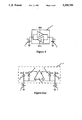
- FIG. 1 shows the tree structure tracing the sequences of intermediate states for digital-to-analog conversion in accordance with the method of the present invention.
- FIG. 2 shows a sequence of intermediate steps in processing a particular example following the digital-to-analog conversion method in accordance with the present invention.
- FIG. 3 illustrates schematically the concept of a bi-directional replication element which is utilized in accordance with the present invention.
- FIGS. 4(a)-4(b) illustrate a CMOS implementation as one embodiment of the bi-directional replication element in accordance with the present invention.
- FIGS. 5(a)-5(b) show the block diagram and a specific CMOS implementation of a digital-to-analog converter utilizing bi-directional replication elements in accordance with one embodiment of the present invention.
- FIGS. 6(a)-6(b) show the block diagram and a specific CMOS implementation of an analog-to-digital converter which utilizes the digital-to-analog converter of the present invention.
- FIG. 7 illustrates conversion transfer characteristic curves for various values of the capacitor ratio utilized in alternative embodiments of the present invention.
- FIGS. 8(a)-8(b) show the block diagram and a specific CMOS implementation of a combined digital-to-analog and analog-to-digital converter with matched conversion characteristics in accordance with another embodiment of the present invention.
- Each of the values for any given intermediate state U i branches into two possible values for the subsequent state U i+1 , the lower one corresponding to a "0" value of the bit being converted, and the higher one to a "1".
- the arrows in the graph indicate an algorithmic means of constructing the value of the state U i+1 from the values of two previous states, generated in previous iterations of the conversion process.
- the solid arrows denote the contribution to the value of state U i by the value of the previous state U i-1
- the broken arrows denote the contribution to the value of U i by the value of one of the earlier states, selected by the polarity of bit i.
- the value of U i is constructed simply by averaging the values of the two selected generating states.
- a practical conversion algorithm can be formulated, involving three analog "registers" U, U + and U - that are updated at every bit cycle i. To do so, it is necessary to introduce initialization values U ref + and U ref - defining the conversion range of the analog domain; U ref + and U ref - roughly correspond to the upper and lower limit of the analog spectrum respectively.
- the resulting D/A conversion algorithm can be defined in symbolic form as follows:
- bit i is "1": set U i + to U i-1 + and U i - to U i-1 ;
- the intermediate analog states evolve from an initial value halfway between U ref - and U ref + to the final U 4 value.
- This conversion is monotonic in nature because it implements the branching tree structure of FIG. 1, preserving the proper sequence in the analog spectra for all of the intermediate states U i by due selection of the values for the pivots U i - and U i + .
- This guaranteed monotonicity is true even if the intermediate states U i are not set exactly halfway in between the pivots U i - and U i + , provided the deviation from the medium value is consistent.
- the present invention may be implemented in a variety of VLSI technologies, such as CMOS or CCD, each of which will vary the specific component structure. Because the specific technology chosen to implement the invention is irrelevant to the operation, the functional elements are defined in the following general form:
- a “charge holding means” The “size” or area of the device relates the total stored electrical charge to the planar charge density.
- charge holding means refers to one of the terminals of a capacitor, with the other terminal shorted at a fixed potential. The voltage across the capacitor is directly related to the amount of charge held by its capacitance.
- charge holding means will be substituted for the term “capacitor” in the further description below, nevertheless bearing in mind the generality of the device hereby referred to.
- Switch An element, called a "switch", for uniting the charge held by two capacitors whenever the switch is active, effectively redistributing the charge over both capacitors with equal charge density.
- the partition of the total charge among the two capacitors is determined by the ratio of the sizes of the two capacitors.
- FIG. 3 illustrates a BRE 3 coupled to two capacitors 1 and 2.
- the BRE 3 has two active states of operation: “store” (STO) and “recall” (RCL).
- STO store
- RCL recall
- the STO mode the charge Q 1 on capacitor 1 is sensed non-destructively and stored in the form of a charge Q 2 on capacitor 2.
- Q 2 f(Q 1 ) with f a strictly monotonic function.
- the stored charge Q 2 on capacitor 2 is sensed non-destructively and recalled as charge Q 1 on capacitor 1.
- Q 1 g(Q 2 ) with g strictly monotonic.
- An element for comparing the amount of charge on a capacitor with a threshold, and assigning a value "1" to the output bit if the amount of charge is smaller than that threshold, and a value of "0" otherwise.
- FIG. 4(a) One embodiment CMOS implementation of the BRE 3 of FIG. 3 that has a zero recall error, independent of process errors, is shown in FIG. 4(a).
- the circuit consists of a differential operational transconductance amplifier (OTA) 4 with inverting and non-inverting high-impedance outputs. Coupled to OTA 4 are STO switch 5 and RCL switch 6.
- the circuit may optionally include dummy switches 7 and 8 for compensation of charge injection due to clock feed-through in switches 5 and 6.
- FIG. 4(b) A possible transistor-level schematic of the BRE shown in FIG. 4(a) with a simple topology is illustrated in FIG. 4(b).
- the circuit comprises four capacitors, C -' 9, C - 10, C + 11, and C +' 12, one switch SH 13, and two bi-directional replication elements, BRE - 14 and BRE + 15, in accordance with the above description.
- the switch 13 and capacitors 10 and 11 serve the purpose of constructing a charge representing U i by averaging charges representing U i + and U i - .
- BRE - 14 with capacitor 9, as well as BRE + 15 with capacitor 12 function as analog charge storage registers for U i + and U i - respectively, able to store present values of U i for later recall.
- the loop error of successive store and recall operations by the bi-directional replication elements, inducing an offset in the register values, is the main source of error which affects the conversion differential linearity, and hence should be minimized as specified above.
- the conversion algorithm translates in the following D/A conversion method, depicted symbolically below:
- the converted charge is represented by either of Q - on C - 10 or Q + on C + 11.
- the precharging procedure of the initialization step can be performed in a number of ways, e.g., by charging capacitor 10 to Q ref - , capacitor 11 to Q ref + , with Q ref - being less than Q ref + , and then activating both BRE - 14 and BRE - 15 in STO mode.
- capacitor 9 can be charged to Q - ref' and BRE - 14 activated in RCL mode instead, or capacitor 12 can be charged to Q + ref' and BRE + 15 activated in RCL mode.
- FIG. 5(b) which also includes switches 51-54 assisting in the precharging procedure.
- the A/D converter comprises the D/A converter shown in FIG. 5(a) being further coupled to a comparator 16 which receives the analog input for conversion to a digital word. Coupled to either of the capacitors 10 and 11, the comparator senses the intermediate D/A conversion results which serve as the successive approximation values for comparison with the analog input. The results of comparison determine the digital output word in a sequence from MSB to LSB. In turn, the output bits synchronously feed into the D/A converter so as to provide the successive approximations. More specifically, the method of A/D conversion with the circuit of FIG. 6(a) consists of the following sequence of instructions:
- the digital word is given by the sequence of the bits from b) in the order processed, the MSB first and the LSB last.
- the replication and charge sharing instructions can be omitted, as by then the final bit has been determined.
- the instructions following the assignment of the LSB value should be completed in case the final approximation analog value, corresponding to the converted digital word, is required.
- FIG. 6(b) shows a possible transistor-level CMOS implementation of the A/D converter of the invention, based on the D/A converter embodiment of FIG. 5(b).
- the comparator circuit 16 contains a cross-coupled transistor output stage for latched operation; a high pulse on the RST gate 61 triggers the comparison and fixes the output D.OUT at the falling pulse edge.
- the present invention may be implemented in various technologies and with different component structures.
- the references to charge in the above description apply equally to voltage.
- the charge holding devices can be characterized as "capacitors" in the true sense of the term.
- Examples of embodiments of the invention implemented in CMOS technology with capacitive analogues for the charge holding devices are given in FIGS. 5(b) and 6(b).
- the detailed component structure of these circuits allows for countless variations that each may address different performance requirements, such as speed, compactness, power, accuracy, and etc.
- A/D conversion scheme of the invention Another attractive feature concerns the successive-approximation A/D conversion scheme of the invention.
- the combination of concurrent A/D and D/A conversion operations in a single architecture provides the final successive approximation as an analog output along with the digital conversion output.
- the value of this analog output one value for each digital output of the converter, corresponds to the typical, ideal analog quantity at the converter input yielding that digital output.
- the analog output of the combined converter maps an arbitrary analog input value to its closest discrete value, with the spectrum of discrete outputs determined by the resolution and operational range of the converter.
- This discretization property proves very useful in e.g., the implementation of noise-tolerant dynamic refresh schemes for multi-valued analog capacitive memories.
- Self-refreshing analog memories incorporating capacitor banks and the A/D converters of the present invention, can be constructed with limited additional circuitry.
- Such circuitry serves to overwrite, at a given instant, the voltage across a selected capacitor with the final approximation voltage obtained from an A/D conversion of the voltage across that capacitor prior to refresh.
- a useful feature directly related to the previous one concerns the versatility of the converter apparatus, capable of performing both A/D and D/A conversions within a single structure.
- the D/A converter internal to the A/D converter of FIG. 6 can in principle be addressed individually.
- bi-directional conversion of data between the analog and digital domains is possible with this invention.
- the combined A/D and D/A converter of the invention is especially attractive as it provides almost perfectly matched transfer characteristics for conversion between both formats, in analog and digital directions.
- the comparator output may be complemented with an extra inverting high-impedance transconductance output, as shown in FIG. 8(a).
- Such output allows a negative feedback connection to the analog input node A.IN of comparator 16 providing an analog output which matches the input offset of the comparator when the connection is established.
- a possible detailed structure for the resulting combined A/D and D/A converter in CMOS technology based on the structures of FIGS. 5(b) and 6(b), is shown in FIG. 8(b).
- the ENAD logic signal and its complement control the operation mode of the converter: A/D conversion mode (D.OUT active; latched comparator enabled) is achieved when ENAD is high; D/A conversion mode (A.OUT active; negative feedback enabled) is obtained with ENAD low.
Landscapes
- Engineering & Computer Science (AREA)
- Physics & Mathematics (AREA)
- Nonlinear Science (AREA)
- Theoretical Computer Science (AREA)
- Computer Hardware Design (AREA)
- Analogue/Digital Conversion (AREA)
Abstract
Description
______________________________________
Q.sub.ref' .sup.- = f.sup.- (Q.sub.ref.sup.-)
                 Q.sub.ref.sup.-  = g.sup.- (Q.sub.ref'.sup.-));
Q.sub.ref'.sup.+ (Q.sub.ref.sup.+  = g.sup.+ (Q.sub.ref'.sup.+)); and
Q.sub.ref.sup.-  < Q.sub.ref.sup.+
______________________________________
Claims (16)
Priority Applications (2)
| Application Number | Priority Date | Filing Date | Title |
|---|---|---|---|
| US07/962,451 US5258759A (en) | 1992-10-16 | 1992-10-16 | Method and apparatus for monotonic algorithmic digital-to-analog and analog-to-digital conversion |
| US08/146,660 US5479170A (en) | 1992-10-16 | 1993-11-02 | Method and apparatus for long-term multi-valued storage in dynamic analog memory |
Applications Claiming Priority (1)
| Application Number | Priority Date | Filing Date | Title |
|---|---|---|---|
| US07/962,451 US5258759A (en) | 1992-10-16 | 1992-10-16 | Method and apparatus for monotonic algorithmic digital-to-analog and analog-to-digital conversion |
Related Child Applications (1)
| Application Number | Title | Priority Date | Filing Date |
|---|---|---|---|
| US08/146,660 Continuation-In-Part US5479170A (en) | 1992-10-16 | 1993-11-02 | Method and apparatus for long-term multi-valued storage in dynamic analog memory |
Publications (1)
| Publication Number | Publication Date |
|---|---|
| US5258759A true US5258759A (en) | 1993-11-02 |
Family
ID=25505887
Family Applications (1)
| Application Number | Title | Priority Date | Filing Date |
|---|---|---|---|
| US07/962,451 Expired - Lifetime US5258759A (en) | 1992-10-16 | 1992-10-16 | Method and apparatus for monotonic algorithmic digital-to-analog and analog-to-digital conversion |
Country Status (1)
| Country | Link |
|---|---|
| US (1) | US5258759A (en) |
Cited By (13)
| Publication number | Priority date | Publication date | Assignee | Title |
|---|---|---|---|---|
| US5357251A (en) * | 1988-03-23 | 1994-10-18 | Central Institute For The Deaf | Electronic filters, signal conversion apparatus, hearing aids and methods |
| US5589832A (en) * | 1994-12-02 | 1996-12-31 | Lucent Technologies Inc. | Low noise non-sampled successive approximation |
| US5815439A (en) * | 1996-04-30 | 1998-09-29 | Agate Semiconductor, Inc. | Stabilization circuits and techniques for storage and retrieval of single or multiple digital bits per memory cell |
| US5929796A (en) * | 1997-04-29 | 1999-07-27 | National Semiconductor Corporation | Self-calibrating reversible pipeline analog to digital and digital to analog converter |
| US5977812A (en) * | 1998-05-08 | 1999-11-02 | Lsi Logic Corporation | Circuit and method for providing a generally log logarithmic transfer function |
| US6282145B1 (en) | 1999-01-14 | 2001-08-28 | Silicon Storage Technology, Inc. | Array architecture and operating methods for digital multilevel nonvolatile memory integrated circuit system |
| US6285598B1 (en) | 1997-03-06 | 2001-09-04 | Silicon Storage Technology, Inc. | Precision programming of nonvolatile memory cells |
| US6396742B1 (en) | 2000-07-28 | 2002-05-28 | Silicon Storage Technology, Inc. | Testing of multilevel semiconductor memory |
| US6462986B1 (en) | 1995-10-06 | 2002-10-08 | Silicon Storage Technology, Inc. | Integrated circuit for storage and retrieval of multiple digital bits per nonvolatile memory cell |
| US6487116B2 (en) | 1997-03-06 | 2002-11-26 | Silicon Storage Technology, Inc. | Precision programming of nonvolatile memory cells |
| US20070216561A1 (en) * | 2004-07-06 | 2007-09-20 | Kenet, Inc. | Voltage random access memory (VRAM) |
| US7283077B2 (en) | 2005-05-19 | 2007-10-16 | Korea Advanced Institute Of Science And Technology | Divide-add circuit and high-resolution digital-to-analog converter using the same |
| US9998137B1 (en) * | 2016-09-19 | 2018-06-12 | Marvell International Ltd. | Power-efficient successive-approximation analog-to-digital converter using LSB averaging |
Citations (4)
| Publication number | Priority date | Publication date | Assignee | Title |
|---|---|---|---|---|
| US4065766A (en) * | 1976-03-18 | 1977-12-27 | General Electric Company | Analog-to-digital converter |
| US4070667A (en) * | 1975-11-03 | 1978-01-24 | General Electric Company | Charge transfer analog-to-digital converter |
| US4072939A (en) * | 1976-03-01 | 1978-02-07 | International Business Machines Corporation | Analog-to-digital and digital-to-analog converter circuits employing charge redistribution |
| US4144526A (en) * | 1976-01-22 | 1979-03-13 | Siemens Aktiengesellschaft | Circuit arrangement and operating process for converting an analogue signal into a digital signal |
-
1992
- 1992-10-16 US US07/962,451 patent/US5258759A/en not_active Expired - Lifetime
Patent Citations (4)
| Publication number | Priority date | Publication date | Assignee | Title |
|---|---|---|---|---|
| US4070667A (en) * | 1975-11-03 | 1978-01-24 | General Electric Company | Charge transfer analog-to-digital converter |
| US4144526A (en) * | 1976-01-22 | 1979-03-13 | Siemens Aktiengesellschaft | Circuit arrangement and operating process for converting an analogue signal into a digital signal |
| US4072939A (en) * | 1976-03-01 | 1978-02-07 | International Business Machines Corporation | Analog-to-digital and digital-to-analog converter circuits employing charge redistribution |
| US4065766A (en) * | 1976-03-18 | 1977-12-27 | General Electric Company | Analog-to-digital converter |
Cited By (22)
| Publication number | Priority date | Publication date | Assignee | Title |
|---|---|---|---|---|
| US5357251A (en) * | 1988-03-23 | 1994-10-18 | Central Institute For The Deaf | Electronic filters, signal conversion apparatus, hearing aids and methods |
| US5589832A (en) * | 1994-12-02 | 1996-12-31 | Lucent Technologies Inc. | Low noise non-sampled successive approximation |
| US6462986B1 (en) | 1995-10-06 | 2002-10-08 | Silicon Storage Technology, Inc. | Integrated circuit for storage and retrieval of multiple digital bits per nonvolatile memory cell |
| US5815439A (en) * | 1996-04-30 | 1998-09-29 | Agate Semiconductor, Inc. | Stabilization circuits and techniques for storage and retrieval of single or multiple digital bits per memory cell |
| US5901089A (en) * | 1996-04-30 | 1999-05-04 | Agate Semiconductor, Inc. | Stabilization circuits and techniques for storage and retrieval of single or multiple digital bits per memory cell |
| US6487116B2 (en) | 1997-03-06 | 2002-11-26 | Silicon Storage Technology, Inc. | Precision programming of nonvolatile memory cells |
| US6285598B1 (en) | 1997-03-06 | 2001-09-04 | Silicon Storage Technology, Inc. | Precision programming of nonvolatile memory cells |
| US5929796A (en) * | 1997-04-29 | 1999-07-27 | National Semiconductor Corporation | Self-calibrating reversible pipeline analog to digital and digital to analog converter |
| US5977812A (en) * | 1998-05-08 | 1999-11-02 | Lsi Logic Corporation | Circuit and method for providing a generally log logarithmic transfer function |
| US8432750B2 (en) | 1999-01-14 | 2013-04-30 | Silicon Storage Technology, Inc. | Non-volatile memory systems and methods including page read and/or configuration features |
| US6282145B1 (en) | 1999-01-14 | 2001-08-28 | Silicon Storage Technology, Inc. | Array architecture and operating methods for digital multilevel nonvolatile memory integrated circuit system |
| US20070159904A1 (en) * | 1999-01-14 | 2007-07-12 | Tran Hieu V | Wide dynamic range and high speed voltage mode sensing for a multilevel digital non-volatile memory |
| US7471581B2 (en) | 1999-01-14 | 2008-12-30 | Silicon Storage Technology, Inc. | Wide dynamic range and high speed voltage mode sensing for a multilevel digital non-volatile memory |
| US20090147579A1 (en) * | 1999-01-14 | 2009-06-11 | Silicon Storage Technology, Inc. | Non-volatile memory systems and methods including page read and/or configuration features |
| US7848159B2 (en) | 1999-01-14 | 2010-12-07 | Silicon Storage Technology, Inc. | Non-volatile memory systems and methods including page read and/or configuration features |
| US8614924B2 (en) | 1999-01-14 | 2013-12-24 | Silicon Storage Technology, Inc. | Non-volatile memory systems and methods |
| US9640263B2 (en) | 1999-01-14 | 2017-05-02 | Silicon Storage Technology, Inc. | Non-volatile memory systems and methods |
| US6396742B1 (en) | 2000-07-28 | 2002-05-28 | Silicon Storage Technology, Inc. | Testing of multilevel semiconductor memory |
| US20070216561A1 (en) * | 2004-07-06 | 2007-09-20 | Kenet, Inc. | Voltage random access memory (VRAM) |
| EP1784917A4 (en) * | 2004-07-06 | 2008-07-02 | Kenet Inc | Voltage random access memory (vram) |
| US7283077B2 (en) | 2005-05-19 | 2007-10-16 | Korea Advanced Institute Of Science And Technology | Divide-add circuit and high-resolution digital-to-analog converter using the same |
| US9998137B1 (en) * | 2016-09-19 | 2018-06-12 | Marvell International Ltd. | Power-efficient successive-approximation analog-to-digital converter using LSB averaging |
Similar Documents
| Publication | Publication Date | Title |
|---|---|---|
| US5258759A (en) | Method and apparatus for monotonic algorithmic digital-to-analog and analog-to-digital conversion | |
| US8081097B2 (en) | Analog-to-digital converter and related calibrating comparator | |
| US4529965A (en) | Switched-capacitor circuit analog-to-digital converter | |
| US5574457A (en) | Switched capacitor gain stage | |
| US7812757B1 (en) | Hybrid analog-to-digital converter (ADC) with binary-weighted-capacitor sampling array and a sub-sampling charge-redistributing array for sub-voltage generation | |
| KR101689053B1 (en) | A/d converter | |
| US8416107B1 (en) | Charge compensation calibration for high resolution data converter | |
| US9319033B1 (en) | Ramp voltage generator and method for testing an analog-to-digital converter | |
| US5929796A (en) | Self-calibrating reversible pipeline analog to digital and digital to analog converter | |
| US20090073018A1 (en) | High Speed High Resolution ADC Using Successive Approximation Technique | |
| US20180159549A1 (en) | Input Circuit for a Dynamic Comparator | |
| Tong et al. | A 10-Bit 120 kS/s SAR ADC without reset energy for biomedical electronics | |
| WO2024082732A1 (en) | Analog-to-digital converter integrated with reference voltage generation, and calibration method | |
| JPH01202925A (en) | Converter commonly used for analog/digital-digital/ analog conversion | |
| US20040008133A1 (en) | High linearity digital-to-analog converter | |
| US10476513B1 (en) | SAR ADC with high linearity | |
| WO2018047457A1 (en) | Analog-digital converter, electronic device, and method for controlling analog-digital converter | |
| JP3971663B2 (en) | AD converter | |
| US10277237B2 (en) | Successive approximation type A/D conversion circuit | |
| CN113625034A (en) | Sampling circuit, sampling array, integrated storage and calculation chip and electronic equipment | |
| US6198313B1 (en) | Infinite sample-and-hold circuit | |
| Rombouts et al. | Capacitor mismatch compensation for the quasi-passive-switched-capacitor DAC | |
| US4983974A (en) | Analog-to-digital conversion by varying both inputs of a comparator utilizing successive approximation | |
| Lei et al. | Analysis on capacitor mismatch and parasitic capacitors effect of improved segmented-capacitor array in SAR ADC | |
| Bienstman et al. | An 8 channel 8b µ P compatible NMOS converter with programmable ranges |
Legal Events
| Date | Code | Title | Description |
|---|---|---|---|
| AS | Assignment |
Owner name: CALIFORNIA INSTITUTE OF TECHNOLOGY, CALIFORNIA Free format text: ASSIGNMENT OF ASSIGNORS INTEREST.;ASSIGNORS:CAUWENBERGHS, GERT;YARIV, AMNON;REEL/FRAME:006288/0692 Effective date: 19921013 |
|
| STCF | Information on status: patent grant |
Free format text: PATENTED CASE |
|
| FEPP | Fee payment procedure |
Free format text: PAYOR NUMBER ASSIGNED (ORIGINAL EVENT CODE: ASPN); ENTITY STATUS OF PATENT OWNER: SMALL ENTITY |
|
| FPAY | Fee payment |
Year of fee payment: 4 |
|
| FEPP | Fee payment procedure |
Free format text: PAYER NUMBER DE-ASSIGNED (ORIGINAL EVENT CODE: RMPN); ENTITY STATUS OF PATENT OWNER: SMALL ENTITY |
|
| FPAY | Fee payment |
Year of fee payment: 8 |
|
| FEPP | Fee payment procedure |
Free format text: PAYER NUMBER DE-ASSIGNED (ORIGINAL EVENT CODE: RMPN); ENTITY STATUS OF PATENT OWNER: SMALL ENTITY Free format text: PAYOR NUMBER ASSIGNED (ORIGINAL EVENT CODE: ASPN); ENTITY STATUS OF PATENT OWNER: SMALL ENTITY |
|
| FPAY | Fee payment |
Year of fee payment: 12 |
|
| AS | Assignment |
Owner name: SYNOPSYS, INC., CALIFORNIA Free format text: ASSIGNMENT OF ASSIGNORS INTEREST;ASSIGNORS:VIRAGE LOGIC CORPORATION;VL C.V.;ARC CORES LIMITED;AND OTHERS;REEL/FRAME:025105/0907 Effective date: 20100902 |