US5186789A - Method of making a cantilever stylus for use in an atomic force microscope - Google Patents

Method of making a cantilever stylus for use in an atomic force microscope Download PDF

Info

Publication number
US5186789A
US5186789A US07/799,993 US79999391A US5186789A US 5186789 A US5186789 A US 5186789A US 79999391 A US79999391 A US 79999391A US 5186789 A US5186789 A US 5186789A
Authority
US
United States
Prior art keywords
film
cantilever
stylus
force microscope
atomic force
Prior art date
Legal status (The legal status is an assumption and is not a legal conclusion. Google has not performed a legal analysis and makes no representation as to the accuracy of the status listed.)
Expired - Lifetime
Application number
US07/799,993
Inventor
Nobuhiro Tsuda
Hirofumi Yamada
Hiroyuki Kado
Takao Tohda
Current Assignee (The listed assignees may be inaccurate. Google has not performed a legal analysis and makes no representation or warranty as to the accuracy of the list.)
National Institute of Advanced Industrial Science and Technology AIST
Panasonic Holdings Corp
Original Assignee
Matsushita Electric Industrial Co Ltd
Agency of Industrial Science and Technology
Priority date (The priority date is an assumption and is not a legal conclusion. Google has not performed a legal analysis and makes no representation as to the accuracy of the date listed.)
Filing date
Publication date
Application filed by Matsushita Electric Industrial Co Ltd, Agency of Industrial Science and Technology filed Critical Matsushita Electric Industrial Co Ltd
Assigned to MATSUSHITA ELECTRIC INDUSTRIAL CO., LTD., AGENCY OF INDUSTRIAL SCIENCE AND TECHNOLOGY reassignment MATSUSHITA ELECTRIC INDUSTRIAL CO., LTD. ASSIGNMENT OF ASSIGNORS INTEREST. Assignors: KADO, HIROYUKI, TOHDA, TAKAO, TSUDA, NOBUHIRO, YAMADA, HIROFUMI
Application granted granted Critical
Publication of US5186789A publication Critical patent/US5186789A/en
Anticipated expiration legal-status Critical
Expired - Lifetime legal-status Critical Current

Links

Images

Classifications

    • GPHYSICS
    • G01MEASURING; TESTING
    • G01QSCANNING-PROBE TECHNIQUES OR APPARATUS; APPLICATIONS OF SCANNING-PROBE TECHNIQUES, e.g. SCANNING PROBE MICROSCOPY [SPM]
    • G01Q60/00Particular types of SPM [Scanning Probe Microscopy] or microscopes; Essential components thereof
    • G01Q60/24AFM [Atomic Force Microscopy] or apparatus therefor, e.g. AFM probes
    • G01Q60/38Probes, their manufacture, or their related instrumentation, e.g. holders

Definitions

  • the present invention relates generally to a method of making a cantilever stylus for use in an atomic force microscope, and more particularly to a method of making a flat-cantilever having a free end, of which an edge is used as a stylus.
  • a scanning tunneling microscope (hereinafter referred to simply as STM) has been developed as an instrument capable of observing the surface of a solid body on the atomic scale.
  • STM scanning tunneling microscope
  • AFM atomic force microscope
  • FIG. 1 depicts a conventional cantilever 1 for use in an atomic force microscope.
  • This cantilever 1 is a flat-cantilever formed of a thin film of SiO 2 or Si 3 N 4 .
  • An edge 2 of the cantilever 1 is used as a stylus.
  • This kind of cantilever is generally made by the use of the photolithography technique.
  • a cantilever for an atomic force microscope generally has a length of about 100 ⁇ m, the thickness thereof must range from 1 to 1.5 ⁇ m in consideration of strength thereof.
  • etching must be performed with respect to a thin film having a thickness of about 1-1.5 ⁇ m.
  • a photoresist has been formed on a thin film of cantilever material such as, for example, SiO 2 or Si 3 N 4
  • etching is performed with respect to the thin film with only a portion thereof covered with the photoresist left.
  • the wet-etching technique is generally employed in this etching and the dry-etching technique is not available because the film of cantilever material is relatively thick for the dry-etching.
  • an edge of the cantilever made in the above-described manner has a radius of curvature of about 1 ⁇ m in a direction parallel to the surface of the cantilever and a radius of curvature greater than it in a direction perpendicular to the surface of the cantilever.
  • An atomic force microscope employing such a cantilever cannot possibly obtain a resolving power on the atomic scale.
  • the present invention has been developed to overcome the above-described disadvantages.
  • a method according to the present invention comprises the steps of:
  • the second film of metallic material to be formed on the first film has a thickness of 1000 ⁇ , the problem of separation would not occur even when a photoresist film is used as a resist for etching the metallic film.
  • Such a thickness can easily be processed by either of the wet-etching technique or the dry-etching technique.
  • the metallic film has superior adhesive properties with respect to a film of cantilever material, as compared with the photoresist film. Accordingly, even if the film of cantilever material is removed 1-1.5 ⁇ m by etching with the metallic film as a resist, the metallic film is subjected to no separation.
  • the method according to the present invention therefore, can provide a high-accuracy cantilever stylus having an edge with a very small radius of curvature.
  • FIG. 1 is a perspective view of a conventional cantilever stylus for use in an atomic force microscope
  • FIGS. 2a to 2d are schematic views explanatory of manufacturing processes according to the present invention.
  • FIG. 3 is a perspective view of a cantilever stylus made by the processes of FIGS. 2a to 2d.
  • FIGS. 2a to 2d processes for manufacturing a cantilever stylus suited for use in an atomic force microscope.
  • Two SiO 2 films 12 each having a thickness of 1.5 ⁇ m were initially formed on respective surfaces of a silicon substrate 11 having a thickness of 300-400 ⁇ m by thermal oxidation.
  • Two Cr films 13 each having a thickness of 1000 ⁇ were then formed on external surfaces of respective SiO 2 films 12 by sputtering.
  • the material of the photoresist films is of the positive type to enhance the accuracy.
  • the substrate 11 was submerged in a mixed solution of cerium ammonium nitrate, perchloric acid, and water so that the Cr films 13 might be subjected to etching with the portions thereof covered with the photoresist films left on respective SiO 2 films 12, as shown in FIG. 2b.
  • the substrate 11 was submerged in a mixed solution of hydrofluoric acid and ammonium fluoride and the SiO 2 films 12 each having a thickness of 1.5 ⁇ m was subjected to etching with respective Cr films 13 acting as resist films. In this way, a cantilever 15 as shown in FIG. 2c was made.
  • the substrate 11 was submerged in a mixed solution of ethylenediamine, catechol, and water having a temperature of 100° C. so that the silicon substrate 11 might be subjected to anisotropic etching from respective surfaces thereof, as shown in FIG. 2d.
  • the cantilever 15 formed an angle of 55° with that surface of the substrate 11 from which part of the substrate 11 was removed by the etching.
  • FIG. 3 depicts a cantilever stylus made through the above-described processes.
  • a V-shaped cantilever stylus 15 having a length of about 100 ⁇ m was made of an SiO 2 film formed on the surface of a silicon substrate 11.
  • a free end 16 of the cantilever stylus 15 had a radius of curvature of 300 ⁇ in a direction parallel to the surface of the substrate 11 and a radius of curvature of 200 ⁇ in a direction perpendicular thereto.
  • Silicon nitride for example Si 3 N 4
  • Si 3 N 4 can be used as a material of the cantilever stylus, as well as silicon oxide.
  • Co, Fe, Al, W, Mo, Ti, Ta, Au, Ag, Pt, Ni, Rh, Zr, Hf, Nb, or the like can be used as a material of the metallic film to be formed on the cantilever material, as well as Cr.
  • These metals have superior adhesive properties with respect to the cantilever material.
  • Cr, Fe, Co, and Ni have particularly superior adhesive properties and therefore were available in making a superior cantilever stylus.
  • the method according to the present invention can provide a cantilever stylus having a tip with a radius of curvature less than 300 ⁇ .
  • the use of such a cantilever stylus is particularly useful for the manufacture of an atomic force microscope having a very high resolving power and capable of observing the surface configuration of various materials including insulators on the atomic scale.

Abstract

A cantilever stylus suited for use in an atomic force microscope is made in the following processes: forming a first film on a substrate; forming a second film of metallic material on an external surface of the first film; forming a photoresist film on an external surface of the second film by making use of a photolithography technique; performing etching with respect to the second film with only a portion thereof covered with the photoresist film left on the first film; and further performing etching with respect to the first film with the second film being used as a resist film so that the first film may be configured into a cantilever stylus.

Description

BACKGROUND OF THE INVENTION
1. Field of the Invention
The present invention relates generally to a method of making a cantilever stylus for use in an atomic force microscope, and more particularly to a method of making a flat-cantilever having a free end, of which an edge is used as a stylus.
2. Description of the Prior Art
Conventionally, a scanning tunneling microscope (hereinafter referred to simply as STM) has been developed as an instrument capable of observing the surface of a solid body on the atomic scale. However, since the STM detects a tunnel current between a sample and a stylus to observe the surface of the sample, it is impossible for the STM to observe the surface of an insulator. In order to solve this problem, an atomic force microscope (hereinafter referred to simply as AFM) for observing the surface of a sample by detecting forces acting between the sample and the stylus has been proposed. Because the AFM detects minute forces, it requires a cantilever having a stylus and a length of about 100 μm. The resolving power of the AFM depends greatly upon the radius of curvature of the stylus. The less the radius of curvature is, the higher is the resolving power.
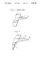
FIG. 1 depicts a conventional cantilever 1 for use in an atomic force microscope. This cantilever 1 is a flat-cantilever formed of a thin film of SiO2 or Si3 N4. An edge 2 of the cantilever 1 is used as a stylus. This kind of cantilever is generally made by the use of the photolithography technique.
Because a cantilever for an atomic force microscope generally has a length of about 100 μm, the thickness thereof must range from 1 to 1.5 μm in consideration of strength thereof. In making such a cantilever, etching must be performed with respect to a thin film having a thickness of about 1-1.5 μm. In an ordinary photolithography process, after a photoresist has been formed on a thin film of cantilever material such as, for example, SiO2 or Si3 N4, etching is performed with respect to the thin film with only a portion thereof covered with the photoresist left. The wet-etching technique is generally employed in this etching and the dry-etching technique is not available because the film of cantilever material is relatively thick for the dry-etching. Even by the use of the wet-etching technique, however, it is likely that such a thickness would cause separation of the photoresist during etching, thereby causing a relatively large under-etching in which that portion of the film of cantilever material from which the photoresist has been separated is excessively etched. As a result, an edge of the cantilever made in the above-described manner has a radius of curvature of about 1 μm in a direction parallel to the surface of the cantilever and a radius of curvature greater than it in a direction perpendicular to the surface of the cantilever. An atomic force microscope employing such a cantilever cannot possibly obtain a resolving power on the atomic scale.
SUMMARY OF THE INVENTION
The present invention has been developed to overcome the above-described disadvantages.
It is accordingly an object of the present invention to provide an improved method of making a cantilever stylus for use in an atomic force microscope, which stylus is capable of observing the surface of a sample on the atomic scale.
In accomplishing this and other objects, a method according to the present invention comprises the steps of:
forming a first film on a substrate;
forming a second film of metallic material on an external surface of the first film, the metallic material being different from a material of the first film;
forming a photoresist film on an external surface of the second film by making use of a photolithography technique;
performing etching with respect to the second film with only a portion thereof covered with the photoresist film left; and
further performing etching with respect to the first film with the second film being used as a resist film so that the first film is configured into a cantilever stylus suited for use in an atomic force microscope.
According to the method of the present invention, because it is sufficient if the second film of metallic material to be formed on the first film has a thickness of 1000 Å, the problem of separation would not occur even when a photoresist film is used as a resist for etching the metallic film. Such a thickness can easily be processed by either of the wet-etching technique or the dry-etching technique.
Furthermore, the metallic film has superior adhesive properties with respect to a film of cantilever material, as compared with the photoresist film. Accordingly, even if the film of cantilever material is removed 1-1.5 μm by etching with the metallic film as a resist, the metallic film is subjected to no separation. The method according to the present invention, therefore, can provide a high-accuracy cantilever stylus having an edge with a very small radius of curvature.
BRIEF DESCRIPTION OF THE DRAWINGS
This and other objects and features of the present invention will become more apparent from the following description taken in conjunction with the preferred embodiment thereof with reference to the accompanying drawings, throughout which like parts are designated by like reference numerals, and wherein:
FIG. 1 is a perspective view of a conventional cantilever stylus for use in an atomic force microscope;
FIGS. 2a to 2d are schematic views explanatory of manufacturing processes according to the present invention; and
FIG. 3 is a perspective view of a cantilever stylus made by the processes of FIGS. 2a to 2d.
DETAILED DESCRIPTION OF THE PREFERRED EMBODIMENT
Referring now to the drawings, there are shown in FIGS. 2a to 2d processes for manufacturing a cantilever stylus suited for use in an atomic force microscope.
Two SiO2 films 12 each having a thickness of 1.5 μm were initially formed on respective surfaces of a silicon substrate 11 having a thickness of 300-400 μm by thermal oxidation. Two Cr films 13 each having a thickness of 1000 Å were then formed on external surfaces of respective SiO2 films 12 by sputtering. After two photoresist films were coated on external surfaces of respective Cr films 13, one of them was configured into a photoresist film 14 in the form of a V-shaped cantilever having a length of about 100 μm by the photolithography technique, as shown in FIG. 2a. The material of the photoresist films is of the positive type to enhance the accuracy.
Thereafter, the substrate 11 was submerged in a mixed solution of cerium ammonium nitrate, perchloric acid, and water so that the Cr films 13 might be subjected to etching with the portions thereof covered with the photoresist films left on respective SiO2 films 12, as shown in FIG. 2b.
Subsequently, the substrate 11 was submerged in a mixed solution of hydrofluoric acid and ammonium fluoride and the SiO2 films 12 each having a thickness of 1.5 μm was subjected to etching with respective Cr films 13 acting as resist films. In this way, a cantilever 15 as shown in FIG. 2c was made.
After the Cr films 13 were removed from respective SiO2 films 12, the substrate 11 was submerged in a mixed solution of ethylenediamine, catechol, and water having a temperature of 100° C. so that the silicon substrate 11 might be subjected to anisotropic etching from respective surfaces thereof, as shown in FIG. 2d. In this case, the cantilever 15 formed an angle of 55° with that surface of the substrate 11 from which part of the substrate 11 was removed by the etching.
FIG. 3 depicts a cantilever stylus made through the above-described processes.
As shown in FIG. 3, a V-shaped cantilever stylus 15 having a length of about 100 μm was made of an SiO2 film formed on the surface of a silicon substrate 11. A free end 16 of the cantilever stylus 15 had a radius of curvature of 300 Å in a direction parallel to the surface of the substrate 11 and a radius of curvature of 200 Å in a direction perpendicular thereto.
During etching of the SiO2 films 12, the radii of curvature could be further reduced by the so-called "overetching".
In this process, although the wet-etching was performed with respect to the Cr films 13, the employment of the dry-etching could further enhance the accuracy. In this case, plasma etching with the use of CCl4 was available.
Silicon nitride, for example Si3 N4, can be used as a material of the cantilever stylus, as well as silicon oxide.
Furthermore, Co, Fe, Al, W, Mo, Ti, Ta, Au, Ag, Pt, Ni, Rh, Zr, Hf, Nb, or the like can be used as a material of the metallic film to be formed on the cantilever material, as well as Cr. These metals have superior adhesive properties with respect to the cantilever material. Of these metals, Cr, Fe, Co, and Ni have particularly superior adhesive properties and therefore were available in making a superior cantilever stylus.
As is clear from the above, the method according to the present invention can provide a cantilever stylus having a tip with a radius of curvature less than 300 Å. The use of such a cantilever stylus is particularly useful for the manufacture of an atomic force microscope having a very high resolving power and capable of observing the surface configuration of various materials including insulators on the atomic scale.
Although the present invention has been fully described by way of examples with reference to the accompanying drawings, it is to be noted here that various changes and modifications will be apparent to those skilled in the art. Therefore, unless such changes and modifications otherwise depart from the spirit and scope of the present invention, they should be construed as being included therein.

Claims (4)

What is claimed is:
1. A method of making a cantilever stylus for use in an atomic force microscope, which comprises the steps of:
forming a first film on a substrate;
forming a second film of metallic material on an external surface of said first film, said metallic material being different from a material of said first film;
forming a photoresist film on an external surface of said second film by making use of a photolithography technique;
performing etching with respect to said second film with only a portion thereof covered with said photoresist film left on said first film; and
further performing etching with respect to said first film with said second film being used as a resist film so that said first film is configured into a cantilever stylus suited for use in an atomic force microscope.
2. The method according to claim 1, wherein said first film is made of silicon oxide.
3. The method according to claim 1, wherein said first film is made of silicon nitride.
4. The method according to claim 1, wherein said second film is made of a material selected from the group consisting of Cr, Fe, Ni, Co, Al, W, Mo, Ti, Ta, Au, Ag, Pt, Rh, Zr, Hf, and Nb.
US07/799,993 1990-11-29 1991-11-29 Method of making a cantilever stylus for use in an atomic force microscope Expired - Lifetime US5186789A (en)

Applications Claiming Priority (2)

Application Number Priority Date Filing Date Title
JP2334024A JP2825973B2 (en) 1990-11-29 1990-11-29 Method of manufacturing cantilever for atomic force microscope
JP2-334024 1990-11-29

Publications (1)

Publication Number Publication Date
US5186789A true US5186789A (en) 1993-02-16

Family

ID=18272651

Family Applications (1)

Application Number Title Priority Date Filing Date
US07/799,993 Expired - Lifetime US5186789A (en) 1990-11-29 1991-11-29 Method of making a cantilever stylus for use in an atomic force microscope

Country Status (4)

Country Link
US (1) US5186789A (en)
EP (1) EP0488133B1 (en)
JP (1) JP2825973B2 (en)
DE (1) DE69107802T2 (en)

Cited By (1)

* Cited by examiner, † Cited by third party
Publication number Priority date Publication date Assignee Title
US5874668A (en) * 1995-10-24 1999-02-23 Arch Development Corporation Atomic force microscope for biological specimens

Families Citing this family (5)

* Cited by examiner, † Cited by third party
Publication number Priority date Publication date Assignee Title
JPH0792173A (en) * 1993-09-24 1995-04-07 Agency Of Ind Science & Technol Cantilever for interatomic force microscope and fabrication thereof
US5509300A (en) * 1994-05-12 1996-04-23 Arizona Board Of Regents Acting For Arizona State University Non-contact force microscope having a coaxial cantilever-tip configuration
JPH08297129A (en) * 1995-04-26 1996-11-12 Nikon Corp Cantilever for interatomic force microscope and its manufacture
DE19519478C2 (en) * 1995-05-27 1997-09-04 Forschungszentrum Juelich Gmbh Manufacturing method for coated tip probe
US5744799A (en) * 1996-05-20 1998-04-28 Ohara; Tetsuo Apparatus for and method of real-time nanometer-scale position measurement of the sensor of a scanning tunneling microscope or other sensor scanning atomic or other undulating surfaces

Citations (1)

* Cited by examiner, † Cited by third party
Publication number Priority date Publication date Assignee Title
US4943719A (en) * 1989-01-17 1990-07-24 The Board Of Trustees Of The Leland Stanford University Microminiature cantilever stylus

Patent Citations (2)

* Cited by examiner, † Cited by third party
Publication number Priority date Publication date Assignee Title
US4943719A (en) * 1989-01-17 1990-07-24 The Board Of Trustees Of The Leland Stanford University Microminiature cantilever stylus
WO1990008397A1 (en) * 1989-01-17 1990-07-26 The Board Of Trustees Of The Leland Stanford Junior University Microminiature cantilever stylus

Non-Patent Citations (10)

* Cited by examiner, † Cited by third party
Title
"CR-P/Si Thin Film Cantilever Structures", IBM Technical Disclosure Bulletin, vol. 33, No. 1B, Jun., 1990.
"Fabrication of Nanostructure by Anisotropic Wet Etching of Silicon", Shimuzu et al., Japanese Journal of Applied Physics, vol. 27, No. 9, Sep. 9, 1988, pp. L1778-L1779.
"Improved Atomic Force Microscope Images Using Microcantilevers with Sharp Tips", Akamine et al., Applied Physics Letters, 57(3), Jul. 16, 1990.
"Microfabrication of Cantilever Styli for the Atomic Force Microscope", Albrecht et al., Journal of Vacuum/Science and Technology, Jul./Aug., No. 4.
"Use of Gold Films as Masks for a KOH Preferential Etch", Ogita et al., Thin Solid Films, 120(1984), pp. L79-81.
CR P/Si Thin Film Cantilever Structures , IBM Technical Disclosure Bulletin, vol. 33, No. 1B, Jun., 1990. *
Fabrication of Nanostructure by Anisotropic Wet Etching of Silicon , Shimuzu et al., Japanese Journal of Applied Physics, vol. 27, No. 9, Sep. 9, 1988, pp. L1778 L1779. *
Improved Atomic Force Microscope Images Using Microcantilevers with Sharp Tips , Akamine et al., Applied Physics Letters, 57(3), Jul. 16, 1990. *
Microfabrication of Cantilever Styli for the Atomic Force Microscope , Albrecht et al., Journal of Vacuum/Science and Technology, Jul./Aug., No. 4. *
Use of Gold Films as Masks for a KOH Preferential Etch , Ogita et al., Thin Solid Films, 120(1984), pp. L79 81. *

Cited By (1)

* Cited by examiner, † Cited by third party
Publication number Priority date Publication date Assignee Title
US5874668A (en) * 1995-10-24 1999-02-23 Arch Development Corporation Atomic force microscope for biological specimens

Also Published As

Publication number Publication date
DE69107802T2 (en) 1995-09-14
DE69107802D1 (en) 1995-04-06
EP0488133A1 (en) 1992-06-03
EP0488133B1 (en) 1995-03-01
JPH04203920A (en) 1992-07-24
JP2825973B2 (en) 1998-11-18

Similar Documents

Publication Publication Date Title
US5239863A (en) Cantilever stylus for use in an atomic force microscope and method of making same
US5399232A (en) Microfabricated cantilever stylus with integrated pyramidal tip
US4943719A (en) Microminiature cantilever stylus
US5021364A (en) Microcantilever with integral self-aligned sharp tetrahedral tip
US5923637A (en) Method of manufacturing micro-tip for detecting tunneling current or micro-force or magnetic force
EP0711029B1 (en) Method of forming a microstructure
US4916002A (en) Microcasting of microminiature tips
JP3370527B2 (en) Atomic force microscope probe, method of manufacturing the same, and atomic force microscope
US6261494B1 (en) Method of forming plastically deformable microstructures
WO2003045838A1 (en) Nano gripper and method of manufacturing the nano gripper
US5186789A (en) Method of making a cantilever stylus for use in an atomic force microscope
EP0646787A1 (en) Cantilever for use with atomic force microscope and process for the production thereof
US6958124B2 (en) SPM sensor and process for producing it
JP3290378B2 (en) Micro mechanical sensor for AFM / STM shape measurement
EP0990195A1 (en) Low-cost photoplastic cantilever
US7119332B2 (en) Method of fabricating probe for scanning probe microscope
JP4686914B2 (en) Manufacturing method of stencil mask
US6858541B2 (en) Etch stop control for MEMS device formation
JPH05203444A (en) Manufacture of cantilever for interatomic force microscope
JPH05296864A (en) Pressure sensor and its manufacture
JPH10300762A (en) Manufacturing method of cantilever
JPH0890431A (en) Microgripper and manufacture thereof
JP2720579B2 (en) Method of manufacturing cantilever for atomic force microscope
JPH0518744A (en) Manufacture of cantilever for atomic force microscope
JPH11340189A (en) Method for forming recess or through hole in micromachine production

Legal Events

Date Code Title Description
AS Assignment

Owner name: AGENCY OF INDUSTRIAL SCIENCE AND TECHNOLOGY, JAPAN

Free format text: ASSIGNMENT OF ASSIGNORS INTEREST.;ASSIGNORS:TSUDA, NOBUHIRO;YAMADA, HIROFUMI;KADO, HIROYUKI;AND OTHERS;REEL/FRAME:005944/0722

Effective date: 19911118

Owner name: MATSUSHITA ELECTRIC INDUSTRIAL CO., LTD., JAPAN

Free format text: ASSIGNMENT OF ASSIGNORS INTEREST.;ASSIGNORS:TSUDA, NOBUHIRO;YAMADA, HIROFUMI;KADO, HIROYUKI;AND OTHERS;REEL/FRAME:005944/0722

Effective date: 19911118

STCF Information on status: patent grant

Free format text: PATENTED CASE

FPAY Fee payment

Year of fee payment: 4

FPAY Fee payment

Year of fee payment: 8

FEPP Fee payment procedure

Free format text: PAYOR NUMBER ASSIGNED (ORIGINAL EVENT CODE: ASPN); ENTITY STATUS OF PATENT OWNER: LARGE ENTITY

FPAY Fee payment

Year of fee payment: 12