US5169791A - Method for the passivation of crystal defects in polycrystalline silicon material - Google Patents
Method for the passivation of crystal defects in polycrystalline silicon material Download PDFInfo
- Publication number
- US5169791A US5169791A US07/585,522 US58552290A US5169791A US 5169791 A US5169791 A US 5169791A US 58552290 A US58552290 A US 58552290A US 5169791 A US5169791 A US 5169791A
- Authority
- US
- United States
- Prior art keywords
- silicon material
- hydrogen
- passivation
- crystal defects
- polycrystalline
- Prior art date
- Legal status (The legal status is an assumption and is not a legal conclusion. Google has not performed a legal analysis and makes no representation as to the accuracy of the status listed.)
- Expired - Fee Related
Links
- 239000002210 silicon-based material Substances 0.000 title claims abstract description 31
- 238000000034 method Methods 0.000 title claims abstract description 26
- 230000007547 defect Effects 0.000 title claims abstract description 22
- 239000013078 crystal Substances 0.000 title claims abstract description 18
- 238000002161 passivation Methods 0.000 title claims abstract description 14
- 229910021420 polycrystalline silicon Inorganic materials 0.000 title claims abstract description 10
- 239000001257 hydrogen Substances 0.000 claims abstract description 11
- 229910052739 hydrogen Inorganic materials 0.000 claims abstract description 11
- UFHFLCQGNIYNRP-UHFFFAOYSA-N Hydrogen Chemical compound [H][H] UFHFLCQGNIYNRP-UHFFFAOYSA-N 0.000 claims abstract description 10
- YZCKVEUIGOORGS-UHFFFAOYSA-N Hydrogen atom Chemical compound [H] YZCKVEUIGOORGS-UHFFFAOYSA-N 0.000 claims abstract description 7
- 229910021417 amorphous silicon Inorganic materials 0.000 claims abstract description 7
- 150000001875 compounds Chemical class 0.000 claims description 8
- XLYOFNOQVPJJNP-UHFFFAOYSA-N water Substances O XLYOFNOQVPJJNP-UHFFFAOYSA-N 0.000 claims description 7
- 239000001301 oxygen Substances 0.000 claims description 6
- 229910052760 oxygen Inorganic materials 0.000 claims description 6
- 230000009467 reduction Effects 0.000 claims description 3
- 230000002349 favourable effect Effects 0.000 abstract description 4
- VYPSYNLAJGMNEJ-UHFFFAOYSA-N Silicium dioxide Chemical compound O=[Si]=O VYPSYNLAJGMNEJ-UHFFFAOYSA-N 0.000 description 4
- 125000004435 hydrogen atom Chemical group [H]* 0.000 description 4
- 239000000463 material Substances 0.000 description 3
- 230000004048 modification Effects 0.000 description 3
- 238000012986 modification Methods 0.000 description 3
- XUIMIQQOPSSXEZ-UHFFFAOYSA-N Silicon Chemical compound [Si] XUIMIQQOPSSXEZ-UHFFFAOYSA-N 0.000 description 2
- 230000003292 diminished effect Effects 0.000 description 2
- 230000000694 effects Effects 0.000 description 2
- 230000006872 improvement Effects 0.000 description 2
- 229910052710 silicon Inorganic materials 0.000 description 2
- 239000010703 silicon Substances 0.000 description 2
- 239000000377 silicon dioxide Substances 0.000 description 2
- 235000012431 wafers Nutrition 0.000 description 2
- 239000011248 coating agent Substances 0.000 description 1
- 238000000576 coating method Methods 0.000 description 1
- 230000001066 destructive effect Effects 0.000 description 1
- 238000009792 diffusion process Methods 0.000 description 1
- 230000003467 diminishing effect Effects 0.000 description 1
- 238000010494 dissociation reaction Methods 0.000 description 1
- 230000005593 dissociations Effects 0.000 description 1
- 238000010438 heat treatment Methods 0.000 description 1
- 150000002431 hydrogen Chemical class 0.000 description 1
- 238000002513 implantation Methods 0.000 description 1
- 238000005215 recombination Methods 0.000 description 1
- 230000006798 recombination Effects 0.000 description 1
- 238000009738 saturating Methods 0.000 description 1
- 230000035945 sensitivity Effects 0.000 description 1
- 235000012239 silicon dioxide Nutrition 0.000 description 1
Images
Classifications
-
- H—ELECTRICITY
- H01—ELECTRIC ELEMENTS
- H01L—SEMICONDUCTOR DEVICES NOT COVERED BY CLASS H10
- H01L21/00—Processes or apparatus adapted for the manufacture or treatment of semiconductor or solid state devices or of parts thereof
- H01L21/02—Manufacture or treatment of semiconductor devices or of parts thereof
- H01L21/04—Manufacture or treatment of semiconductor devices or of parts thereof the devices having at least one potential-jump barrier or surface barrier, e.g. PN junction, depletion layer or carrier concentration layer
- H01L21/18—Manufacture or treatment of semiconductor devices or of parts thereof the devices having at least one potential-jump barrier or surface barrier, e.g. PN junction, depletion layer or carrier concentration layer the devices having semiconductor bodies comprising elements of Group IV of the Periodic System or AIIIBV compounds with or without impurities, e.g. doping materials
- H01L21/30—Treatment of semiconductor bodies using processes or apparatus not provided for in groups H01L21/20 - H01L21/26
- H01L21/3003—Hydrogenation or deuterisation, e.g. using atomic hydrogen from a plasma
-
- Y—GENERAL TAGGING OF NEW TECHNOLOGICAL DEVELOPMENTS; GENERAL TAGGING OF CROSS-SECTIONAL TECHNOLOGIES SPANNING OVER SEVERAL SECTIONS OF THE IPC; TECHNICAL SUBJECTS COVERED BY FORMER USPC CROSS-REFERENCE ART COLLECTIONS [XRACs] AND DIGESTS
- Y10—TECHNICAL SUBJECTS COVERED BY FORMER USPC
- Y10S—TECHNICAL SUBJECTS COVERED BY FORMER USPC CROSS-REFERENCE ART COLLECTIONS [XRACs] AND DIGESTS
- Y10S136/00—Batteries: thermoelectric and photoelectric
- Y10S136/29—Testing, calibrating, treating, e.g. aging
-
- Y—GENERAL TAGGING OF NEW TECHNOLOGICAL DEVELOPMENTS; GENERAL TAGGING OF CROSS-SECTIONAL TECHNOLOGIES SPANNING OVER SEVERAL SECTIONS OF THE IPC; TECHNICAL SUBJECTS COVERED BY FORMER USPC CROSS-REFERENCE ART COLLECTIONS [XRACs] AND DIGESTS
- Y10—TECHNICAL SUBJECTS COVERED BY FORMER USPC
- Y10S—TECHNICAL SUBJECTS COVERED BY FORMER USPC CROSS-REFERENCE ART COLLECTIONS [XRACs] AND DIGESTS
- Y10S148/00—Metal treatment
- Y10S148/128—Proton bombardment of silicon
Definitions
- the present invention is directed to a method for the passivation of crystal defects in polycrystalline or amorphous silicon material using a method that includes a heating step in a hydrogen-containing atmosphere.
- silicon material such as polycrystalline silicon wafers, silicon layers, and silicon materials of arbitrary shapes
- These materials typically include crystal defects such as, for example, point defects or line defects, and offsets or drain boundaries. These crystal defects result in the electronic components manufactured from such silicon material having a diminished quality.
- solar cells or photodiodes that are constructed from a silicon material having a crystal defect exhibit diminished photocurrent sensitivities and no-load voltages as a consequence of increased recombination currents. Unfavorable diode properties occur using such silicon materials.
- the present invention provides a method for the passivation of crystal defects in polycrystalline or amorphous silicon material using a temperature treatment step in a hydrogen-containing atmosphere.
- the method provides favorable diode properties and/or favorable passivation properties in amorphous or, respectively, polycrystalline silicon material in a simple manner.
- the passivation of crystal defects in polycrystalline or amorphous silicon material is achieved using a temperature treatment step in a hydrogen-containing atmosphere wherein hydrogen-oxygen containing compounds are reduced at the surface of the silicon material. Atomic hydrogen is created that diffuses into the silicon material during the method.
- the temperature treatment step is performed at a temperature range of between 250° C, to about 500° C.
- water is used as the hydrogen-oxygen containing compound.
- the method is performed at a pressure that is greater than ambient pressure.
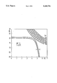
- the Figure illustrates the I-U characteristics of polycrystalline solar cells without an antireflection coat before and after the method of the present invention.
- the present invention is directed to the passivation of crystal defects in amorphous silicon material or polycrystalline material.
- the amorphous silicon material can be used for solar cells, photodiodes, as well as for electrographic recording material.
- the silicon material is heated in a hydrogen-containing atmosphere in the presence of hydrogen-oxygen containing compounds that are reduced at the surface of the silicon material. Atomic hydrogen is created that diffuses into the silicon material.
- the passivation of grain boundaries and of inner-grain defects in the silicon material proceeds by saturating these crystal defects with hydrogen atoms.
- To accomplish the saturation of the defects with hydrogen two steps for generating atomic hydrogen and for transporting it to the crystal defect are necessary.
- a diffusion process is most suitable.
- Hydrogenous compounds whose dissociation energies are lower at defined temperatures than the bonding energy of silicon dioxide (SiO 2 ) are suitable for this purpose.
- SiO 2 silicon dioxide
- the polycrystalline silicon wafers are heated in a water-containing atmosphere. It has been found that a temperature range of between approximately 250° C. to about 500° C. functions satisfactory for the purposes of the present invention.
- the solar cells created from silicon material treated in this manner exhibit improvements in the short-circuit current, no-load voltage, and filling factors.
- the Figure illustrates current-voltage characteristics of polycrystalline solar cells before and after treatment by the method of the present invention in a water-containing atmosphere.
- curve 1 illustrates the current-voltage characteristics of polycrystalline solar cells without antireflection coating before the temperature treatment of the present invention.
- Curve 2 illustrates the current-voltage characteristics of the same polycrystalline solar cell without an antireflection coat after a temperature treatment of the present invention at 330° C. in a water-containing atmosphere for passivation of the crystal defects.
- a comparison of curves 1 and 2 of the Figure clearly demonstrates the improvement achieved by the present invention with respect to the solar cell parameters of "short-circuit" and "no-load voltage".
- the method of the present invention can be performed at ambient pressure. However, the method of the present invention, in an embodiment, can also be performed at elevated pressure in order to achieve a higher passivation effect.
Abstract
A method for the passivation of crystal defects in polycrystalline or amorphous silicon material using a temperature treatment step in a hydrogen-containing atmosphere the method results in favorable diode properties and favorable passivation properties in amorphous or, respectively, polycrystalline silicon material in a simple manner. Hydrogen-oxygen compounds are reduced at the surface of the silicon material, creating atomic hydrogen that diffuses into the silicon material.
Description
The present invention is directed to a method for the passivation of crystal defects in polycrystalline or amorphous silicon material using a method that includes a heating step in a hydrogen-containing atmosphere.
It is known to use silicon material, such as polycrystalline silicon wafers, silicon layers, and silicon materials of arbitrary shapes, to make electronic components. These materials, however, typically include crystal defects such as, for example, point defects or line defects, and offsets or drain boundaries. These crystal defects result in the electronic components manufactured from such silicon material having a diminished quality. For example, solar cells or photodiodes that are constructed from a silicon material having a crystal defect exhibit diminished photocurrent sensitivities and no-load voltages as a consequence of increased recombination currents. Unfavorable diode properties occur using such silicon materials.
Methods, typically referred to as "grain boundary passivation", have been suggested for reducing the effect of these crystal defects. Examples of such methods for reducing the influences of crystal defects include:
a) Implantation of ionized hydrogen atoms: J. E. Johnson, J. I. Hano Ka, and J. A. Gregory, 18. IEEE Photovoltaic Specialists Conference, Las Vegas 1985, pages 1112-1115;
b) Treatment with a hydrogen plasma: W. Schmidt, K. D. Rasch, and K. Roy: 16. IEEE Photovoltaic Specialists Conference, San Diego, 1982, pages 537-542, U.S. Pat. No. 4,835,006; and
c) Temperature treatment in a hydrogen atmosphere: A. Agarwal, D. Bana, and C. M. Singal: Int. I. Electr. 1985, Vol. 58, No. 5, pages 769-774.
The present invention provides a method for the passivation of crystal defects in polycrystalline or amorphous silicon material using a temperature treatment step in a hydrogen-containing atmosphere. The method provides favorable diode properties and/or favorable passivation properties in amorphous or, respectively, polycrystalline silicon material in a simple manner.
To this end, pursuant to the method of the present invention, the passivation of crystal defects in polycrystalline or amorphous silicon material is achieved using a temperature treatment step in a hydrogen-containing atmosphere wherein hydrogen-oxygen containing compounds are reduced at the surface of the silicon material. Atomic hydrogen is created that diffuses into the silicon material during the method.
In an embodiment of the method, the temperature treatment step is performed at a temperature range of between 250° C, to about 500° C.
In an embodiment of the method, water is used as the hydrogen-oxygen containing compound.
In an embodiment of the method, the method is performed at a pressure that is greater than ambient pressure.
Additional features and advantages of the present invention are described in, and will be apparent from, the detailed description of the presently preferred embodiments and from the drawing.
The Figure illustrates the I-U characteristics of polycrystalline solar cells without an antireflection coat before and after the method of the present invention.
The present invention is directed to the passivation of crystal defects in amorphous silicon material or polycrystalline material. The amorphous silicon material can be used for solar cells, photodiodes, as well as for electrographic recording material.
Pursuant to the method of the present invention, the silicon material is heated in a hydrogen-containing atmosphere in the presence of hydrogen-oxygen containing compounds that are reduced at the surface of the silicon material. Atomic hydrogen is created that diffuses into the silicon material.
Pursuant to the present invention, the passivation of grain boundaries and of inner-grain defects in the silicon material proceeds by saturating these crystal defects with hydrogen atoms. To accomplish the saturation of the defects with hydrogen, two steps for generating atomic hydrogen and for transporting it to the crystal defect are necessary. In order to achieve an optimally non-destructive transport of the generated hydrogen atoms to the crystal defect, a diffusion process is most suitable.
Pursuant to the present invention, in order to produce hydrogen atoms, hydrogen-oxygen containing compounds, for example water, are reduced at the surface of the silicon. Hydrogenous compounds whose dissociation energies are lower at defined temperatures than the bonding energy of silicon dioxide (SiO2) are suitable for this purpose. As a consequence of the reduction of the hydrogen-oxygen compounds at the surface of the silicon material, atomic hydrogen is created. The atomic hydrogen is driven into the silicon material to the crystal defects at an appropriate temperature.
By way of example, and not limitation, in an embodiment of the present invention, the polycrystalline silicon wafers are heated in a water-containing atmosphere. It has been found that a temperature range of between approximately 250° C. to about 500° C. functions satisfactory for the purposes of the present invention. The solar cells created from silicon material treated in this manner exhibit improvements in the short-circuit current, no-load voltage, and filling factors.
Referring now to the Figure, the Figure illustrates current-voltage characteristics of polycrystalline solar cells before and after treatment by the method of the present invention in a water-containing atmosphere. In the Figure, curve 1 illustrates the current-voltage characteristics of polycrystalline solar cells without antireflection coating before the temperature treatment of the present invention. Curve 2 illustrates the current-voltage characteristics of the same polycrystalline solar cell without an antireflection coat after a temperature treatment of the present invention at 330° C. in a water-containing atmosphere for passivation of the crystal defects. A comparison of curves 1 and 2 of the Figure clearly demonstrates the improvement achieved by the present invention with respect to the solar cell parameters of "short-circuit" and "no-load voltage".
The method of the present invention can be performed at ambient pressure. However, the method of the present invention, in an embodiment, can also be performed at elevated pressure in order to achieve a higher passivation effect.
It should be understood that various changes and modifications to the presently preferred embodiments described herein will be apparent to those skilled in the art. Such changes and modifications can be made without departing from the spirit and scope of the present invention and without diminishing its attendant advantages. It is therefore intended that such changes and modifications be covered by the appended claims.
Claims (6)
1. A method for the passivation of crystal defects in polycrystalline or amorphous silicon material, comprising the step of:
reducing a compound comprising a hydrogen-oxygen-bond at a surface of the silicon material causing atomic hydrogen to be created that diffuses into the silicon material, the reduction step being performed at a temperature of between approximately 250° C. to about 500° C.
2. The method of claim 1 wherein water is used as the hydrogen-oxygen compound.
3. The method of claim 1 wherein the pressure of an environment containing the bonded hydrogen atmosphere is greater than ambient pressure.
4. A method for the passivation of crystal defects in silicon material comprising the steps of reducing a hydrogen-oxygen containing compound at a surface of a silicon material and causing hydrogen to be created that diffuses into the silicon material, the reduction step being performed at a temperature of between approximately 250° C. to about 500° C.
5. The method of claim 4 wherein water is used as the hydrogen-oxygen containing compound.
6. The method of claim 4 wherein the pressure of an environment containing the bonded hydrogen atmosphere is greater than ambient pressure.
Applications Claiming Priority (2)
| Application Number | Priority Date | Filing Date | Title |
|---|---|---|---|
| EP89117694 | 1989-09-25 | ||
| EP89117694A EP0419693A1 (en) | 1989-09-25 | 1989-09-25 | Process for passivating crystal defects in a polycrystalline silicon material |
Publications (1)
| Publication Number | Publication Date |
|---|---|
| US5169791A true US5169791A (en) | 1992-12-08 |
Family
ID=8201925
Family Applications (1)
| Application Number | Title | Priority Date | Filing Date |
|---|---|---|---|
| US07/585,522 Expired - Fee Related US5169791A (en) | 1989-09-25 | 1990-09-20 | Method for the passivation of crystal defects in polycrystalline silicon material |
Country Status (3)
| Country | Link |
|---|---|
| US (1) | US5169791A (en) |
| EP (1) | EP0419693A1 (en) |
| JP (1) | JPH03120725A (en) |
Cited By (9)
| Publication number | Priority date | Publication date | Assignee | Title |
|---|---|---|---|---|
| US5426061A (en) * | 1994-09-06 | 1995-06-20 | Midwest Research Institute | Impurity gettering in semiconductors |
| US5489553A (en) * | 1995-05-25 | 1996-02-06 | Industrial Technology Research Institute | HF vapor surface treatment for the 03 teos gap filling deposition |
| US6056931A (en) * | 1997-01-27 | 2000-05-02 | Komatsu Electronic Metal Co., Ltd. | Silicon wafer for hydrogen heat treatment and method for manufacturing the same |
| US6319843B1 (en) | 1999-06-08 | 2001-11-20 | Advanced Micro Devices | Nitride surface passivation for acid catalyzed chemically amplified resist processing |
| US20070075366A1 (en) * | 2005-10-03 | 2007-04-05 | Kabushiki Kaisha Toshiba | Semiconductor memory device and method for manufacturing the same |
| CN100437907C (en) * | 1992-12-04 | 2008-11-26 | 株式会社半导体能源研究所 | Semiconductor device and method for manufacturing the same |
| EP2051307A2 (en) | 2007-10-17 | 2009-04-22 | Industrial Technology Research Institute | Method of fast hydrogen passivation to solar cells made of crystalline silicon |
| CN102244137A (en) * | 2010-05-14 | 2011-11-16 | 北京北方微电子基地设备工艺研究中心有限责任公司 | Solar cell and manufacturing method thereof |
| DE102010049587A1 (en) | 2010-10-26 | 2012-04-26 | Evonik Degussa Gmbh | Process for the electrochemical hydrogen passivation of semiconductor layers |
Families Citing this family (4)
| Publication number | Priority date | Publication date | Assignee | Title |
|---|---|---|---|---|
| JPH07153769A (en) * | 1993-11-30 | 1995-06-16 | Hitachi Ltd | Manufacture of semiconductor integrated circuit device and its manufacturing equipment |
| DE102009008371A1 (en) * | 2009-02-11 | 2010-08-12 | Schott Solar Ag | Integral process from wafer fabrication to module production for the production of wafers, solar cells and solar modules |
| DE102010053214A1 (en) | 2010-12-03 | 2012-06-06 | Evonik Degussa Gmbh | Process for the hydrogen passivation of semiconductor layers |
| TW201742259A (en) * | 2016-05-16 | 2017-12-01 | 昱晶能源科技股份有限公司 | Method of hydrogenating solar cell and the device thereof |
Citations (3)
| Publication number | Priority date | Publication date | Assignee | Title |
|---|---|---|---|---|
| US4113514A (en) * | 1978-01-16 | 1978-09-12 | Rca Corporation | Method of passivating a semiconductor device by treatment with atomic hydrogen |
| JPS55117244A (en) * | 1979-03-05 | 1980-09-09 | Nippon Telegr & Teleph Corp <Ntt> | Method of plasma anodizing third to fifth group compound semiconductor |
| EP0264762A1 (en) * | 1986-10-24 | 1988-04-27 | Siemens Aktiengesellschaft | Method to passivate crystal defects in a hydrogen plasma |
-
1989
- 1989-09-25 EP EP89117694A patent/EP0419693A1/en not_active Ceased
-
1990
- 1990-09-20 US US07/585,522 patent/US5169791A/en not_active Expired - Fee Related
- 1990-09-21 JP JP2253986A patent/JPH03120725A/en active Pending
Patent Citations (4)
| Publication number | Priority date | Publication date | Assignee | Title |
|---|---|---|---|---|
| US4113514A (en) * | 1978-01-16 | 1978-09-12 | Rca Corporation | Method of passivating a semiconductor device by treatment with atomic hydrogen |
| JPS55117244A (en) * | 1979-03-05 | 1980-09-09 | Nippon Telegr & Teleph Corp <Ntt> | Method of plasma anodizing third to fifth group compound semiconductor |
| EP0264762A1 (en) * | 1986-10-24 | 1988-04-27 | Siemens Aktiengesellschaft | Method to passivate crystal defects in a hydrogen plasma |
| US4835006A (en) * | 1986-10-24 | 1989-05-30 | Siemens Aktiengesellschaft | Process for the passivation of crystal defects |
Non-Patent Citations (25)
| Title |
|---|
| A. Agarwall et al., Passivation of Defects in Polycrystalline Silicon Solar Cells by Molecular Hydrogen Annealing Int. J. Electronics, 1985, vol. 58, No. 5, pp. 769 774. * |
| A. Agarwall et al., Passivation of Defects in Polycrystalline Silicon Solar Cells by Molecular Hydrogen Annealing Int. J. Electronics, 1985, vol. 58, No. 5, pp. 769-774. |
| Agarwal et al., "Passivation of Defects in Polycrystalline Silicon Solar Cells by Molecular Hydrogen Annealing", Int. J. Electronics, vol. 58, No. 5, 769-779, 1985. |
| Agarwal et al., Passivation of Defects in Polycrystalline Silicon Solar Cells by Molecular Hydrogen Annealing , Int. J. Electronics, vol. 58, No. 5, 769 779, 1985. * |
| Aitken et al., Wet Forming Gas Anneal To Remove Radiation Damage From Polysilicon Gate MOSFETS IBM vol. 25 No. 3B Aug. 1982. * |
| Ghandhi, "VLSI Fabrication Principles", 1983 John Wiley & Sons Inc., pp. 377-378. |
| Ghandhi, VLSI Fabrication Principles , 1983 John Wiley & Sons Inc., pp. 377 378. * |
| Hansen et al., "Bulk Acceptor Components Produced in P-Type Silicon at Near-Ambient Temperatures by a H2 O Plasma", Appl. Phys. Lett. 44(6), Mar. 15, 1984, pp. 606-608. |
| Hansen et al., Bulk Acceptor Components Produced in P Type Silicon at Near Ambient Temperatures by a H 2 O Plasma , Appl. Phys. Lett. 44(6), Mar. 15, 1984, pp. 606 608. * |
| Johnson et al., "Low Temperature Annealing and Hydrogenation of Defects at the Si-SiO2 Interface", J. Vac. Sci. Technol., 19(3), Sep./Oct. 1981, pp. 390-394. |
| Johnson et al., Low Temperature Annealing and Hydrogenation of Defects at the Si SiO 2 Interface , J. Vac. Sci. Technol., 19(3), Sep./Oct. 1981, pp. 390 394. * |
| L. Ammor et al., Improvement of Polycrystalline Silicon Wafers and Solar Cells by Annealing in Hydrogen Gas Flow 1046B Extended Abstracts, 86 1 (1986) May, No. p. 460. * |
| L. Ammor et al., Improvement of Polycrystalline Silicon Wafers and Solar Cells by Annealing in Hydrogen Gas Flow 1046B Extended Abstracts, 86-1 (1986) May, No. p. 460. |
| Mimila Arroyo et al., Enhancement of Minority Carrier Diffusion Length in Grains of Cast S: by Hydrogen Heat Treatments , Cenference Record, 15th IEEE Photorolataic Specialists Conf. Kissimmee, Fl., May 12 15, 1981 Aug. 1981, pp. 259 260. * |
| Mimila-Arroyo et al., "Enhancement of Minority Carrier Diffusion Length in Grains of Cast S: by Hydrogen Heat Treatments", Cenference Record, 15th IEEE Photorolataic Specialists Conf. Kissimmee, Fl., May 12-15, 1981 Aug. 1981, pp. 259-260. |
| Okamoto et al. "Efficiency Improvement in Screen Printed Large Area Polycrystalline Silicon Solar Cell . . . ", 20th IEEE Photoroltaic Specialists Conf. Las Vegas, NV, Sep. 1988. |
| Okamoto et al. Efficiency Improvement in Screen Printed Large Area Polycrystalline Silicon Solar Cell . . . , 20th IEEE Photoroltaic Specialists Conf. Las Vegas, NV, Sep. 1988. * |
| Pankove et al., "Hydrogenation and Dehydrogenation of Amorphous and Crystalline Silicone", Appl. Phys. Lett., 32(7), Apr. 1, 1978, pp. 439-441. |
| Pankove et al., Hydrogenation and Dehydrogenation of Amorphous and Crystalline Silicone , Appl. Phys. Lett., 32(7), Apr. 1, 1978, pp. 439 441. * |
| Seager et al., "The Electronic Structure and Possivation of Grain Boundaries . . . ", J of Electrochem. Soc. Reviews and News, Mar. 1980, p. 112. |
| Seager et al., The Electronic Structure and Possivation of Grain Boundaries . . . , J of Electrochem. Soc. Reviews and News, Mar. 1980, p. 112. * |
| W. Schmidt et al., Improved Efficiencies of Semiconductor and Metallurgical Grade Cast Silicon Solar Cells by Hydrogen Plasma Treatment, IEEE 1982, pp. 537 542. * |
| W. Schmidt et al., Improved Efficiencies of Semiconductor and Metallurgical Grade Cast Silicon Solar Cells by Hydrogen Plasma Treatment, IEEE 1982, pp. 537-542. |
| Wolf, "Silicon Processing for the VLSI Era," vol. 1 pp. 198-202, 1986. |
| Wolf, Silicon Processing for the VLSI Era, vol. 1 pp. 198 202, 1986. * |
Cited By (12)
| Publication number | Priority date | Publication date | Assignee | Title |
|---|---|---|---|---|
| CN100437907C (en) * | 1992-12-04 | 2008-11-26 | 株式会社半导体能源研究所 | Semiconductor device and method for manufacturing the same |
| US5426061A (en) * | 1994-09-06 | 1995-06-20 | Midwest Research Institute | Impurity gettering in semiconductors |
| US5489553A (en) * | 1995-05-25 | 1996-02-06 | Industrial Technology Research Institute | HF vapor surface treatment for the 03 teos gap filling deposition |
| US6056931A (en) * | 1997-01-27 | 2000-05-02 | Komatsu Electronic Metal Co., Ltd. | Silicon wafer for hydrogen heat treatment and method for manufacturing the same |
| US6273944B1 (en) | 1997-01-27 | 2001-08-14 | Komatsu Electronic Metals Co., Ltd. | Silicon wafer for hydrogen heat treatment and method for manufacturing the same |
| US6319843B1 (en) | 1999-06-08 | 2001-11-20 | Advanced Micro Devices | Nitride surface passivation for acid catalyzed chemically amplified resist processing |
| US20070075366A1 (en) * | 2005-10-03 | 2007-04-05 | Kabushiki Kaisha Toshiba | Semiconductor memory device and method for manufacturing the same |
| EP2051307A2 (en) | 2007-10-17 | 2009-04-22 | Industrial Technology Research Institute | Method of fast hydrogen passivation to solar cells made of crystalline silicon |
| US20090101202A1 (en) * | 2007-10-17 | 2009-04-23 | Industrial Technology Research Institute | Method of fast hydrogen passivation to solar cells made of crystalline silicon |
| CN102244137A (en) * | 2010-05-14 | 2011-11-16 | 北京北方微电子基地设备工艺研究中心有限责任公司 | Solar cell and manufacturing method thereof |
| DE102010049587A1 (en) | 2010-10-26 | 2012-04-26 | Evonik Degussa Gmbh | Process for the electrochemical hydrogen passivation of semiconductor layers |
| WO2012055693A1 (en) | 2010-10-26 | 2012-05-03 | Evonik Degussa Gmbh | Method for the electrochemical hydrogen passivation of semiconductor layers |
Also Published As
| Publication number | Publication date |
|---|---|
| EP0419693A1 (en) | 1991-04-03 |
| JPH03120725A (en) | 1991-05-22 |
Similar Documents
| Publication | Publication Date | Title |
|---|---|---|
| US5169791A (en) | Method for the passivation of crystal defects in polycrystalline silicon material | |
| Wang et al. | 24% efficient silicon solar cells | |
| Hattori et al. | Si‐SiO2 interface structures on Si (100),(111), and (110) surfaces | |
| US4824489A (en) | Ultra-thin solar cell and method | |
| Lavagna et al. | Theoretical analysis of the quantum photoelectric yield in Schottky diodes | |
| Narayanan et al. | 17.8-percent efficiency polycrystalline silicon solar cells | |
| Zhao et al. | 24% efficient silicon solar cells | |
| Sawada et al. | In-situ characterization of compound semiconductor surfaces by novel photoluminescence surface state spectroscopy | |
| Wang et al. | The effect of chemical surface treatments on non‐native (Bi2O3) GaAs metal‐insulator‐semiconductor solar cells | |
| Deutsch et al. | Efficient GaAs solar cells formed by UV laser chemical doping | |
| Nartowitz et al. | Evaluation of silicon optical absorption data for use in minority‐carrier‐diffusion‐length measurements by the SPV method | |
| Morita et al. | Anomalous degradation in silicon solar cells subjected to high-fluence proton and electron irradiations | |
| US3874952A (en) | Method of doping during epitaxy | |
| Fan et al. | Ion‐implanted laser‐annealed GaAs solar cells | |
| Ghosh et al. | Effects of interfacial charge on the electron affinity, work function, and electrical characteristics of thinly oxidized semiconductor‐insulator‐semiconductor and metal‐insulator‐semiconductor devices | |
| Nickel et al. | On the nature of the defect passivation in polycrystalline silicon by hydrogen and oxygen plasma treatments | |
| Rohatgi et al. | Effect of low‐energy hydrogen ion implantation on dendritic web silicon solar cells | |
| Van Ommen | Diffusion of ion‐implanted In and Tl in SiO2 | |
| Shimizu et al. | Behavior of metal-induced negative oxide charges on the surface of N-type silicon wafers using frequency-dependent AC surface photovoltage measurements | |
| Ebong et al. | Fabrication of double sided buried contact (DSBC) silicon solar cell by simultaneous pre-deposition and diffusion of boron and phosphorus | |
| Divigalpitiya et al. | Hydrogen passivation of dislocations in silicon | |
| Yi et al. | The effect of surface preparation on properties of cadmium telluride thin film heterojunctions | |
| JPH0794678A (en) | Capacitor and formation thereof | |
| JPS6244863B2 (en) | ||
| Walters et al. | Degradation and annealing of electron‐irradiated diffused junction InP solar cells |
Legal Events
| Date | Code | Title | Description |
|---|---|---|---|
| AS | Assignment |
Owner name: SIEMENS AKTIENGESELLSCHAFT, A GERMAN CORP., GERMAN Free format text: ASSIGNMENT OF ASSIGNORS INTEREST.;ASSIGNOR:MUENZER, ADOLF;REEL/FRAME:005451/0503 Effective date: 19900813 |
|
| FEPP | Fee payment procedure |
Free format text: PAYOR NUMBER ASSIGNED (ORIGINAL EVENT CODE: ASPN); ENTITY STATUS OF PATENT OWNER: LARGE ENTITY |
|
| FPAY | Fee payment |
Year of fee payment: 4 |
|
| REMI | Maintenance fee reminder mailed | ||
| LAPS | Lapse for failure to pay maintenance fees | ||
| FP | Lapsed due to failure to pay maintenance fee |
Effective date: 20001208 |
|
| STCH | Information on status: patent discontinuation |
Free format text: PATENT EXPIRED DUE TO NONPAYMENT OF MAINTENANCE FEES UNDER 37 CFR 1.362 |