US5159616A - CMOS shift register with complementary refresh pass gates and buffer - Google Patents
CMOS shift register with complementary refresh pass gates and buffer Download PDFInfo
- Publication number
- US5159616A US5159616A US07/603,790 US60379090A US5159616A US 5159616 A US5159616 A US 5159616A US 60379090 A US60379090 A US 60379090A US 5159616 A US5159616 A US 5159616A
- Authority
- US
- United States
- Prior art keywords
- gates
- pass
- pmos
- nmos
- pass gates
- Prior art date
- Legal status (The legal status is an assumption and is not a legal conclusion. Google has not performed a legal analysis and makes no representation as to the accuracy of the status listed.)
- Expired - Lifetime
Links
- 230000000295 complement effect Effects 0.000 title claims description 22
- 238000010586 diagram Methods 0.000 description 9
- 230000002411 adverse Effects 0.000 description 2
- 238000007599 discharging Methods 0.000 description 2
- 230000009977 dual effect Effects 0.000 description 2
- 238000005516 engineering process Methods 0.000 description 1
- 230000010363 phase shift Effects 0.000 description 1
- 230000003068 static effect Effects 0.000 description 1
Images


Classifications
-
- G—PHYSICS
- G11—INFORMATION STORAGE
- G11C—STATIC STORES
- G11C19/00—Digital stores in which the information is moved stepwise, e.g. shift registers
- G11C19/28—Digital stores in which the information is moved stepwise, e.g. shift registers using semiconductor elements
Definitions
- the invention relates generally to shift registers, and more particularly to CMOS shift registers using a single clock signal.
- CMOS shift register circuits require, to operate properly, two complementary clock signals. Shift registers include a series of "pass gates" through which data bits are conducted, or passed. Conventional CMOS pass gates consist of a PMOS transistor and an NMOS transistor with their drains and sources tied together. One of the two clock signals drives the gate of the PMOS transistor and the other clock signal drives the gate of the NMOS transistor.
- both its transistors must be turned on.
- the PMOS transistor requires a low clock signal and the NMOS transistor requires a high clock signal. Accordingly, the clock signal driving the PMOS transistor must be 180° out of phase with the clock signal driving the NMOS transistor. If the two clock signals are not precisely 180° out of phase the gate transistors may not turn on together, and thus, the gate may not pass a particular bit value at the desired frequency.
- CMOS shift registers include a number of pass gates connected in series, with adjacent gates connected by circuitry which essentially holds a passed bit value.
- the gates are grouped in pairs to form a series of "cells.”
- a "shift" of a shift register consists of passing a bit from one cell to the next.
- the gates in a cell are arranged such that the first gate conducts during a first portion of a clock cycle and the second gate conducts during a second portion of the clock cycle.
- a cell may be arranged with the PMO transistor of the first gate driven by one of the clock signals and the PMOS transistor of the second gate driven by the second, or complementary, clock signal. Accordingly, a bit is shifted from one cell to the next in one full clock cycle.
- CMOS shift register circuits typically include clock generation and compensation circuitry to ensure that the two clock signals remain 180° out of phase at all points along the clock lines. As the speeds at which shift registers operate increase, and accordingly the clock rates increase, it becomes more and more important to keep the two required clock signals precisely 180° out of phase, or complementary, at all points along the routed clock lines. Otherwise, the clock signals may drive the gate transistors of adjacent cells to turn on simultaneously, and thus, the pass gates may not properly sequence bit values.
- the clock signals must also have fast edge rates to prevent successive pass gates from conducting at the same time. For example, a gate driven by low clock and high complementary clock signals must turn off before the next gate, which is driven by high clock and low complementary clock signals, turns on. If these gates are simultaneously conducting, a bit value passed through the first gate may continue through the second gate. The bit is then essentially lost because it is in the wrong register position. As the clock speeds increase, it is more and more difficult to keep the two required clock signals, with their fast edge rates, precisely 180° out of phase.
- the invention is a CMOS shift register which consists of alternating PMOS and NMOS pass gates driven by a single clock signal.
- Each gate consists of either one or more PMOS transistor(s), or one or more NMOS transistor(s). Accordingly, when the clock signal goes low, the PMOS gates turn on and pass bit values. At the same time the adjacent NMOS gates, which are driven by the same low clock signal, shut off and prevent the passed bit values from traveling any further. The bit values are thus held between adjacent PMOS and NMOS gates.
- the NMOS gates When the clock signal next goes high, the NMOS gates turn on and pass the held bit values while the PMOS gates driven by the same high clock shut off. The PMOS gates and the NMOS gates do not pass bit values at the same time, and thus, there is no need for a second, or complementary, clock signal.
- a cell of the inventive shift register includes a first pass gate, for example, a PMOS gate, a second pass gate, for example, an NMOS pass gate, and connecting circuitry which holds the passed bit values.
- a cell may also include refresh circuitry, which operates to maintain a passed bit value while it is being held in the cell.
- the PMOS and NMOS pass gates are all driven by the same clock signal. Accordingly, the PMOS gate turns on and passes a bit value into the cell while the NMOS gate is shut off. Next, the PMOS gate shuts off and the NMOS gate turns on to pass the bit value to a succeeding cell. Before the NMOS gate passes the bit value, refresh circuitry refreshes the latched bit value.
- the refresh circuitry may be gated or non-gated, depending on the desired operating characteristics of the register.
- the shift register may include an NMOS gate in the gated refresh, or feedback, path of a PMOS pass gate, and a PMOS gate in the gated feedback path of an NMOS pass gate, with all the gates being driven by the same clock.
- the PMOS pass gate turns on to pass bit values, and the NMOS gate in the associated feedback path is shut off.
- the NMOS pass gate conducts and the PMOS gate in the associated feedback path is shut off.
- the various conducting pass gates shut off, the associated feedback gates turn on and act as current sources to refresh the passed bit values.
- the conducting gates turn on, the associated feedback paths shut off, and thus, they no longer act as high impedance current sources which must otherwise be overcome by the conducting gates.
- FIG. 1 is a circuit diagram of a prior art CMOS shift register
- FIG. 2 is a circuit diagram of a dynamic shift register constructed in accordance with the invention.
- FIG. 3 is a circuit diagram of the shift register of FIG. 2 with static or non-gated refresh circuitry
- FIG. 4 is a circuit diagram of a second embodiment of the shift register shown in FIG. 3 with gated refresh circuitry
- FIG. 5 is a circuit diagram of a third embodiment of the shift register shown in FIG. 3.
- FIG. 6 is circuit diagram of a shift register constructed in accordance with a fourth embodiment of the invention.
- FIG. 1 is a circuit diagram of a CMOS shift register constructed in accordance with prior technology.
- the shift register includes pass gates 14, 18, 22 and 26, inverters 15, 19, 23 and 27 for holding passed bit values and various refresh inverters and transistors for refreshing the held values.
- the shift register also requires clock generating and clock compensating circuitry, as discussed below.
- Pass gates 14 and 18 and the associated holding and refresh circuitry form one cell and pass gates 22 and 26 and the associated holding and refresh circuitry form a second cell.
- a master clock (generator not shown) provides to the shift register a master clock signal, ⁇ . From this master clock signal, ⁇ , the clock generating circuitry, 10-12 generates the two required clock signals, namely, clock signal, ⁇ c , and complementary clock signal, ⁇ cc .
- the clock generating circuitry 10-12 must delay the clock signal, ⁇ c , such that it is 180° out of phase with the complementary clock signal, ⁇ cc . Thus the delay of inverter 10 must be precisely matched to the combined delay of the inverters 11 and 12.
- gate 14 When the clock signal, ⁇ c , is low, gate 14 conducts, that is, PMOS transistor 14P which is driven by the low clock signal, ⁇ c , and NMOS transistor 14N which is driven by the high clock signal, ⁇ cc , turn on.
- the gate thus passes the bit value A into the first cell, to inverter 15.
- the bit value A is "written” in the cell when the inverter 15 latches to its output port the inverse of the passed value, or "inverse A.”
- the inverter 15 then holds the inverse of the passed value while gate 18 conducts and passes the bit value out of the cell.
- the feedback pass gate 16 turns on, it passes to the input of inverter 15 the output signal of the feedback inverter 17.
- Inverter 15 is refreshed by this bit value, and it remains in its then current condition.
- the clock, signal ⁇ c next goes high and its complement, ⁇ cc , goes low, they turn on transistors 18P and 18N of pass gate 18.
- the gate then passes the inverse of the held value A to the next cell.
- the feedback pass gate 16 includes complementary transistors 16P and 16N, with the gate of transistor 16N driven by the clock signal, ⁇ c , and the gate of transistor 16P driven by the complementary clock signal, ⁇ cc .
- the feedback gate 16 thus conducts during a different portion of the clock cycle than does pass gate 14. Accordingly, the feedback pass gate 16 shuts off when the associated pass gate 14 conducts, thereby preventing the refresh circuitry from acting as a high impedance current source, and conducts when the gate 14 is shut off, thereby refreshing the held bit value.
- a gate conducts a bit value when both transistors are turned on, and it blocks a bit value from traveling further when both transistors are turned off.
- the two clock signals, ⁇ c and ⁇ cc must remain 180° out of phase in order to turn on and turn off the various pass and feedback CMOS gates at the proper times. Otherwise, pass gates may continue to conduct when they should be off and values are passed too far, or feedback gates may remain off when they should be conducting and a passed value may not be properly refreshed, and so forth.
- the prior art shift register includes clock generation circuitry, namely, gates 10, 11, 12, and other compensation circuitry (not shown).
- the clock generation circuitry must be repeated locally for each shift cell, or at various points along the clock lines, as appropriate, to maintain the phase difference of the clock signals.
- the circuitry thus increases the number of transistors required in the shift register, which increases its size and complexity.
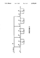
- FIG. 2 is a circuit diagram of two cells of a shift register 30 constructed in accordance with the invention.
- the shift register 30 includes pass gates 32, 36, 40 and 44, which are alternating NMOS and PMOS transistors with their gates tied to a single clock line 31.
- the pass gates are interconnected by inverters 34, 38, 42 and 46.
- the inverters hold the bit values passed by the previous associated pass gate, and the values are then passed through the next associated pass gate.
- Gates 32 and 36 and inverters 34 and 38 form a first cell
- gates 40 and 44 together with inverters 42 and 46 form a second cell.
- the shift register 30 is dynamic and thus the register must be shifted, that is, the bit values must be passed often from one cell to the next. Otherwise, a passed value, may, for example, deteriorate from a binary ONE, to a binary ZERO due to normal node leakage.
- the inverters 34, 38, 42 and 46 are level-sensing inverters, which compensate for signal levels which deteriorate as values are passed through the PMOS and NMOS gates. Specifically, when a PMOS transistor, for example, transistor 40, passes a binary ZERO, the transistor stops conducting prior to fully discharging the input to inverter 42. Inverter 42 thus receives a degraded binary ZERO signal. Similarly, when an NMOS transistor, for example, transistor 44, passes a binary ONE, it stops conducting prior to fully charging the input to inverter 46. Inverter 46 thus receives a degraded binary ONE signal. The PMOS transistor does not, however, adversely affect the voltage level of a binary ONE and the NMOS transistor does not adversely affect the voltage level of a binary ZERO. Accordingly, the associated inverters receive supply-level voltage levels for these logic states.
- the signal passing characteristics of the PMOS and NMOS transistors are attributable to the basic physics of the respective transistors. Accordingly, the inverters associated with the PMOS gates, namely, inverters 34 and 42, are designed to treat any voltage less than 20% of the supply voltage (VDD) as a logical ZERO, and the inverters associated with the NMOS gates, namely, inverters 38 and 46, are designed to treat any voltage greater than 80% of the supply voltage (VDD) as a logical ONE. The level-sensing inverters then produce full supply-level signals corresponding to the binary inverses of the received logical ZERO and ONE signals. These signals are next passed to the succeeding cells as binary ONES and binary ZEROS, respectively.
- pass gates 32 and 40 turn on and pass the values A 1 and A 2 into the first and second cells, respectively.
- Inverters 34 and 42 then invert the passed values to binary-valued inverse A 1 and inverse A 2 .
- the PMOS pass gates 32 and 40 shut off and the NMOS pass gates 36 and 44 turn on.
- the NMOS pass gates 36 and 44 then pass the inverse A 1 and inverse A 2 values to inverters 38 and 46, and the inverters 38 and 46 invert the passed values to binary-valued A 1 and A 2 , respectively.
- the clock signal again goes low it turns off the NMOS pass gates 36 and 44 and again turns on the PMOS pass gates 32 and 40.
- PMOS pass gate 40 passes the value A 1
- pass gate 32 passes a value A 0 (not shown).
- the shift register 30 requires only one clock signal, ⁇ , and thus, it does not require the clock generation or clock compensation circuitry discussed above with reference to FIG. 1. Accordingly, the shift register 30 requires fewer circuit components than does the shift register described above, and it is both smaller and less complex.
- the clock signal, ⁇ like the signals ⁇ c and ⁇ cc (FIG. 1), must have a fast edge-rate in order to avoid driving successive gates to conduct at the same time.
- providing a single fast-edge-rate clock signal to the register is much less of a problem than providing two such clock signals which must remain 180° out of phase, as described above.
- Shift register 30 does not include any refresh circuitry. Accordingly, any stored or held signals may deteriorate over time, due to normal node leakage. Thus register 30 is best suited for high-frequency applications, where the clock signal causes the pass gates to pass values at continuous, regular intervals.
- FIG. 3 is a diagram of a second embodiment of the invention.
- FIG. 3 depicts the shift register 30 of FIG. 2 with added refresh circuitry.
- the elements of FIG. 3 which are the same as the elements of FIG. 2 have been assigned the same reference numerals.
- the first cell consists of pass gates 32 and 36 and associated connecting and refresh circuitry, specifically inverters 34, 38 and 33, 37.
- PMOS pass gate 32 passes to level-sensing inverter 34 the bit value A 1 , which in this example is a binary ZERO.
- a 1 which in this example is a binary ZERO.
- PMOS pass gates shut off before fully discharging a binary ZERO input to a connected inverter.
- inverter 34 receives a degraded logical ZERO signal, which it inverts to a full supply-level binary ONE.
- the inverter 34 then supplies the inverted signal to the NMOS gate 36 and the feedback inverter 33.
- Feedback inverter 33 maintains or refreshes the signal at the input of inverter 34 as a binary ZERO by supplying to it the inverse of the received binary ONE.
- the feedback inverter 33 must have a relatively high impedance, that is, the inverter 33 must be relatively weak, to avoid writing the refresh value backward through PMOS gate 32 when the gate turns on to conduct forward.
- the added refresh circuitry which supplies feedback current to compensate for normal node leakage, enables the shift register to pass values at any frequency.
- the shift register is thus not limited to the virtually continuous operation of the dynamic register of FIG. 2.
- the pass gates require a finite amount of time to overcome the feedback current.
- this register may not be suitable for high frequency operation. Instead, it is best suited for medium to low-frequency applications.
- FIG. 4 illustrates a third embodiment of the current invention, which may be used when a high-speed shift register is required.
- FIG. 4 depicts the shift register of FIG. 3 with gated refresh circuitry. Again, elements which are the same in the previous two Figures have been assigned the same numerals.
- the shift register includes, in each refresh, or feedback, loop, a feedback gate such as feedback gate 35.
- the feedback gates are complements of the associated pass gate transistors.
- the feedback gate 35 associated with PMOS pass gate 32 is an NMOS transistor.
- the feedback gates operate to refresh passed bit values when the associated pass gates are shut off.
- These feedback gates in conjunction with the level-sensing inverters restore the held bit values to their proper levels as the values are passed to the next cells via the succeeding pass gates.
- the various inverter-feedback gate combinations restore only one of the two possible logic states to its full level, i.e., the NMOS gate combination fully restores only a logical ZERO and the PMOS gate combination fully restores only a logical ONE, this register may not be suitable for low-frequency operation.
- FIG. 5 illustrates one cell of a fourth embodiment of the current invention.
- This shift register is the same as the shift register shown in FIGS. 3 or 4, with added refresh circuitry.
- the first half of the shift register cell includes PMOS pass gate 32, inverters 34 and 49 which hold the passed value, or in the case of inverter 34 the inverse of the passed value, and feedback transistors 35 and 48, which refresh the bit values held in the cell.
- This configuration fully restores and maintains the voltage levels of both logical ONES and logical ZEROS, which enables the register to function even at low frequencies.
- pass gate 36 passes a binary ZERO to inverter 38
- the inverter presents to both transistor 50 and inverter 51 a logical ONE.
- transistor 50 turns on, and inverter 51 presents to both feedback transistors 39 and 50 a binary ZERO.
- Transistor 39 which turns on when the clock signal goes low supplies to inverter 38 a degraded logical ZERO.
- Transistor 50 supplies to inverter 38 a full-valued binary ZERO signal which fully restores the input signal.
- transistor 39 maintains the input of inverter 38 as a full-valued binary ONE.
- the refresh circuitry fully restores and maintains the input of inverter 38 at either a binary ZERO or a binary ONE, as appropriate.
- transistor 35 maintains the input of inverter 34 as a full binary ZERO when a ZERO is passed through pass gate 32 and, when a ONE is passed through pass gate 32, transistor 48 supplies to the input of inverter 34 a full-valued binary ONE.
- FIG. 6 depicts yet another embodiment of the invention.
- a shift register 50 includes in each cell a set of dual pass gates, namely, two NMOS gates 54 and 56, and two PMOS gates, 62 and 64, all driven by a single clock signal.
- the cells also include refresh inverters 57-58 and 65-66 and buffer inverters 59-60 and 67-68, which all may be of standard design.
- the inverters need not be level-sensing inverters because, as described below, held bit values are always refreshed to their full binary values.
- Each cell requires two complementary data input values, namely, A and inverse A.
- the inverters also operate together to restore nodes 55a and 55b to logical ONE and ZERO values, respectively.
- the cell is thus written with the logic state passed through gates 54 and 56. Moreover, by the time the pass gates 62 and 64 are ready to conduct, nodes 55a and 55b have been restored by the various inverters to the appropriate full logic levels.
- Shift register 50 requires complementary data values, instead of the complementary clock signals required by the prior art shift registers of FIG. 1. However, such data values are more easily supplied than are the two complementary clock signals. This is particularly true when the complementary data are present in the same or an adjacent cell. Further, complementary data values need not maintain an exact 180 degree phase shift relationship as is the case with prior art clock signals, as described above.
- the various embodiments of the current invention each use a single clock line--and thus avoid the need for special clock generation and clock compensation circuitry. Accordingly, the inventive shift registers are smaller, less complex and less expensive to fabricate than CMOS shift registers which use two clock signals.
Abstract
Description
Claims (4)
Priority Applications (1)
| Application Number | Priority Date | Filing Date | Title |
|---|---|---|---|
| US07/603,790 US5159616A (en) | 1990-10-25 | 1990-10-25 | CMOS shift register with complementary refresh pass gates and buffer |
Applications Claiming Priority (1)
| Application Number | Priority Date | Filing Date | Title |
|---|---|---|---|
| US07/603,790 US5159616A (en) | 1990-10-25 | 1990-10-25 | CMOS shift register with complementary refresh pass gates and buffer |
Publications (1)
| Publication Number | Publication Date |
|---|---|
| US5159616A true US5159616A (en) | 1992-10-27 |
Family
ID=24416922
Family Applications (1)
| Application Number | Title | Priority Date | Filing Date |
|---|---|---|---|
| US07/603,790 Expired - Lifetime US5159616A (en) | 1990-10-25 | 1990-10-25 | CMOS shift register with complementary refresh pass gates and buffer |
Country Status (1)
| Country | Link |
|---|---|
| US (1) | US5159616A (en) |
Cited By (8)
| Publication number | Priority date | Publication date | Assignee | Title |
|---|---|---|---|---|
| US5495513A (en) * | 1994-11-18 | 1996-02-27 | Advanced Micro Devices Inc. | Counter cell and counter circuit |
| US5497114A (en) * | 1993-12-22 | 1996-03-05 | Fujitsu Limited | Flip-flop circuit |
| US6018559A (en) * | 1995-12-19 | 2000-01-25 | Fujitsu Limited | Chain-connected shift register and programmable logic circuit whose logic function is changeable in real time |
| US6105106A (en) * | 1997-12-31 | 2000-08-15 | Micron Technology, Inc. | Computer system, memory device and shift register including a balanced switching circuit with series connected transfer gates which are selectively clocked for fast switching times |
| US6661727B2 (en) * | 1998-11-09 | 2003-12-09 | Broadcom Corporation | Dynamic register with low clock rate testing capability |
| US20130063404A1 (en) * | 2011-09-13 | 2013-03-14 | Abbas Jamshidi Roudbari | Driver Circuitry for Displays |
| CN107093463A (en) * | 2012-02-13 | 2017-08-25 | 中村维男 | Array, compound propulsion memory and the computer system of bit-level cell |
| CN112399111A (en) * | 2020-10-09 | 2021-02-23 | 电子科技大学中山学院 | Shift register and CMOS solid-state imaging sensor |
Citations (7)
| Publication number | Priority date | Publication date | Assignee | Title |
|---|---|---|---|---|
| US4084107A (en) * | 1975-12-19 | 1978-04-11 | Hitachi, Ltd. | Charge transfer device |
| US4250406A (en) * | 1978-12-21 | 1981-02-10 | Motorola, Inc. | Single clock CMOS logic circuit with selected threshold voltages |
| US4495629A (en) * | 1983-01-25 | 1985-01-22 | Storage Technology Partners | CMOS scannable latch |
| JPS6079599A (en) * | 1983-10-05 | 1985-05-07 | Nec Corp | Shift register circuit |
| DE3428393A1 (en) * | 1984-08-01 | 1986-02-13 | Siemens AG, 1000 Berlin und 8000 München | Clock-controlled bistable circuit |
| US4571504A (en) * | 1982-10-21 | 1986-02-18 | Tokyo Shibaura Denki Kabushiki Kaisha | Schmitt trigger circuit with selection circuit |
| US4705965A (en) * | 1984-10-01 | 1987-11-10 | U.S. Philips Corporation | Interference free D-type flip-flop |
-
1990
- 1990-10-25 US US07/603,790 patent/US5159616A/en not_active Expired - Lifetime
Patent Citations (7)
| Publication number | Priority date | Publication date | Assignee | Title |
|---|---|---|---|---|
| US4084107A (en) * | 1975-12-19 | 1978-04-11 | Hitachi, Ltd. | Charge transfer device |
| US4250406A (en) * | 1978-12-21 | 1981-02-10 | Motorola, Inc. | Single clock CMOS logic circuit with selected threshold voltages |
| US4571504A (en) * | 1982-10-21 | 1986-02-18 | Tokyo Shibaura Denki Kabushiki Kaisha | Schmitt trigger circuit with selection circuit |
| US4495629A (en) * | 1983-01-25 | 1985-01-22 | Storage Technology Partners | CMOS scannable latch |
| JPS6079599A (en) * | 1983-10-05 | 1985-05-07 | Nec Corp | Shift register circuit |
| DE3428393A1 (en) * | 1984-08-01 | 1986-02-13 | Siemens AG, 1000 Berlin und 8000 München | Clock-controlled bistable circuit |
| US4705965A (en) * | 1984-10-01 | 1987-11-10 | U.S. Philips Corporation | Interference free D-type flip-flop |
Non-Patent Citations (2)
| Title |
|---|
| IBM Tech. Disclosure Bul. vol. 12 No. 12 May 1970 "Complementary FET Dynamic Shift Register Using a Single Phase Line" by Gaensslen et al. |
| IBM Tech. Disclosure Bul. vol. 12 No. 12 May 1970 Complementary FET Dynamic Shift Register Using a Single Phase Line by Gaensslen et al. * |
Cited By (16)
| Publication number | Priority date | Publication date | Assignee | Title |
|---|---|---|---|---|
| US5497114A (en) * | 1993-12-22 | 1996-03-05 | Fujitsu Limited | Flip-flop circuit |
| US5495513A (en) * | 1994-11-18 | 1996-02-27 | Advanced Micro Devices Inc. | Counter cell and counter circuit |
| US6018559A (en) * | 1995-12-19 | 2000-01-25 | Fujitsu Limited | Chain-connected shift register and programmable logic circuit whose logic function is changeable in real time |
| US6404224B1 (en) | 1995-12-19 | 2002-06-11 | Fujitsu Limited | Chain-connected shift register and programmable logic circuit whose logic function is changeable in real time |
| US6105106A (en) * | 1997-12-31 | 2000-08-15 | Micron Technology, Inc. | Computer system, memory device and shift register including a balanced switching circuit with series connected transfer gates which are selectively clocked for fast switching times |
| US6516382B2 (en) | 1997-12-31 | 2003-02-04 | Micron Technology, Inc. | Memory device balanced switching circuit and method of controlling an array of transfer gates for fast switching times |
| US6522163B1 (en) | 1997-12-31 | 2003-02-18 | Micron Technology, Inc. | Apparatus and method for coupling a first node to a second node using switches which are selectively clocked for fast switching times |
| US6661727B2 (en) * | 1998-11-09 | 2003-12-09 | Broadcom Corporation | Dynamic register with low clock rate testing capability |
| US20130063404A1 (en) * | 2011-09-13 | 2013-03-14 | Abbas Jamshidi Roudbari | Driver Circuitry for Displays |
| CN107093463A (en) * | 2012-02-13 | 2017-08-25 | 中村维男 | Array, compound propulsion memory and the computer system of bit-level cell |
| EP3477645A1 (en) * | 2012-02-13 | 2019-05-01 | Tadao Nakamura | A marching memory, a bidirectional marching memory, a complex marching memory and a computer system, without the memory bottleneck |
| US10573359B2 (en) | 2012-02-13 | 2020-02-25 | Tadao Nakamura | Marching memory, a bidirectional marching memory, a complex marching memory and a computer system, without the memory bottleneck |
| CN107093463B (en) * | 2012-02-13 | 2021-01-01 | 中村维男 | Array of bit-level cells, compound advanced memory and computer system |
| US11164612B2 (en) | 2012-02-13 | 2021-11-02 | Tadao Nakamura | Marching memory, a bidirectional marching memory, a complex marching memory and a computer system, without the memory bottleneck |
| EP3982366A1 (en) * | 2012-02-13 | 2022-04-13 | Tadao Nakamura | A marching memory, a bidirectional marching memory, a complex marching memory and a computer system, without the memory bottleneck |
| CN112399111A (en) * | 2020-10-09 | 2021-02-23 | 电子科技大学中山学院 | Shift register and CMOS solid-state imaging sensor |
Similar Documents
| Publication | Publication Date | Title |
|---|---|---|
| US8077529B2 (en) | Circuit and method for outputting data in semiconductor memory apparatus | |
| US3989955A (en) | Logic circuit arrangements using insulated-gate field effect transistors | |
| KR102232554B1 (en) | Level shifter | |
| KR102310684B1 (en) | Level shifter enable | |
| KR20040103494A (en) | Register controlled delay locked loop with reduced delay locking time | |
| EP0408032B1 (en) | Data output control circuit for semiconductor storage device | |
| US5159616A (en) | CMOS shift register with complementary refresh pass gates and buffer | |
| US5408138A (en) | Flip flop circuit and method therefor | |
| US6111444A (en) | Edge triggered latch | |
| US5874845A (en) | Non-overlapping clock phase splitter | |
| US20080054944A1 (en) | Method and circuit for producing symmetrical output signals tolerant to input timing skew, output delay/slewrate-mismatch, and complementary device mismatch | |
| US5831463A (en) | MOS master-slave flip-flop with reduced number of pass gates | |
| US7528630B2 (en) | High speed flip-flop | |
| CN114567293B (en) | Latch, processor and computing device including latch | |
| KR100276563B1 (en) | Output buffer circuit | |
| JPH08138379A (en) | Nonsuperposed signal generation circuit of semiconductor memory device | |
| JP3573687B2 (en) | Data temporary storage | |
| JP3580483B2 (en) | Clock pulse generator, spatial light modulator and display | |
| JPH03231324A (en) | Dynamic barrel shifter | |
| US10936040B2 (en) | Semiconductor apparatus | |
| US20230386554A1 (en) | Power supply switching circuit and memory | |
| KR0154757B1 (en) | Semiconductor memory apparatus | |
| KR100358132B1 (en) | Circuit for discharging write bit line | |
| KR100189745B1 (en) | Equalization pulse generator of memory device | |
| CN110832775A (en) | Method and apparatus for a two-phase flip-flop with symmetric rise and fall times |
Legal Events
| Date | Code | Title | Description |
|---|---|---|---|
| AS | Assignment |
Owner name: DIGITAL EQUIPMENT CORPORATION, 111 POWDERMILL ROAD Free format text: ASSIGNMENT OF ASSIGNORS INTEREST.;ASSIGNORS:KASTNER, MICHAEL E.;RINNE, FLOYD P.;REEL/FRAME:005497/0451;SIGNING DATES FROM 19901023 TO 19901024 Owner name: DIGITAL EQUIPMENT CORPORATION, 111 POWDERMILL ROAD Free format text: ASSIGNMENT OF ASSIGNORS INTEREST.;ASSIGNOR:DOUGLAS, CHET R.;REEL/FRAME:005497/0446 Effective date: 19901024 |
|
| STCF | Information on status: patent grant |
Free format text: PATENTED CASE |
|
| FEPP | Fee payment procedure |
Free format text: PAYOR NUMBER ASSIGNED (ORIGINAL EVENT CODE: ASPN); ENTITY STATUS OF PATENT OWNER: LARGE ENTITY |
|
| FPAY | Fee payment |
Year of fee payment: 4 |
|
| FPAY | Fee payment |
Year of fee payment: 8 |
|
| AS | Assignment |
Owner name: COMPAQ INFORMATION TECHNOLOGIES GROUP, L.P., TEXAS Free format text: ASSIGNMENT OF ASSIGNORS INTEREST;ASSIGNORS:DIGITAL EQUIPMENT CORPORATION;COMPAQ COMPUTER CORPORATION;REEL/FRAME:012447/0903;SIGNING DATES FROM 19991209 TO 20010620 |
|
| AS | Assignment |
Owner name: HEWLETT-PACKARD DEVELOPMENT COMPANY, L.P., TEXAS Free format text: CHANGE OF NAME;ASSIGNOR:COMPAQ INFORMATION TECHNOLOGIES GROUP, LP;REEL/FRAME:015000/0305 Effective date: 20021001 |
|
| FPAY | Fee payment |
Year of fee payment: 12 |