US5148054A - High accuracy MOSFET-switched sampling circuit - Google Patents
High accuracy MOSFET-switched sampling circuit Download PDFInfo
- Publication number
- US5148054A US5148054A US07/741,549 US74154991A US5148054A US 5148054 A US5148054 A US 5148054A US 74154991 A US74154991 A US 74154991A US 5148054 A US5148054 A US 5148054A
- Authority
- US
- United States
- Prior art keywords
- mosfet
- input signal
- load
- isolating
- signal path
- Prior art date
- Legal status (The legal status is an assumption and is not a legal conclusion. Google has not performed a legal analysis and makes no representation as to the accuracy of the status listed.)
- Expired - Lifetime
Links
Images


Classifications
-
- H—ELECTRICITY
- H03—ELECTRONIC CIRCUITRY
- H03K—PULSE TECHNIQUE
- H03K17/00—Electronic switching or gating, i.e. not by contact-making and –breaking
- H03K17/51—Electronic switching or gating, i.e. not by contact-making and –breaking characterised by the components used
- H03K17/56—Electronic switching or gating, i.e. not by contact-making and –breaking characterised by the components used by the use, as active elements, of semiconductor devices
- H03K17/687—Electronic switching or gating, i.e. not by contact-making and –breaking characterised by the components used by the use, as active elements, of semiconductor devices the devices being field-effect transistors
- H03K17/693—Switching arrangements with several input- or output-terminals, e.g. multiplexers, distributors
-
- H—ELECTRICITY
- H03—ELECTRONIC CIRCUITRY
- H03K—PULSE TECHNIQUE
- H03K17/00—Electronic switching or gating, i.e. not by contact-making and –breaking
- H03K17/16—Modifications for eliminating interference voltages or currents
- H03K17/161—Modifications for eliminating interference voltages or currents in field-effect transistor switches
- H03K17/162—Modifications for eliminating interference voltages or currents in field-effect transistor switches without feedback from the output circuit to the control circuit
-
- H—ELECTRICITY
- H03—ELECTRONIC CIRCUITRY
- H03K—PULSE TECHNIQUE
- H03K5/00—Manipulating of pulses not covered by one of the other main groups of this subclass
- H03K5/22—Circuits having more than one input and one output for comparing pulses or pulse trains with each other according to input signal characteristics, e.g. slope, integral
- H03K5/24—Circuits having more than one input and one output for comparing pulses or pulse trains with each other according to input signal characteristics, e.g. slope, integral the characteristic being amplitude
- H03K5/2472—Circuits having more than one input and one output for comparing pulses or pulse trains with each other according to input signal characteristics, e.g. slope, integral the characteristic being amplitude using field effect transistors
- H03K5/249—Circuits having more than one input and one output for comparing pulses or pulse trains with each other according to input signal characteristics, e.g. slope, integral the characteristic being amplitude using field effect transistors using clock signals
Definitions
- the present invention is directed to the field of electrical interconnection circuits, more particularly, to a high-accuracy MOSFET switching circuit for alternatively sampling a DC reference signal and an AC input signal to a load, and more particularly, to such a circuit where the load includes a capacitive load.
- CMOS Complementary Metal-Oxide Semiconductor
- MOSFET Metal-Oxide-Semiconductor Field-Effect Transistors
- a MOSFET switching transistor is provided in the DC input signal path and another MOSFET switching transistor is provided in the AC input signal path.
- the MOSFET switching transistor in the DC input signal path is switched in non-overlapping phase opposition to the MOSFET switching transistor provided in the AC input signal path in such a way as to controllably switch the DC input signal and the AC input signal alternatively to the same load.
- undesirable currents are produced as the MOSFET switching transistor in the DC input signal path is switched from its "on” to its "off” condition.
- the currents induced by the parasitic capacitances and channel charge corrupt the DC input signal sampled onto the load, placing thereby a limit on the accuracy with which the AC signal is able to be alternatively sampled to the same load.
- charge feedthrough error To compensate the switching MOSFET in the DC input signal path for the unwanted currents, so-called "charge feedthrough error", it is known to provide a second, compensating MOSFET in the DC input signal path in series relation with the switching MOSFET thereof.
- the capacitance of the second, compensating MOSFET is selected to be equal to the parasitic capacitance exhibited by the gate to drain terminals of the MOSFET switching transistor in the DC input signal path to be compensated.
- the second, compensating MOSFET switched in phase opposition to the MOSFET switching transistor to be compensated in the DC input signal path, produces a current of a sign that cancels out the charge feedthrough error of the MOSFET switching transistor to be compensated in the DC input signal path.
- the unwanted current attributable to the charge of the channel and the unwanted current attributable to the parasitic capacitance of the gate to source terminals of the MOSFET switching transistor to be compensated are often either commensurate with or greater than the current attributable to the parasitic capacitance of the gate to drain parasitic capacitance thereof, which currents, uncompensated by the heretofore known charge feedthrough error compensation technique, corrupt the sampling of the DC input signal to the load and thereby limit the accuracy with which the AC input signal is able to be sampled to the same load.
- phase-opposed switching of the switching and compensating MOSFETS gives rise to the asymmetry that the compensating MOSFET produces its cancelling current before the switching MOSFET to be compensated is fully in its "off" condition.
- the compensating current produced by the compensating MOSFET instead of cancelling the charge feedthrough error by flowing to the load, rather flows out along the DC input signal path in such a way as to be dissipated by the input impedance thereof.
- phase delay may be interposed by which the switching and compensating MOSFETS are alternatively switched with an interval sufficient to enable the switching MOSFET to be fully turned to its "off” condition before the compensating MOSFET is turned to its "on” condition, the magnitude of the charge feedthrough error can nonetheless remain unsatisfactorily large.
- first means are disclosed in the DC input signal path for feeding no more than one half of the charge feedthrough error of the switching MOSFET to the load
- second means including an isolating MOSFET in the DC input signal path and cooperative with the first means are disclosed for electrically isolating the first means from the AC input signal path
- third means cooperative with the first and second means are disclosed for exactly compensating the charge feedthrough error introduced by the isolating MOSFET of the isolating means.
- the first means includes a dummy load in the DC input signal path that is electrically equivalent to and in electrically parallel relation with the load; the charge feedthrough error produced by the switching MOSFET in the DC input signal path is equally split between the dummy load and the load.
- the isolating MOSFET of the second means is provided in the DC input signal path in electrically serial relation between the dummy load and the load, and the second means includes means for switching the isolating MOSFET fully to the "off" condition thereof before the switching MOSFET in the AC input signal path is switched to the "on” condition thereof; the dummy load is thereby rendered transparent to the AC input signal path.
- the third means includes a compensating MOSFET having a preselected parasitic capacitance that is selected to exactly match the parasitic capacitance including channel charge of the isolating MOSFET of the second means.
- the compensating MOSFET exactly compensates both the currents attributable to the gate to drain parasitic capacitance as well as to the channel charge of the isolating MOSFET of the second means.
- the load and the dummy load can be selected to be electrically unequal, so as to shift more (or less) of the charge feedthrough error into the dummy load than to the load, and the parasitic capacitance of the compensating MOSFET can be selected to compensate the unwanted currents produced both by the switching MOSFET and by the isolating MOSFET.
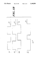
- FIG. 1A illustrates a schematic diagram and in the FIG. 1B thereof a timing diagram of a high-accuracy MOSFET-switched sampling circuit in accord with the present invention
- FIG. 2 is a schematic diagram of an exemplary auto-zeroed CMOS comparator embodying the high-accuracy MOSFET-switched sampling circuit in accord with the present invention.
- the high-accuracy MOSFET-switched sampling circuit 10 includes a DC input circuit path defined between an input terminal 12 marked “DC input” and an output terminal 14 marked “sampled output", and an AC input signal path defined between an input terminal 16 marked “AC input” and the output terminal 14.
- the voltage available at the output terminal 14 is the same voltage as that produced on a load capacitor 18 marked "Cl”.
- a first MOSFET switching transistor generally designated 20 is provided in serial relation along the DC input signal path.
- the first MOSFET switching transistor 20 is switched between its “on” and its “off” conditions under control of a clock marked “clk1" applied to a terminal 22 that is electrically connected in series to the gate of the first MOSFET switching transistor 20.
- a second MOSFET isolating transistor generally designated 24 is connected with its source in series with the drain of the first MOSFET switching transistor 20 and with its drain electrically connected in series to the output terminal 14.
- the second MOSFET isolating transistor 24 is switched between its "on” and its “off” conditions under control of a clock signal marked "clk2" applied to its gate terminal 26.
- a third MOSFET compensating transistor generally designated 28 is serially coupled in the DC input signal path between the drain of the second MOSFET isolating transistor 24 and the output terminal 14.
- the source and drain of the third MOSFET compensating transistor 28 are electrically shorted together.
- a clock marked “clk2B” is applied to the gate terminal 30 of the third MOSFET compensating transistor 28 to cause it to controllably assume its "on” and its “off” conditions.
- a dummy capacitor 32 marked “C dummy” is electrically connected in parallel to the load 18 in the DC input signal path between the drain of the switching MOSFET 20 and the source of the isolating MOSFET 24.
- a fourth MOSFET sampling transistor generally designated 34 is electrically connected in series in the AC input signal path with its source terminal connected to the AC input terminal 16 and with its drain electrically connected to the sampled output terminal 14.
- a clock marked “clk3" is connected to gate terminal 36 of the fourth MOSFET sampling transistor 34 to control its "on” and “off” conditions.
- the capacitors 18, 32 are selected to have an equal value of capacitance.
- the equivalent capacitance exhibited by the electrically-shorted source and drain terminals of the third MOSFET compensating transistor 28 is selected to match the gate to drain capacitance of the second MOSFET isolating transistor 24.
- Cp represents the magnitude of the gate to drain parasitic (offset) capacitance of the second MOSFET isolating transistor 24
- fabricating the third MOSFET compensating transistor 28 to have a gate to source parasitic capacitance of "Cp/2” and a gate to drain parasitic capacitance of "Cp/2” as by scaling the geometry of the junctions of the third MOSFET compensating transistor by the reciprocal factor of two, the equivalent capacitance "Cp" is seen across the shorted source to drain terminals thereof and one half the channel charge of the second MOSFET isolating is exhibited thereby.
- numeral 38 generally designates four timing clock signals designated "ph1", “ph2", “ph2B” and “ph3” that correspond respectively to the clock signals "clk1", “clk2”, “clk2B” and “clk3” of FIG. 1A, the first MOSFET switching transistor 20 and the second MOSFET isolating transistor 24 are cyclically caused to be in their “on” conditions substantially simultaneously as shown by the phase “1” and phase "2" clock signals 40, 42 respectively.
- the reference DC input voltage applied to the terminal 12 is electrically coupled to the loads 18, 32 cycle-to-cycle.
- the voltage on the dummy capacitor 32 tends to stabilize at and around the value of the voltage of the reference DC input signal. Subsequent sampling of the reference DC input voltage thereby will be read onto the load capacitor 18 as if the dummy capacitor 32 were electrically transparent to the DC input signal along the DC input signal path.
- the trailing edge of the phase "2" clock 42 trails the trailing edge of the phase "1" clock 40 so that the isolating MOSFET 24 remains in its “on” condition while the switching MOSFET 20 is caused to assume its "off” condition.
- Charge feedthrough error produced by the switching MOSFET 20 in the forward direction along the DC input signal path thereby substantially equally splits between the capacitors 18 and 32.
- the switching MOSFET 20 is in its "off" condition.
- the charge feedthrough error of the isolating MOSFET 24 as it is switched to its "off" condition cyclically, composed of unwanted currents attributable to both parasitic gate to source and gate to drain capacitance as well as to source to drain channel charge, is fed forward along the DC input signal path to the load capacitor 18 and backward therealong to the dummy capacitor 32, in such manner that the charge feedthrough error splits substantially equally therebetween.
- phase "2B" clock signal 44 trails the trailing edge of the phase "2" clock signal 42 cycle-to-cycle by an interval sufficient to insure that the isolating MOSFET 24 is completely in its "off” condition before the compensating MOSFET 28 is caused to assume its "on” condition.
- the compensating MOSFET 28 produces a current equal but opposite to the unwanted currents produced by the isolating MOSFET 24, including currents attributable to both parasitic gate to drain capacitance and to parasitic source to drain capacitance as well as to channel charge, that exactly compensate the load 18 for the effect of the unwanted current feed forward thereto as produced by the isolating MOSFET 24 assuming its "off” condition cycle-to-cycle.
- the third MOSFET compensating transistor is selected to produce a compensating current equal in magnitude to the charge feedthrough error that the second MOSFET isolating transistor induces in the load 18, namely, a compensating current equal in magnitude to the unwanted currents attributable to one half the channel charge and attributable to the gate to drain parasitic capacitance thereof.
- the voltage caused to be sampled at the load capacitor 18 from the voltage applied to the DC input terminal 12 is at least more accurate by a factor of two than for the heretofore known charge feedthrough error compensation technique.
- the leading edge of the phase "3" clock trails the leading edge of the phase “2B” clock signal 44 and the trailing edge thereof leads the leading edge of the phase "1" clock signal 40, so that the AC signal applied to the AC input terminal 16 is electrically connected to the sample output terminal 14 if and only if the isolating MOSFET 24 is already well into its "off” condition.
- the input analog signal applied to the terminal 16 thereby sees only the load capacitor 18 cycle-to-cycle, in a manner that is transparent to the dummy load 32.
- FIG. 2 generally designated at 50 is a schematic diagram illustrating an auto-zeroed CMOS comparator embodying the high-accuracy MOSFET-switched sampling circuit in accord with the present invention.
- an auto-zeroed CMOS comparator 50 is illustrated, it will be appreciated that the present invention has a wide range of application and is not limited to the exemplary auto-zeroed CMOS comparator 50 of the FIG. 2 embodiment of the present invention.
- the auto-zeroed CMOS comparator 50 includes a first switching MOSFET 52 in the DC input signal path that is connected to a terminal 54 at which a DC reference signal marked “ref" is applied, and a second switching MOSFET 56 in the AC input signal path connected with its source to a terminal 58 marked “input” at which an AC input signal is applied.
- An isolating MOSFET 60 is connected in the DC input signal path with its source serially connected to the drain of the switching MOSFET 52, and a compensating MOSFET 62, the source and the drain terminals of which are short-circuited as described above in connection with the description of the FIG. 1A embodiment, is connected in the DC input signal path to the drain of the isolating MOSFET 60.
- the first switching MOSFET 52, the isolating MOSFET 60 and the compensating MOSFET 62 in the DC input signal path are respectively switched between their "on” and their “off” conditions by a phase “1" clocking signal marked “PH1” applied to a terminal 64 of the MOSFET 52, by a phase “2" clocking signal marked “PH2” applied to the gate terminal 66 of the MOSFET 60 and by a phase “2B” clocking signal marked “PH2B” applied to the gate terminal 68 of the MOSFET 62 cycle-to-cycle.
- the second switching transistor 56 in the AC input signal path is switched between its “on” and its “off” conditions by a phase “3” clocking signal marked “PH3” applied to the gate terminal 70 of the MOSFET 56.
- the phase “1” , phase “2” , phase “2B” and phase “3” clocking signals are the same in relative phase as the correspondingly marked waveforms described above in connection with the description of FIG. 1B.
- the load seen by the AC input signal is constituted by a capacitor 72 marked “Cl” in series with a bank of active MOSFETS generally designated 74 that are coupled in a well-known manner to provide an inverter.
- the identical active load including a bank of dummy MOSFETS generally designated 76 and a dummy capacitor 78 marked "C dummy" is connected in the DC input signal path in electrically parallel relation with the load having the bank of MOSFETS 74 and load capacitor 72.
- the capacitance of the capacitor 78 is selected to be equal to the capacitance of the capacitor 72, and corresponding MOSFETS of the bank of MOSFETS that constitute the analog inverter 76 are matched to the MOSFETS of the bank of MOSFETS that constitute the analog inverter 74.
- the MOSFETS marked “MN1" and “MN2" of the analog inverter's 74, 76 have their gate terminals connected to the phase "2" clocking signal.
- the phase "2" clocking signals control the "on” and “off” conditions of the MOSFETS MN1, MN2 of the analog inverters 74, 76 in such a way that when the MOSFETS MN1, MN2 thereof are in their "on” condition, the corresponding analog inverters 74, 76 are held at their metastable point.
- the input AC signal is capacitively coupled to the analog inverter 74 by the phase "3" clocking signal at times corresponding to the MOSFET MN1 of the analog inverter 74 being switched to its "off” condition by the phase "2" clocking signal.
- the analog inverter 74 moves above and below its logic threshold defined by its metastable point.
- the output thereof gives the logical comparison of the relative magnitudes of the reference DC input signal and the magnitude of the input AC signal as it is driven either above or below the metastable point that defines its logical threshold.
- the second gain stage 80 Downstream of the analog inverter 74 is a second gain stage generally designated 80.
- the second gain stage 80 is constructed of a bank of MOSFETS that function as an analog inverter.
- the output of the second gain stage is applied via a terminal 82 marked "out 2" to a latch, not shown.
- the switching MOSFET 52 and the isolating MOSFET 60 are cyclically held in their "on” conditions and the DC input signal applied to the terminal 54 is coupled along the DC input signal path in parallel to the active loads 72, 74; 76, 78.
- the phase "3" clocking signal keeps the second switching MOSFET 56 in its “off” condition whenever the phase "1” and phase 2 clocking signals hold the MOSFETS 52, 60 in their “on” conditions.
- phase “1” and the phase “2" clocking signals are so phased that the trailing edge of the phase “1” clocking signal leads the trailing edge of the phase “2” clocking signal by a time interval selected to enable the first switching MOSFET 52 to be completely in its “off” condition before the isolating MOSFET 60 is in its “off” condition.
- the charge feedthrough error in the forward direction produced by the parasitic capacitance of the first switching MOSFET 52 thereby is equally split between the active loads 72, 74; 76, 78 and is stored on the capacitors 72 and 78 thereof.
- phase "2" clocking signal and the phase “2B” clocking signal are in phase opposition, and the trailing edge of the phase “2" clocking signal is selected to lead the leading edge of the phase “2B” clocking signal by a time interval sufficient to insure that the isolating MOSFET 60 is completely in its “off” condition before the compensating MOSFET 62 is in its “on” condition.
- the charge feedthrough error produced by the isolating MOSFET 60 as it is switched to its "off” condition splits equally between the active loads 72, 74; 76, 78 and is stored in equal parts on the capacitors 72, 78 thereof.
- the unwanted currents associated with the gate to source parasitic capacitance and substantially one half of the current associated with the channel charge are stored in the dummy capacitor 78 and the unwanted currents associated with the gate to drain parasitic capacitance and substantially the other half of the currents associated with the channel charge are stored on the capacitor 72.
- the compensating MOSFET 62 which in the preferred embodiment is selected to have a parasitic capacitance and channel charge equal to that of the gate to drain parasitic capacitance and substantially one-half the channel charge of the isolating MOSFET 60, thereby completely cancels the error on the capacitor 72 produced by the isolating MOSFET's 60 unwanted current as it is turned to its "off" condition by the phase "2" clocking signal.
- phase " 3" clocking signal trails the trailing edge of the phase "2" clocking signal to insure that the input AC signal is only seen by the load 72, 74, but not by the dummy load 76, 78.
- the phase "2" clocking signal of the isolating MOSFET 60 keeps the isolating MOSFET 60 in its “off” condition at times when the phase "3" clocking signal turns the sampling MOSFET 56 to its “on” condition and thereby isolates the AC input signal path from the dummy load 76, 78.
- the dummy capacitor 78 Once the dummy capacitor 78 is initially charged to the reference voltage applied thereto along the DC input signal path, it does not require any further significant charging current. This produces the effect that the DC input signal only sees the capacitor 72, effectively making the dummy capacitor 78 transparent to the DC input signal.
- the isolating MOSFET 60 isolates the AC input signal from the dummy capacitor 78 of the dummy active load 76. The AC input signal thereby only sees the load 72, 74, but is transparent to the load 76, 78, and no penalty is paid by the presence of the dummy load 76, 78.
Landscapes
- Physics & Mathematics (AREA)
- Nonlinear Science (AREA)
- Electronic Switches (AREA)
Abstract
Description
Claims (20)
Priority Applications (1)
| Application Number | Priority Date | Filing Date | Title |
|---|---|---|---|
| US07/741,549 US5148054A (en) | 1991-08-07 | 1991-08-07 | High accuracy MOSFET-switched sampling circuit |
Applications Claiming Priority (1)
| Application Number | Priority Date | Filing Date | Title |
|---|---|---|---|
| US07/741,549 US5148054A (en) | 1991-08-07 | 1991-08-07 | High accuracy MOSFET-switched sampling circuit |
Publications (1)
| Publication Number | Publication Date |
|---|---|
| US5148054A true US5148054A (en) | 1992-09-15 |
Family
ID=24981165
Family Applications (1)
| Application Number | Title | Priority Date | Filing Date |
|---|---|---|---|
| US07/741,549 Expired - Lifetime US5148054A (en) | 1991-08-07 | 1991-08-07 | High accuracy MOSFET-switched sampling circuit |
Country Status (1)
| Country | Link |
|---|---|
| US (1) | US5148054A (en) |
Cited By (15)
| Publication number | Priority date | Publication date | Assignee | Title |
|---|---|---|---|---|
| US5338988A (en) * | 1992-10-21 | 1994-08-16 | Motorola, Inc. | Voltage converting circuit with low consumption driver |
| US5381053A (en) * | 1992-09-29 | 1995-01-10 | Nec Corporation | Voltage comparator circuit capable of avoiding erroneous operation |
| US5414311A (en) * | 1993-09-14 | 1995-05-09 | Carnegie Mellon University | Sample and hold circuit and finite impulse response filter constructed therefrom |
| US5457415A (en) * | 1992-10-30 | 1995-10-10 | International Business Machines Corporation | Charge metering sampling circuit and use thereof in TFT/LCD |
| US5534815A (en) * | 1994-07-29 | 1996-07-09 | Hewlett-Packard Company | Switching circuit for signal sampling with reduced residual charge effects |
| US5572153A (en) * | 1995-03-03 | 1996-11-05 | Lucent Technologies Inc. | Low offset comparators based on current copiers |
| US5760616A (en) * | 1995-09-05 | 1998-06-02 | Lucent Technologies, Inc. | Current copiers with improved accuracy |
| EP0917289A3 (en) * | 1997-11-17 | 2000-12-27 | STMicroelectronics GmbH | Integrated circuit with switched capacitor |
| US6229354B1 (en) * | 1998-12-22 | 2001-05-08 | Nokia Mobile Phones Ltd. | Method and circuit arrangement for signal processing |
| US6407592B2 (en) * | 2000-03-29 | 2002-06-18 | Kawasaki Microelectronics, Inc. | Sample-and-hold circuit |
| US20030098722A1 (en) * | 2000-12-28 | 2003-05-29 | Jensen Richard S. | Low charge-dump transistor switch |
| US20030132784A1 (en) * | 2001-11-29 | 2003-07-17 | Alcatel | Sampling phase detector |
| US6696884B1 (en) * | 2002-12-10 | 2004-02-24 | National Semiconductor Corporation | Method and apparatus to achieve long time constants with a small MOS gate capacitor |
| EP3806334A1 (en) * | 2019-10-07 | 2021-04-14 | IniVation AG | Switched capacitor circuit |
| US11038501B2 (en) * | 2019-04-29 | 2021-06-15 | Db Hitek Co., Ltd. | Transistor circuit and electronic circuit having same |
Citations (7)
| Publication number | Priority date | Publication date | Assignee | Title |
|---|---|---|---|---|
| US3586880A (en) * | 1969-08-11 | 1971-06-22 | Astrodata Inc | Isolation and compensation of sample and hold circuits |
| US4075509A (en) * | 1976-10-12 | 1978-02-21 | National Semiconductor Corporation | Cmos comparator circuit and method of manufacture |
| US4323796A (en) * | 1980-01-30 | 1982-04-06 | Motorola, Inc. | Low transient feedthru FET sample and hold gate |
| US4461965A (en) * | 1980-08-18 | 1984-07-24 | National Semiconductor Corporation | High speed CMOS sense amplifier |
| JPS6086908A (en) * | 1983-10-19 | 1985-05-16 | Hitachi Ltd | comparator |
| US4691125A (en) * | 1986-10-03 | 1987-09-01 | Motorola, Inc. | One hundred percent duty cycle sample-and-hold circuit |
| US4922130A (en) * | 1988-05-26 | 1990-05-01 | Hewlett-Packard Company | High performance track/hold for a digital multimeter |
-
1991
- 1991-08-07 US US07/741,549 patent/US5148054A/en not_active Expired - Lifetime
Patent Citations (7)
| Publication number | Priority date | Publication date | Assignee | Title |
|---|---|---|---|---|
| US3586880A (en) * | 1969-08-11 | 1971-06-22 | Astrodata Inc | Isolation and compensation of sample and hold circuits |
| US4075509A (en) * | 1976-10-12 | 1978-02-21 | National Semiconductor Corporation | Cmos comparator circuit and method of manufacture |
| US4323796A (en) * | 1980-01-30 | 1982-04-06 | Motorola, Inc. | Low transient feedthru FET sample and hold gate |
| US4461965A (en) * | 1980-08-18 | 1984-07-24 | National Semiconductor Corporation | High speed CMOS sense amplifier |
| JPS6086908A (en) * | 1983-10-19 | 1985-05-16 | Hitachi Ltd | comparator |
| US4691125A (en) * | 1986-10-03 | 1987-09-01 | Motorola, Inc. | One hundred percent duty cycle sample-and-hold circuit |
| US4922130A (en) * | 1988-05-26 | 1990-05-01 | Hewlett-Packard Company | High performance track/hold for a digital multimeter |
Non-Patent Citations (4)
| Title |
|---|
| C. Eichenberger and W. Guggenb hl, Dummy Transistor Compensation of Analog MOS Switches , IEEE Journal of Solid State Circuits vol. 24, No. 4 pp. 1143 1145 (Aug. 1989). * |
| C. Eichenberger and W. Guggenbuhl, "Dummy Transistor Compensation of Analog MOS Switches", IEEE Journal of Solid State Circuits vol. 24, No. 4 pp. 1143-1145 (Aug. 1989). |
| R. E. Suarez and P. R. Gray, "All-MOS Charge Redistribution Analog-to-Digital Conversion Techniques-Part II", IEEE Journal of Solid State Circuits vol. SC-10, pp. 379-385, (Dec. 1975). |
| R. E. Suarez and P. R. Gray, All MOS Charge Redistribution Analog to Digital Conversion Techniques Part II , IEEE Journal of Solid State Circuits vol. SC 10, pp. 379 385, (Dec. 1975). * |
Cited By (24)
| Publication number | Priority date | Publication date | Assignee | Title |
|---|---|---|---|---|
| US5381053A (en) * | 1992-09-29 | 1995-01-10 | Nec Corporation | Voltage comparator circuit capable of avoiding erroneous operation |
| US5338988A (en) * | 1992-10-21 | 1994-08-16 | Motorola, Inc. | Voltage converting circuit with low consumption driver |
| US5457415A (en) * | 1992-10-30 | 1995-10-10 | International Business Machines Corporation | Charge metering sampling circuit and use thereof in TFT/LCD |
| US5414311A (en) * | 1993-09-14 | 1995-05-09 | Carnegie Mellon University | Sample and hold circuit and finite impulse response filter constructed therefrom |
| US5534815A (en) * | 1994-07-29 | 1996-07-09 | Hewlett-Packard Company | Switching circuit for signal sampling with reduced residual charge effects |
| US5572153A (en) * | 1995-03-03 | 1996-11-05 | Lucent Technologies Inc. | Low offset comparators based on current copiers |
| US5760616A (en) * | 1995-09-05 | 1998-06-02 | Lucent Technologies, Inc. | Current copiers with improved accuracy |
| EP0917289A3 (en) * | 1997-11-17 | 2000-12-27 | STMicroelectronics GmbH | Integrated circuit with switched capacitor |
| US6229354B1 (en) * | 1998-12-22 | 2001-05-08 | Nokia Mobile Phones Ltd. | Method and circuit arrangement for signal processing |
| US6476647B2 (en) | 1998-12-22 | 2002-11-05 | Nokia Mobile Phones Ltd. | Method and circuit arrangement for signal processing |
| US6407592B2 (en) * | 2000-03-29 | 2002-06-18 | Kawasaki Microelectronics, Inc. | Sample-and-hold circuit |
| US20030098722A1 (en) * | 2000-12-28 | 2003-05-29 | Jensen Richard S. | Low charge-dump transistor switch |
| US6781434B2 (en) * | 2000-12-28 | 2004-08-24 | Intel Corporation | Low charge-dump transistor switch |
| US20030132784A1 (en) * | 2001-11-29 | 2003-07-17 | Alcatel | Sampling phase detector |
| US6696884B1 (en) * | 2002-12-10 | 2004-02-24 | National Semiconductor Corporation | Method and apparatus to achieve long time constants with a small MOS gate capacitor |
| US11038501B2 (en) * | 2019-04-29 | 2021-06-15 | Db Hitek Co., Ltd. | Transistor circuit and electronic circuit having same |
| EP3806334A1 (en) * | 2019-10-07 | 2021-04-14 | IniVation AG | Switched capacitor circuit |
| WO2021069278A1 (en) * | 2019-10-07 | 2021-04-15 | Inivation Ag | Switched capacitor circuit |
| KR20220048036A (en) * | 2019-10-07 | 2022-04-19 | 이니베이션 아게 | switched capacitor circuit |
| CN114556785A (en) * | 2019-10-07 | 2022-05-27 | 英尼维顺股份有限公司 | Switched capacitor circuit |
| JP2022552212A (en) * | 2019-10-07 | 2022-12-15 | イニベーション・アー・ゲー | switched capacitor circuit |
| JP7461673B2 (en) | 2019-10-07 | 2024-04-04 | イニベーション・アー・ゲー | Switched Capacitor Circuit |
| US12206429B2 (en) | 2019-10-07 | 2025-01-21 | Inivation Ag | Switched capacitor circuit |
| CN114556785B (en) * | 2019-10-07 | 2026-02-06 | 宁波时视科技有限公司 | Switched capacitor circuit |
Similar Documents
| Publication | Publication Date | Title |
|---|---|---|
| US5148054A (en) | High accuracy MOSFET-switched sampling circuit | |
| KR100590464B1 (en) | Sampling switch | |
| KR960012801B1 (en) | Ripple-free phase detector using two sample-and-hold circuit | |
| US4988902A (en) | Semiconductor transmission gate with capacitance compensation | |
| FI98016C (en) | -Channel transistor comparison circuit | |
| US6046612A (en) | Self-resetting comparator circuit and method | |
| KR920000839B1 (en) | A flash a/d converter | |
| EP3203480A1 (en) | Voltage sampling switch and method therefor | |
| US6215348B1 (en) | Bootstrapped low-voltage switch | |
| US10295572B1 (en) | Voltage sampling switch | |
| EP0509585A1 (en) | Clocked comparator with offset-voltage compensation | |
| JP2685050B2 (en) | Comparator circuit | |
| JP2591066B2 (en) | Analog switch circuit | |
| US4328434A (en) | Comparator circuit with offset correction | |
| US5165058A (en) | Voltage comparator with sample hold circuit | |
| US5534815A (en) | Switching circuit for signal sampling with reduced residual charge effects | |
| DE69615910T2 (en) | Switched capacitor interface circuit | |
| US8232904B2 (en) | Folding analog-to-digital converter | |
| US5329247A (en) | Switchable MOS current mirror | |
| US4162539A (en) | Read-out circuit for digital storage elements | |
| US5570048A (en) | Sample-and-hold circuit with reduced clock feedthrough | |
| US5717623A (en) | Analog current memory having resistance to reduce current transport error | |
| Sonkusale et al. | A low distortion MOS sampling circuit | |
| EP0594242B1 (en) | Sample-and-hold circuit with reduced clock feedthrough | |
| US20030094981A1 (en) | Chopper type comparator |
Legal Events
| Date | Code | Title | Description |
|---|---|---|---|
| AS | Assignment |
Owner name: MICRO NETWORKS, DIVISION OF UNITRODE CORPORATION Free format text: ASSIGNMENT OF ASSIGNORS INTEREST.;ASSIGNOR:DEMLER, MICHAEL J.;REEL/FRAME:005806/0972 Effective date: 19910801 |
|
| AS | Assignment |
Owner name: UNITRODE CORPORATION A CORP. OF MD Free format text: CHANGE OF ADDRESS OF ASSIGNEE.;ASSIGNOR:UNITRODE CORPORATION, A MD CORP. 5 FORBES RD., LEXINGTON, MA 02173;REEL/FRAME:005919/0244 Effective date: 19911114 |
|
| STCF | Information on status: patent grant |
Free format text: PATENTED CASE |
|
| AS | Assignment |
Owner name: CIT GROUP/CREDIT FINANCE, INC., THE 332 SOUTH M Free format text: SECURITY INTEREST;ASSIGNOR:MICRO NETWORKS CORPORATION;REEL/FRAME:007203/0199 Effective date: 19941012 |
|
| FEPP | Fee payment procedure |
Free format text: PAYOR NUMBER ASSIGNED (ORIGINAL EVENT CODE: ASPN); ENTITY STATUS OF PATENT OWNER: LARGE ENTITY Free format text: PAT HOLDER CLAIMS SMALL ENTITY STATUS - SMALL BUSINESS (ORIGINAL EVENT CODE: SM02); ENTITY STATUS OF PATENT OWNER: LARGE ENTITY |
|
| FPAY | Fee payment |
Year of fee payment: 4 |
|
| REMI | Maintenance fee reminder mailed | ||
| FPAY | Fee payment |
Year of fee payment: 8 |
|
| SULP | Surcharge for late payment | ||
| AS | Assignment |
Owner name: MNC WORCESTER CORPORATION, MASSACHUSETTS Free format text: CHANGE OF NAME;ASSIGNOR:MICRO NETWORKS CORPORATION;REEL/FRAME:012083/0865 Effective date: 19990713 |
|
| FEPP | Fee payment procedure |
Free format text: PAT HOLDER NO LONGER CLAIMS SMALL ENTITY STATUS, ENTITY STATUS SET TO UNDISCOUNTED (ORIGINAL EVENT CODE: STOL); ENTITY STATUS OF PATENT OWNER: LARGE ENTITY |
|
| REFU | Refund |
Free format text: REFUND - PAYMENT OF MAINTENANCE FEE, 12TH YR, SMALL ENTITY (ORIGINAL EVENT CODE: R2553); ENTITY STATUS OF PATENT OWNER: LARGE ENTITY |
|
| FPAY | Fee payment |
Year of fee payment: 12 |
|
| AS | Assignment |
Owner name: ICS TECHNOLOGIES, INC., DELAWARE Free format text: ASSIGNMENT OF ASSIGNORS INTEREST;ASSIGNOR:MNC WORCESTER CORPORATION.;REEL/FRAME:015242/0792 Effective date: 20040206 |
|
| AS | Assignment |
Owner name: MICRO NETWORKS CORPORATION, MASSACHUSETTS Free format text: RELEASE OF SECURITY INTEREST;ASSIGNOR:CIT GROUP/CREDIT FINANCE, INC.;REEL/FRAME:015878/0384 Effective date: 20040730 |
|
| AS | Assignment |
Owner name: INTEGRATED DEVICE TECHNOLOGY, INC., CALIFORNIA Free format text: ASSIGNMENT OF ASSIGNORS INTEREST;ASSIGNOR:ICS TECHNOLOGIES, INC.;REEL/FRAME:018279/0284 Effective date: 20060920 |
|
| AS | Assignment |
Owner name: SPECTRUM MICROWAVE, INC., PENNSYLVANIA Free format text: ASSIGNMENT OF ASSIGNORS INTEREST;ASSIGNOR:INTEGRATED DEVICE TECHNOLOGY, INC.;REEL/FRAME:023699/0811 Effective date: 20091130 |