US5130262A - Internal current limit and overvoltage protection method - Google Patents
Internal current limit and overvoltage protection method Download PDFInfo
- Publication number
- US5130262A US5130262A US07/704,683 US70468391A US5130262A US 5130262 A US5130262 A US 5130262A US 70468391 A US70468391 A US 70468391A US 5130262 A US5130262 A US 5130262A
- Authority
- US
- United States
- Prior art keywords
- region
- junction
- predetermined
- voltage
- current
- Prior art date
- Legal status (The legal status is an assumption and is not a legal conclusion. Google has not performed a legal analysis and makes no representation as to the accuracy of the status listed.)
- Expired - Lifetime
Links
- 238000000034 method Methods 0.000 title claims abstract description 20
- 239000004065 semiconductor Substances 0.000 claims abstract description 28
- 239000002019 doping agent Substances 0.000 claims abstract description 27
- 230000000903 blocking effect Effects 0.000 claims abstract description 11
- 239000000758 substrate Substances 0.000 claims description 11
- 239000000463 material Substances 0.000 claims description 9
- 239000003989 dielectric material Substances 0.000 claims 2
- 230000015572 biosynthetic process Effects 0.000 description 3
- XUIMIQQOPSSXEZ-UHFFFAOYSA-N Silicon Chemical compound [Si] XUIMIQQOPSSXEZ-UHFFFAOYSA-N 0.000 description 2
- 230000006378 damage Effects 0.000 description 2
- 238000012986 modification Methods 0.000 description 2
- 230000004048 modification Effects 0.000 description 2
- 230000001681 protective effect Effects 0.000 description 2
- 238000013459 approach Methods 0.000 description 1
- 230000001419 dependent effect Effects 0.000 description 1
- 238000010348 incorporation Methods 0.000 description 1
- 238000004519 manufacturing process Methods 0.000 description 1
- 229910052710 silicon Inorganic materials 0.000 description 1
- 239000010703 silicon Substances 0.000 description 1
Images

Classifications
-
- H—ELECTRICITY
- H01—ELECTRIC ELEMENTS
- H01L—SEMICONDUCTOR DEVICES NOT COVERED BY CLASS H10
- H01L29/00—Semiconductor devices adapted for rectifying, amplifying, oscillating or switching, or capacitors or resistors with at least one potential-jump barrier or surface barrier, e.g. PN junction depletion layer or carrier concentration layer; Details of semiconductor bodies or of electrodes thereof ; Multistep manufacturing processes therefor
- H01L29/02—Semiconductor bodies ; Multistep manufacturing processes therefor
- H01L29/06—Semiconductor bodies ; Multistep manufacturing processes therefor characterised by their shape; characterised by the shapes, relative sizes, or dispositions of the semiconductor regions ; characterised by the concentration or distribution of impurities within semiconductor regions
- H01L29/10—Semiconductor bodies ; Multistep manufacturing processes therefor characterised by their shape; characterised by the shapes, relative sizes, or dispositions of the semiconductor regions ; characterised by the concentration or distribution of impurities within semiconductor regions with semiconductor regions connected to an electrode not carrying current to be rectified, amplified or switched and such electrode being part of a semiconductor device which comprises three or more electrodes
- H01L29/1004—Base region of bipolar transistors
- H01L29/1008—Base region of bipolar transistors of lateral transistors
-
- H—ELECTRICITY
- H01—ELECTRIC ELEMENTS
- H01L—SEMICONDUCTOR DEVICES NOT COVERED BY CLASS H10
- H01L29/00—Semiconductor devices adapted for rectifying, amplifying, oscillating or switching, or capacitors or resistors with at least one potential-jump barrier or surface barrier, e.g. PN junction depletion layer or carrier concentration layer; Details of semiconductor bodies or of electrodes thereof ; Multistep manufacturing processes therefor
- H01L29/02—Semiconductor bodies ; Multistep manufacturing processes therefor
- H01L29/36—Semiconductor bodies ; Multistep manufacturing processes therefor characterised by the concentration or distribution of impurities in the bulk material
-
- H—ELECTRICITY
- H01—ELECTRIC ELEMENTS
- H01L—SEMICONDUCTOR DEVICES NOT COVERED BY CLASS H10
- H01L29/00—Semiconductor devices adapted for rectifying, amplifying, oscillating or switching, or capacitors or resistors with at least one potential-jump barrier or surface barrier, e.g. PN junction depletion layer or carrier concentration layer; Details of semiconductor bodies or of electrodes thereof ; Multistep manufacturing processes therefor
- H01L29/66—Types of semiconductor device ; Multistep manufacturing processes therefor
- H01L29/68—Types of semiconductor device ; Multistep manufacturing processes therefor controllable by only the electric current supplied, or only the electric potential applied, to an electrode which does not carry the current to be rectified, amplified or switched
- H01L29/70—Bipolar devices
- H01L29/72—Transistor-type devices, i.e. able to continuously respond to applied control signals
- H01L29/73—Bipolar junction transistors
- H01L29/732—Vertical transistors
- H01L29/7322—Vertical transistors having emitter-base and base-collector junctions leaving at the same surface of the body, e.g. planar transistor
-
- H—ELECTRICITY
- H01—ELECTRIC ELEMENTS
- H01L—SEMICONDUCTOR DEVICES NOT COVERED BY CLASS H10
- H01L29/00—Semiconductor devices adapted for rectifying, amplifying, oscillating or switching, or capacitors or resistors with at least one potential-jump barrier or surface barrier, e.g. PN junction depletion layer or carrier concentration layer; Details of semiconductor bodies or of electrodes thereof ; Multistep manufacturing processes therefor
- H01L29/66—Types of semiconductor device ; Multistep manufacturing processes therefor
- H01L29/68—Types of semiconductor device ; Multistep manufacturing processes therefor controllable by only the electric current supplied, or only the electric potential applied, to an electrode which does not carry the current to be rectified, amplified or switched
- H01L29/70—Bipolar devices
- H01L29/72—Transistor-type devices, i.e. able to continuously respond to applied control signals
- H01L29/73—Bipolar junction transistors
- H01L29/735—Lateral transistors
-
- Y—GENERAL TAGGING OF NEW TECHNOLOGICAL DEVELOPMENTS; GENERAL TAGGING OF CROSS-SECTIONAL TECHNOLOGIES SPANNING OVER SEVERAL SECTIONS OF THE IPC; TECHNICAL SUBJECTS COVERED BY FORMER USPC CROSS-REFERENCE ART COLLECTIONS [XRACs] AND DIGESTS
- Y10—TECHNICAL SUBJECTS COVERED BY FORMER USPC
- Y10S—TECHNICAL SUBJECTS COVERED BY FORMER USPC CROSS-REFERENCE ART COLLECTIONS [XRACs] AND DIGESTS
- Y10S148/00—Metal treatment
- Y10S148/011—Bipolar transistors
Definitions
- This invention relates, in general, to semiconductor devices, and more particularly to a method of fabricating a semiconductor device having internal current limit and overvoltage protection.
- One prior art method of device protection includes the addition of internal or external zener diodes to clamp the emitter-base or collector-emitter junction voltage. When the voltage exceeds the zener voltage, the zener diodes turn on, thereby limiting current.
- An obvious problem with this method is that the number of zener diodes employed internally depends upon the voltage which the primary transistor is to be turned off. When a high voltage transistor is employed, an excessive number of zener diodes must also be employed. This dissipates power, increases cost, and increases the amount of chip area required.
- Another protective method includes the incorporation of emitter ballast resistors to improve the uniformity of current distribution in a device and increase the maximum limit of power dissipation. Although this is somewhat successful, it still requires the addition of external devices which require increased amounts of chip area.
- Another object of this invention is to provide a method of internally limiting current and providing overvoltage protection in a semiconductor device wherein the pinch-off voltage may be adjusted for a given device.
- Yet a further object of the present invention is to provide a method of internally limiting current and providing overvoltage protection that may be employed in conjunction with high voltage semiconductor devices.
- An even further object of the present invention is to provide a method of internally limiting current and providing overvoltage protection that does not dissipate power from a device.
- one embodiment in which, as a part thereof, includes providing a substrate having semiconductor material of a first conductivity type and predetermined dopant concentration therein. First and second field regions of a second conductivity type and predetermined dopant concentrations are then formed in the semiconductor material so that first and second junctions exist therein, the junctions being spaced apart a predetermined distance. A base region of the first conductivity type and of a predetermined dopant concentration is then formed in the semiconductor material between the first and second field regions followed by the formation of an emitter region of the second conductivity type within the base region.
- the predetermined dopant concentrations and distance are such that when a predetermined voltage is applied to the device, a depletion region from the first junction encounters a depletion region from the second junction, thereby pinching-off current.
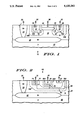
- FIGS. 1-4 are highly enlarged cross-sectional views of portions of semiconductor devices illustrating different embodiments of the present invention.
- FIGS. 1-4 are highly enlarged cross-sectional views of portions of semiconductor devices embodying the present invention.
- FIG. 1 illustrates a portion of a lateral bipolar device 10.
- device 10 is a PNP device, it should be understood that the present invention may also be employed in conjunction with an NPN device.
- device 10 comprises specific semiconductor materials, one of skill in the art will understand that many other well known semiconductor materials may be employed.
- the various distances and dopant concentrations given for device 10 are specifically for a device having a pinch-off voltage of 100 volts. As will be explained presently, the pinch-off voltage for a given device may be varied by adjusting the various dopant concentrations and distances.
- Device 10 includes a monosilicon substrate 12, having a P conductivity type.
- An epitaxial silicon layer 14, having an N conductivity type, is formed thereon.
- Epitaxial layer 14 has a dopant concentration of approximately 1.5 ⁇ 10 15 cm -3 .
- a buried layer 16, having an N + conductivity type is formed at the interface of substrate 12 and epitaxial layer 14. Buried layer 16 is contacted by N + region 18, which extends to the surface of epitaxial layer 14 and through which base contact is made at external base contact 20.
- a first field region 22 and a second field region 24 are formed in epitaxial layer 14.
- Field regions 22 and 24 both are of a P conductivity type, have a dopant concentration of approximately 5 ⁇ 1015 cm -3 and are approximately 9 microns apart. It should be understood that the dopant concentrations of first and second field regions 22 and 24 may differ although they do not in this embodiment.
- First and second P + collector contact regions 26 and 28, respectively, are formed in first and second field regions 22 and 24. External collector contact is made through first and second collector contact regions 26 and 28 by first and second external collector contacts 30 and 32, respectively.
- a base region 34 is formed between first and second field regions 22 and 24. As shown, base region 34 extends into field regions 22 and 24 although this is not mandatory.
- Base region 34 is of an N conductivity type and has a dopant concentration of 2 ⁇ 10 17 cm -3 .
- Emitter region 36 of a P + conductivity type, is formed in base region 34 and emitter contact is made through emitter region 36 to external emitter contact 38.
- first and second junctions 40 and 42 respectively, at the interfaces of first and second field regions 22 and 24 and epitaxial layer 14 result in depletion regions.
- Depletion regions are formed on each side of the junction and are designated by dotted lines 44 herein.
- outer depletion regions 44B merge until they finally encounter each other beneath base region 34.
- the base current is prohibited from flowing into base region 34 by outer depletion regions 44B and the current is effectively pinched-off.
- the voltage at which current will be pinched-off is dependent upon the various predetermined dopant concentrations and the distance between first and second field regions 22 and 24. It should be understood that if first and second field regions 22 and 24 are further apart, the pinch-off voltage will be higher because a higher voltage will be required for the various junctions to merge. Likewise, higher voltages are required for pinch-off with the use of a higher dopant concentration in epitaxial layer 14 while lower voltages are required for pinch-off with the use of higher dopant concentrations in field regions 22 and 24. It should be understood that by adjusting dopant concentrations and distance between field regions or between a field region and current blocking means as will be discussed presently, the pinch-off voltage for any given device may be varied.
- FIG. 2 illustrates an NPN transistor 46, also embodying the present invention.
- transistor 46 is an NPN transistor, the present invention may also be employed in a similar PNP transistor.
- Transistor 46 includes substrate 48 of a P conductivity type.
- An N type epitaxial layer 50 is formed on substrate 48 and a buried layer 52, having an N + conductivity type, is formed at the interface of substrate 48 and epitaxial layer 50.
- Buried layer 52 is continguous with region 54, also of an N + conductivity type, which allows for external collector contact to be made at external collector contact 56.
- a large doped region 58, having a P conductivity type is formed in epitaxial layer 50 and results in a large junction 60.
- Formed in doped region 58 is P + type base contact region 62, to which external base contact 64 is coupled.
- An N doped region 66 is also formed in doped region 58 and is coupled to external contact 68, which will ultimately have the same potential applied to it as does external collector contact 56.
- the formation of doped region 66 results in a junction 70 at the interface of doped region 66 and doped region 58.
- a P type intrinsic base region 72 is formed in epitaxial layer 50 and extends into doped region 58 in this embodiment while an emitter region 74, having an N + conductivity type, is formed in intrinsic base region 72. Emitter region 74 is coupled to external emitter contact 76.
- depletion regions 80 and 78 form on each side of junction 70 and also on each side of junction 60, respectively. Again, depletion regions are denoted by dotted lines 78 and 80.
- the controlling parameters to determine the pinch-off voltage are the dopant concentrations and the distance between junction 60 and junction 70.
- FIG. 3 illustrates a bipolar transistor 82 also embodying the present invention.
- Bipolar transistor 82 includes a P type substrate 84, an N type epitaxial layer 86 and an N + buried layer 88 disposed at the interface of substrate 84 and epitaxial layer 86. Buried layer 88 is coupled to N + region 90 which, in turn, is coupled to external collector contact 92.
- P doped region 94 is formed in epitaxial layer 86, thereby creating junction 96.
- a P + base contact region 98 is formed in doped region 94 and is coupled to external base contact 100.
- P type intrinsic base region 102 is formed in epitaxial layer 86 and extends into doped region 94 while an N + emitter region 104 is formed in intrinsic base region 102.
- Emitter region 104 is coupled to external emitter contact 106.
- a dielectric region 108 comprising an oxide filled trench in this embodiment, is formed between base contact region 98 and intrinsic base region 102.
- depletion regions 110 form from junction 96 and as the potential reaches the predetermined pinch-off voltage, internal depletion region 110A of junction 96 merges with dielectric region 108 thereby pinching-off the base current.
- FIG. 4 depicts a transistor 112 further embodying the present invention.
- Transistor 112 includes a P type substrate on which an N type epitaxial layer 116 has been formed.
- a N + buried layer 118 is formed at the interface of substrate and epitaxial layer 116 and is connected to an N + region 120, which in turn is coupled to an external base contact 122.
- a P doped well region 124 is formed in epitaxial region 116 and is abutted by a P doped field region 126. The formation of P doped well region 124 and field region 126 in epitaxial region 116 results in junction 128.
- a P + collector contact region 130 is formed in well region 124 and field region 126. This, in turn, is coupled to external collector contact 132.
- An N type intrinsic base region 134 is formed in epitaxial layer 116 and a P + emitter region 136 is formed in intrinsic base region 134.
- base region 134 abuts field region 126.
- Both intrinsic base region 134 and emitter region 136 abut a dieletric region 138, which is an oxide-filled trench in this embodiment.
- dielectric region 138 extends to buried layer 118 herein, this is not mandatory as long as depletion region 140B encounters dielectric region 138 to pinch-off base current as will be explained presently.
- depletion regions again depicted by dotted lines 140, result from junction 128.
- external depletion region 140B merges toward dielectric region 138 until they meet at the desired pinch-off voltage, thereby prohibiting the flow of base current.
- the controlling parameters are the distance between junction 128 and dielectric region 138, as well as the predetermined dopant concentrations.
Abstract
Description
Claims (7)
Applications Claiming Priority (1)
| Application Number | Priority Date | Filing Date | Title |
|---|---|---|---|
| US45642489A | 1989-12-26 | 1989-12-26 |
Related Parent Applications (1)
| Application Number | Title | Priority Date | Filing Date |
|---|---|---|---|
| US45642489A Division | 1989-12-26 | 1989-12-26 |
Publications (1)
| Publication Number | Publication Date |
|---|---|
| US5130262A true US5130262A (en) | 1992-07-14 |
Family
ID=23812709
Family Applications (1)
| Application Number | Title | Priority Date | Filing Date |
|---|---|---|---|
| US07/704,683 Expired - Lifetime US5130262A (en) | 1989-12-26 | 1991-05-17 | Internal current limit and overvoltage protection method |
Country Status (3)
| Country | Link |
|---|---|
| US (1) | US5130262A (en) |
| EP (1) | EP0435541A3 (en) |
| JP (1) | JPH04211131A (en) |
Cited By (14)
| Publication number | Priority date | Publication date | Assignee | Title |
|---|---|---|---|---|
| WO1994022170A1 (en) * | 1993-03-25 | 1994-09-29 | Micrel, Incorporated | Bipolar transistor structure using ballast resistor |
| US5731619A (en) * | 1996-05-22 | 1998-03-24 | International Business Machines Corporation | CMOS structure with FETS having isolated wells with merged depletions and methods of making same |
| US6211028B1 (en) | 1999-02-05 | 2001-04-03 | Taiwan Semiconductor Manufacturing Company | Twin current bipolar device with hi-lo base profile |
| WO2005020402A1 (en) * | 2003-08-21 | 2005-03-03 | Fultec Pty Ltd | Integrated electronic disconnecting circuits methods, and systems |
| US20060049464A1 (en) * | 2004-09-03 | 2006-03-09 | Rao G R Mohan | Semiconductor devices with graded dopant regions |
| US20060098365A1 (en) * | 2004-11-09 | 2006-05-11 | Harris Richard A | Apparatus and method for high-voltage transient blocking using low-voltage elements |
| US20060098364A1 (en) * | 2004-11-09 | 2006-05-11 | Fultec Semiconductor, Inc. | Apparatus and method for enhanced transient blocking |
| US20060104004A1 (en) * | 2004-11-09 | 2006-05-18 | Harris Richard A | Apparatus and method for temperature-dependent transient blocking |
| US20060158812A1 (en) * | 2005-01-14 | 2006-07-20 | Harris Richard A | Transient blocking unit having shunt for over-voltage protection |
| US20060158816A1 (en) * | 2005-01-14 | 2006-07-20 | Harris Richard A | Low resistance transient blocking unit |
| US20060238936A1 (en) * | 2005-04-25 | 2006-10-26 | Blanchard Richard A | Apparatus and method for transient blocking employing relays |
| US20060250736A1 (en) * | 2005-05-06 | 2006-11-09 | Harris Richard A | Transient blocking apparatus with electrostatic discharge protection |
| US20060285264A1 (en) * | 2005-06-16 | 2006-12-21 | Fultec Semiconductor, Inc. | Transient blocking apparatus with reset |
| US20070035906A1 (en) * | 2005-08-11 | 2007-02-15 | Harris Richard A | Transient blocking unit |
Families Citing this family (1)
| Publication number | Priority date | Publication date | Assignee | Title |
|---|---|---|---|---|
| JP2002324846A (en) | 2001-04-25 | 2002-11-08 | Sanken Electric Co Ltd | Semiconductor device and its manufacturing method |
Citations (2)
| Publication number | Priority date | Publication date | Assignee | Title |
|---|---|---|---|---|
| US4132996A (en) * | 1976-11-08 | 1979-01-02 | General Electric Company | Electric field-controlled semiconductor device |
| US4331961A (en) * | 1980-04-08 | 1982-05-25 | Davis Ross A | Windshield antenna |
Family Cites Families (3)
| Publication number | Priority date | Publication date | Assignee | Title |
|---|---|---|---|---|
| US4143392A (en) * | 1977-08-30 | 1979-03-06 | Signetics Corporation | Composite jfet-bipolar structure |
| IT1150836B (en) * | 1981-04-17 | 1986-12-17 | Gte Laboratories Inc | FIELD-EFFECT SEMICONDUCTIVE DEVICE |
| IT1213232B (en) * | 1984-10-25 | 1989-12-14 | Ates Componenti Elettron | THREE TERMINAL INTEGRATED ELECTRONIC DEVICE WITH CANCELING OUTPUT CURRENT SUBSTANTIALLY WHEN A DETERMINED VALUE OF THE APPLIED VOLTAGE IS EXCEEDED. |
-
1990
- 1990-12-17 EP EP19900313775 patent/EP0435541A3/en not_active Withdrawn
- 1990-12-26 JP JP2418205A patent/JPH04211131A/en active Pending
-
1991
- 1991-05-17 US US07/704,683 patent/US5130262A/en not_active Expired - Lifetime
Patent Citations (2)
| Publication number | Priority date | Publication date | Assignee | Title |
|---|---|---|---|---|
| US4132996A (en) * | 1976-11-08 | 1979-01-02 | General Electric Company | Electric field-controlled semiconductor device |
| US4331961A (en) * | 1980-04-08 | 1982-05-25 | Davis Ross A | Windshield antenna |
Cited By (27)
| Publication number | Priority date | Publication date | Assignee | Title |
|---|---|---|---|---|
| WO1994022170A1 (en) * | 1993-03-25 | 1994-09-29 | Micrel, Incorporated | Bipolar transistor structure using ballast resistor |
| US5731619A (en) * | 1996-05-22 | 1998-03-24 | International Business Machines Corporation | CMOS structure with FETS having isolated wells with merged depletions and methods of making same |
| US6211028B1 (en) | 1999-02-05 | 2001-04-03 | Taiwan Semiconductor Manufacturing Company | Twin current bipolar device with hi-lo base profile |
| US20010010963A1 (en) * | 1999-02-05 | 2001-08-02 | Taiwan Semiconductor Manufacturing Company | Twin current bipolar device with hi-lo base profile |
| US6747336B2 (en) | 1999-02-05 | 2004-06-08 | Taiwan Semiconductor Manufacturing Company | Twin current bipolar device with hi-lo base profile |
| US20050152080A1 (en) * | 2003-08-21 | 2005-07-14 | Fultec Semiconductor Inc. | Integrated electronic disconnecting circuits, methods, and systems |
| US7262946B2 (en) * | 2003-08-21 | 2007-08-28 | Fultec Semiconductor, Inc. | Integrated electronic disconnecting circuits, methods, and systems |
| WO2005020402A1 (en) * | 2003-08-21 | 2005-03-03 | Fultec Pty Ltd | Integrated electronic disconnecting circuits methods, and systems |
| US20060049464A1 (en) * | 2004-09-03 | 2006-03-09 | Rao G R Mohan | Semiconductor devices with graded dopant regions |
| US11121222B2 (en) | 2004-09-03 | 2021-09-14 | Greenthread, Llc | Semiconductor devices with graded dopant regions |
| US10734481B2 (en) | 2004-09-03 | 2020-08-04 | Greenthread, Llc | Semiconductor devices with graded dopant regions |
| US10510842B2 (en) | 2004-09-03 | 2019-12-17 | Greenthread, Llc | Semiconductor devices with graded dopant regions |
| US9647070B2 (en) | 2004-09-03 | 2017-05-09 | Greenthread, Llc | Semiconductor devices with graded dopant regions |
| US7342433B2 (en) | 2004-11-09 | 2008-03-11 | Fultec Semiconductor, Inc. | Apparatus and method for enhanced transient blocking |
| US7369387B2 (en) | 2004-11-09 | 2008-05-06 | Fultec Semiconductor, Inc. | Apparatus and method for temperature-dependent transient blocking |
| US20060098365A1 (en) * | 2004-11-09 | 2006-05-11 | Harris Richard A | Apparatus and method for high-voltage transient blocking using low-voltage elements |
| US20060098364A1 (en) * | 2004-11-09 | 2006-05-11 | Fultec Semiconductor, Inc. | Apparatus and method for enhanced transient blocking |
| US20060104004A1 (en) * | 2004-11-09 | 2006-05-18 | Harris Richard A | Apparatus and method for temperature-dependent transient blocking |
| US7646576B2 (en) | 2004-11-09 | 2010-01-12 | Bourns, Inc. | Apparatus and method for high-voltage transient blocking using low voltage elements |
| US20060158812A1 (en) * | 2005-01-14 | 2006-07-20 | Harris Richard A | Transient blocking unit having shunt for over-voltage protection |
| US7492566B2 (en) | 2005-01-14 | 2009-02-17 | Bourns, Inc. | Low resistance transient blocking unit |
| US20060158816A1 (en) * | 2005-01-14 | 2006-07-20 | Harris Richard A | Low resistance transient blocking unit |
| US20060238936A1 (en) * | 2005-04-25 | 2006-10-26 | Blanchard Richard A | Apparatus and method for transient blocking employing relays |
| US20060250736A1 (en) * | 2005-05-06 | 2006-11-09 | Harris Richard A | Transient blocking apparatus with electrostatic discharge protection |
| US7576962B2 (en) | 2005-06-16 | 2009-08-18 | Bourns, Inc. | Transient blocking apparatus with reset |
| US20060285264A1 (en) * | 2005-06-16 | 2006-12-21 | Fultec Semiconductor, Inc. | Transient blocking apparatus with reset |
| US20070035906A1 (en) * | 2005-08-11 | 2007-02-15 | Harris Richard A | Transient blocking unit |
Also Published As
| Publication number | Publication date |
|---|---|
| JPH04211131A (en) | 1992-08-03 |
| EP0435541A3 (en) | 1991-07-31 |
| EP0435541A2 (en) | 1991-07-03 |
Similar Documents
| Publication | Publication Date | Title |
|---|---|---|
| KR100282760B1 (en) | Electrostatic Discharge Prevention Circuit and Structure | |
| US5130262A (en) | Internal current limit and overvoltage protection method | |
| US4939616A (en) | Circuit structure with enhanced electrostatic discharge protection | |
| US5365099A (en) | Semiconductor device having high energy sustaining capability and a temperature compensated sustaining voltage | |
| US5637901A (en) | Integrated circuit with diode-connected transistor for reducing ESD damage | |
| US5432368A (en) | Pad protection diode structure | |
| US6242763B1 (en) | Low triggering voltage SOI silicon-control-rectifier (SCR) structure | |
| US5077591A (en) | Electrostatic discharge protection for semiconductor input devices | |
| US6084253A (en) | Low voltage four-layer device with offset buried region | |
| US5212618A (en) | Electrostatic discharge clamp using vertical NPN transistor | |
| US5166089A (en) | Method of making electrostatic discharge protection for semiconductor input devices | |
| US6320232B1 (en) | Integrated semiconductor circuit with protective structure for protection against electrostatic discharge | |
| JP2003179150A (en) | Electrostatic discharge protection silicon controlled rectifier (esd-scr) for silicon germanium technologies | |
| GB2263017A (en) | Semiconductor device including overvoltage protective circuit | |
| JPH08306924A (en) | Semiconductor device with high-voltage protection capability | |
| US6507050B1 (en) | Thyristors having a novel arrangement of concentric perimeter zones | |
| US5327006A (en) | Thin, dielectrically isolated island resident transistor structure having low collector resistance | |
| US5789785A (en) | Device for the protection of an integrated circuit against electrostatic discharges | |
| JP2680788B2 (en) | Integrated structure active clamp device | |
| US5424563A (en) | Apparatus and method for increasing breakdown voltage ruggedness in semiconductor devices | |
| US4825266A (en) | Semiconductor diode | |
| US6248639B1 (en) | Electrostatic discharge protection circuit and transistor | |
| KR100373880B1 (en) | Device for protecting semiconductor condtrolled by field effect against electrostatic discharge | |
| US6236100B1 (en) | Semiconductor with high-voltage components and low-voltage components on a shared die | |
| US6147852A (en) | Device for protecting an integrated circuit against electrostatic discharges |
Legal Events
| Date | Code | Title | Description |
|---|---|---|---|
| STCF | Information on status: patent grant |
Free format text: PATENTED CASE |
|
| FEPP | Fee payment procedure |
Free format text: PAYOR NUMBER ASSIGNED (ORIGINAL EVENT CODE: ASPN); ENTITY STATUS OF PATENT OWNER: LARGE ENTITY |
|
| FPAY | Fee payment |
Year of fee payment: 4 |
|
| FPAY | Fee payment |
Year of fee payment: 8 |
|
| AS | Assignment |
Owner name: CHASE MANHATTAN BANK, THE, AS COLLATERAL AGENT, NE Free format text: SECURITY AGREEMENT;ASSIGNOR:SEMICONDUCTOR COMPONENTS INDUSTRIES, LLC;REEL/FRAME:010281/0057 Effective date: 19990804 |
|
| FEPP | Fee payment procedure |
Free format text: PAYOR NUMBER ASSIGNED (ORIGINAL EVENT CODE: ASPN); ENTITY STATUS OF PATENT OWNER: LARGE ENTITY Free format text: PAYER NUMBER DE-ASSIGNED (ORIGINAL EVENT CODE: RMPN); ENTITY STATUS OF PATENT OWNER: LARGE ENTITY |
|
| AS | Assignment |
Owner name: SEMICONDUCTOR COMPONENTS INDUSTRIES, LLC, ARIZONA Free format text: ASSIGNMENT OF ASSIGNORS INTEREST;ASSIGNOR:MOTOROLA, INC.;REEL/FRAME:010776/0122 Effective date: 20000414 |
|
| AS | Assignment |
Owner name: JPMORGAN CHASE BANK, AS COLLATERAL AGENT, NEW YORK Free format text: SUPPLEMENT TO SECURITY AGREEMENT;ASSIGNORS:SEMICONDUCTOR COMPONENTS INDUSTRIES, LLC;SEMICONDUCTOR COMPONENTS OF RHODE ISLAND, INC.;REEL/FRAME:012991/0180 Effective date: 20020505 |
|
| AS | Assignment |
Owner name: WELLS FARGO BANK MINNESOTA, NATIONAL ASSOCIATION, Free format text: SECURITY AGREEMENT;ASSIGNORS:SEMICONDUCTOR COMPONENTS INDUSTRIES, LLC;SEMICONDUCTOR COMPONENTS INDUSTRIES OF RHODE ISLAND, INC.;REEL/FRAME:012958/0638 Effective date: 20020506 |
|
| AS | Assignment |
Owner name: JPMORGAN CHASE BANK, NEW YORK Free format text: SECURITY INTEREST;ASSIGNOR:SEMICONDUCTOR COMPONENTS INDUSTRIES, LLC;REEL/FRAME:014007/0239 Effective date: 20030303 |
|
| FPAY | Fee payment |
Year of fee payment: 12 |
|
| AS | Assignment |
Owner name: SEMICONDUCTOR COMPONENTS INDUSTRIES, LLC, ARIZONA Free format text: RELEASE BY SECURED PARTY;ASSIGNOR:WELLS FARGO BANK MINNESOTA, NATIONAL ASSOCIATION, AS COLLATERAL AGENT;REEL/FRAME:038543/0039 Effective date: 20050217 |