US5053802A - Electric flash apparatus - Google Patents
Electric flash apparatus Download PDFInfo
- Publication number
- US5053802A US5053802A US07/503,180 US50318090A US5053802A US 5053802 A US5053802 A US 5053802A US 50318090 A US50318090 A US 50318090A US 5053802 A US5053802 A US 5053802A
- Authority
- US
- United States
- Prior art keywords
- switching device
- circuit
- gate
- signal
- power source
- Prior art date
- Legal status (The legal status is an assumption and is not a legal conclusion. Google has not performed a legal analysis and makes no representation as to the accuracy of the status listed.)
- Expired - Lifetime
Links
Images


Classifications
-
- H—ELECTRICITY
- H05—ELECTRIC TECHNIQUES NOT OTHERWISE PROVIDED FOR
- H05B—ELECTRIC HEATING; ELECTRIC LIGHT SOURCES NOT OTHERWISE PROVIDED FOR; CIRCUIT ARRANGEMENTS FOR ELECTRIC LIGHT SOURCES, IN GENERAL
- H05B41/00—Circuit arrangements or apparatus for igniting or operating discharge lamps
- H05B41/14—Circuit arrangements
- H05B41/30—Circuit arrangements in which the lamp is fed by pulses, e.g. flash lamp
- H05B41/32—Circuit arrangements in which the lamp is fed by pulses, e.g. flash lamp for single flash operation
Definitions
- the present invention relates to an electric flash apparatus using a power transistor, such as, an insulated gate bipolar transistor (hereinafter referred to as: I.G.B.T.), which is connected in series to a flash tube, and more particularly to an electric flash apparatus using a power source of the power transistor for controlling a trigger circuit for the flash tube.
- a power transistor such as, an insulated gate bipolar transistor (hereinafter referred to as: I.G.B.T.)
- I.G.B.T. insulated gate bipolar transistor
- a conventional electric flash apparatus of a type using a power transistor which is connected in series to a flash tube is disclosed in, for example, the U.S. Pat. No. 4,697,906, as shown in FIG. 7, which was filed by the same assignee.
- a main capacitor 2, a trigger capacitor 6 of a trigger circuit 5 and a capacitor 8 for voltage multiplying are charged with the polarity as shown in FIG. 7, when a DC high voltage power supply circuit 1 is operated.
- an ON-signal generating circuit 10 issues an ON signal having high electric potential level.
- the ON-signal is applied to the power transistor 34 and the gate of the thyristor 9, to turn them ON.
- the power transistor 34 and the thyristor 9 turn ON, the electric charge of the trigger capacitor 6 is discharged through the power transistor 34, the thyristor 9, and a primary winding of a trigger transformer T. Hence, the flash tube 3 is excited by the operation of the trigger circuit 5.
- the charged voltage of the capacitor 8 is added to the charged voltage of the main capacitor 2 through the power transistor 34 and the thyristor 9.
- the flash tube 3 emits light by using the electric charge of the main capacitor 2.
- a light receiving sensor 13 detects the light reflected from the object.
- a light control circuit 12 issues an OFF signal for stopping discharge in the flash tube 3. Therefore, the afore-mentioned ON signal which has been issued to the power transistor 34 and the gate of the thyristor 9 is stopped. Therefore, the power transistor 34 and the thyristor 9 turn OFF, and hence the flash tube 3 stops its light emission.
- Diodes 7 and 14 are for preventing flow of undesirable reverse current.
- the ON signal is applied to both the power transistor 34 and the gate of the thyristor 9 at the same time by the ON-signal generating circuit 10. Therefore, in case where the electric potential level of the ON signal is low or the base of the power transistor 34 does not reach a sufficient level owing to a stray capacitance of the power transistor 34, there is a possibility that the thyristor 9 is turned ON even when the level of the ON signal at the base does not reach sufficient level yet.
- the above-mentioned conventional electric flash apparatus discloses that two separate power sources are provided for operation control of the trigger circuit and for driving a power transistor.
- the above-mentioned apparatus comprises a switching device in the loop for supplying current for the base of the power transistor which is connected in series to a flash tube. And furthermore, it comprises a voltage detecting circuit for detecting the output voltage for the power source which is supplied to the base of the power transistor. And therefore, if the detected voltage is below a predetermined value, the above-mentioned switching device is forced to turn OFF. As a result, the supply of the current to the base of the power transistor is stopped.
- the former art has the problem, that, though the circuit is simplified by using the power source both for the power transistor 3 in series to the flush tube 3 and for operation control of the trigger circuit 5, the operation efficiency of the trigger circuit 6 may be low and the power transistor 34 is liable to be broken.
- the latter prior art has the problem that although it has a measure that the output voltage of the power source is detected, the prior art can not well coup with the case where the turn-ON signal to the base of the power transistor is not sufficient while the output of the power source already becomes sufficiently large. Furthermore, the latter prior art has the shortcoming of complicated configuration, since it needs the voltage detecting circuit which always detects the voltage of the power source, and manufacturing cost increases because of large number of components; and still furthermore, electric power consumption is large, since a separate electric power is used for driving the voltage detecting circuit.
- An object of the present invention is to provide an electric flash apparatus which can prevent lowering of operation efficient of a trigger circuit and braking down of a power transistor induced by dropping of output voltage of a power source or insufficient voltage level of ON signal, wherein the power source for driving the power transistor, such as, an insulated gate bipolar transistor (I.G.B.T.) connected in series to a flash tube is also used as the power source for operation control of the trigger circuit.
- the power source for driving the power transistor such as, an insulated gate bipolar transistor (I.G.B.T.) connected in series to a flash tube is also used as the power source for operation control of the trigger circuit.
- the electric flash apparatus of the present invention comprises:
- a main capacitor which is connected in parallel to a DC high voltage power source
- a power source circuit for supplying driving signal to the gate of the power transistor through an input electrode of a first switching device when the first switching device turns ON;
- a second switching device which is operated to turn ON by a signal from the power source circuit
- a trigger circuit having a trigger capacitor and a trigger transformer for triggering the flash tube when the second switching device turns ON;
- constant voltage switching means which is connected between the output electrode of the first switching device and the gate of the second switching device and is operated to issue a voltage for turning the second switching device ON upon reception of a preset voltage through the first switching device;
- an ON-signal generating circuit which is actuated when the flash tube is forced to emit light, and which issues an ON signal for turning the first switching device to ON state;
- a light emission control circuit having an OFF-signal generating circuit which issues an OFF signal when light emission of the flash tube is to be stopped, to turn the power transistor OFF.
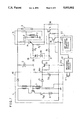
- FIG. 1 is a circuit diagram of electric circuit of a first embodiment of an electric flash apparatus according to the present invention.
- FIG. 2(a), FIG. 2(b) and FIG. 2(c) are wave form charts showing the timing operation of the first embodiment.
- FIG. 3 is a circuit diagram of electric circuit of a second embodiment of the electric flash apparatus according to the present invention.
- FIG. 4 is a circuit diagram of electric circuit of a third embodiment of the electric flash apparatus according to the present invention.
- FIG. 5 is a circuit diagram of electric circuit of a fourth embodiment of the electric flash apparatus according to the present invention.
- FIG. 6(a) and FIG. 6(b) are circuit diagrams of electric circuit of a fifth embodiment of the electric flash apparatus according to the present invention.
- FIG. 7 is a circuit diagram of electric circuit in the prior art.
- FIG. 1 is a circuit diagram of electric circuit of the first embodiment of the electric flash apparatus.
- FIG. 2(a), FIG. 2(b) and FIG. 2(c) are wave form charts showing the timing operation of the first embodiment.
- FIG. 1 corresponding parts and components to the afore-mentioned conventional electric flash apparatus shown in FIG. 7 are shown by the same numerals, and have same functions, respectively.
- a power source circuit 15 comprises a known DC-DC converter circuit as a DC high voltage supply circuit 1 and an operation power supply circuit 16 having an auxiliary winding L of a transformer, a diode D and a capacitor C E for operation power supply.
- An output terminal 16a of the operation power supply circuit 16 is connected to the emitter of a transistor 17 as a switching device.
- the collector of the transistor 17 is connected to the gate of an insulated gate bipolar transistor (hereinafter referred to an I.G.B.T.) 4 of a power transistor through a resistor R 1 .
- the collector of the transistor 17, or a junction point "Z" shown in FIG. 1 is connected to the cathode of a Zener diode 19 as a constant voltage switching circuit which issues output voltage when a voltage is applied thereto.
- a series connection branch 18 comprises the Zener diode 19 and a diode 20 whereof the anode is connected to the anode of the Zener diode 19.
- the cathode of the diode 20 is connected to the gate of thyristor 9 through a resistor R 2 .
- the thyristor 9 is used as a switching device for controlling the operation of a trigger circuit 5.
- the output terminal 16a of the operation power supply circuit 16 is connected to the gate of the I.G.B.T. 4 through the emitter-collector circuit of the transistor 17 and the resistor R 1 , and also to the gate of the thyristor 9 further through the series connection branch 18.
- the ON-signal generating circuit 21 When a synchronous switch 11 is closed for making the flash tube 3 to emit light, the ON-signal generating circuit 21 is actuated to issue an ON signal to the base of the transistor 17. Thereby, the transistor 17 turns ON, and the operation power supply circuit 16 and the gate of the I.G.B.T. 4 are electrically connected. There is no need to say that the ON-signal generating circuit 21 of this first embodiment issues an ON signal of a low level.
- Light emission of the flash tube 3 may be made not only by closing operation of the synchronous switch 11, but also by an electrical signal which is arbitrarily supplied by a camera, etc.
- the ON-signal generating circuit 21 in the first embodiment may be constituted so as to receive such signal. That is, the ON-signal generating circuit 21 is the circuit which issues output signal at the instance when the flash tube 3 is to be flashed.
- the operation of the ON-signal generating circuit 21 is controlled also by an operation of an OFF-signal generating circuit 23 of alight emission control circuit 22.
- the OFF-signal generating circuit 23 comprises a known light control circuit.
- the light control circuit is operated when the integration value of the light reflected from an object due to light emitted from the flash tube 3 reaches a preset value.
- the light control circuit stops the light emission of the flash tube 3 when the light emission is to be stopped.
- a transistor 24 which is a switching device of the light emission control circuit 22 turns ON, and also the ON-signal generating circuit 21 turns OFF and changes its output to the transistor 17 to turn OFF.
- the transistor 24 is connected by its emitter and collector across the gate and the emitter of the I.G.B.T. 4, respectively.
- the I.G.B.T. 4 is turned to OFF state when the transistor 24 turns ON, as a matter of course.
- FIG. 1 operation of the above-mentioned first embodiment is described with reference to the accompanying drawings FIG. 1, FIG. 2(a), FIG. 2(b) and FIG. 2(c).
- the DC-DC converter circuit of the DC high voltage supply circuit 1 is actuated by a low voltage power source E when its power source switch Sw is turned ON. And, the power source circuit 15 starts a known operation of generating a high voltage current.
- the main capacitor 2, the trigger capacitor 6 of the trigger circuit 5 and a power source capacitor C E of the operation power supply circuit 16 are charged with the polarity as shown in FIG. 1.
- the ON-signal generating circuit 21 is operated when the synchronous switch 11 is closed.
- a low level signal is applied at the output terminal 21a which was kept in an electrical open state.
- FIG. 2(a) is a wave form chart showing an electric potential at the junction point "Z". In a part of time close after the point of time t 1 , the I.G.B.T. 4 is insufficiently turned ON, because the electric potential of the junction point "Z" is still in a low level.
- FIG. 2(b) is a wave form chart showing an electric potential at the gate of the thyristor 9.
- the electric potential of the junction point "Z” further increases, and the I.G.B.T. 4 is sufficiently turned ON.
- the Zener diode 19 turns ON.
- the output voltage of the operation power supply circuit 16 is applied to the gate of the thyristor 9. Therefore, the electric potential at the gate of the thyristor 9 becomes high level at the point of time t 2 as shown in FIG. 2(b) whereby the thyristor 9 turns ON.
- FIG. 2(c) is a wave form chart showing a discharge current of the flash tube 3.
- the Zener voltage of the Zener diode 19 is so selected that the potential of the junction point "Z" is higher than a Zener voltage of the Zener diode 19 when the gate potential of the I.G.B.T. 4 is at such potential as to make the I.G.B.T. 4 sufficiently ON. Therefore, even if the output voltage of the operation power supply circuit 16 decreases the electric potential level of the junction point "Z" becomes lower level than the Zener voltage, or even if an ON signal which is increased gradually is applied to the I.G.B.T. 4, the thyristor 9 remains in OFF state until the electric potential level of the junction point "Z" reaches the Zener voltage. In other words, the trigger circuit 5 is operated only after the I.G.B.T. 4 is turned to sufficient ON state.
- both the electric potentials of the gate of the I.G.B.T. 4 and the gate of the thyristor 9 are kept in low level (L).
- L low level
- the gate and the emitter of the I.G.B.T. 4 are Shortcircuitted by the actuated transistor 24.
- the I.G.B.T. 4 turns OFF, and the current flowing in the flash tube 3 is instantly cut off at the point of time t 3 and light emission is stopped as shown in FIG. 2(c).
- the trigger circuit 5 of the first embodiment is actuated by turning ON of the thyristor 9.
- the ON state of the thyristor 9 is forced by operating of the series connection branch 18 having the Zener diode 19 which is changed to ON state at above the preset constant voltage when the I.G.B.T. 4 sufficiently turns ON.
- the trigger circuit 5 when the trigger circuit 5 is operated, the voltage which actuates the I.G.B.T. 4 to sufficiently turn ON is applied to the I.G.B.T. 4 by the operation of the series connection branch 18. Accordingly, the trigger circuit 5 is operated efficiently, and the I.G.B.T. 4 of the power transistor is prevented from breaking down.
- a resistor R shown in FIG. 1 by a dotted line may be connected in parallel to the I.G.B.T. 4 in order to prevent the undesirable ON operation, which is induced by a stray capacitance of the I.G.B.T. 4 when the output voltage of the operation power supply circuit 16 is applied to the gate of the I.G.B.T. 4.
- I.G.B.T. 4 as a power transistor is used in the first embodiment, a field effect transistor (FET) or a general power transistor can be used instead of the I.G.B.T. 4.
- FET field effect transistor
- FIG. 3 is a circuit diagram of electric circuit of the second embodiment of the electric flash apparatus in accordance with the present invention. Corresponding parts and components to the first embodiment are shown by the same numeral and marks, and the description thereon made in the first embodiment similarly apply.
- FIG. 4 is a circuit diagram of electric circuit of a third embodiment of the electric flash apparatus in accordance with the present invention. Corresponding parts and components to the first embodiment are shown by the same numerals and marks, and the description thereon made in the first embodiment similarly apply. Differences and features of this third embodiment from the first embodiment are as follows.
- the cathode of the Zener diode 19 as a constant voltage switching circuit which issues output voltage when a voltage is applied thereto is directly connected by one end to the gate of the I.G.B.T. 4.
- the cathode of the Zener diode 19 is connected to the collector of the transistor 17 through the resistor R 1 .
- the voltage to be applied to the gate of the I.G.B.T. 4 is accurately detected by using a Zener voltage.
- a signal of the OFF-signal generating circuit 23 of the emission control circuit 22 is not transmitted to the ON-signal generating circuit 21 in the third embodiment. Therefore, the operations of the OFF-signal generating circuit 23 and the ON-signal generating circuit 21 are independent from each other.
- the duty time of the ON signal which is issued by the ON-signal generating circuit 21, is selected to have a predetermined interval determined considering the whole discharge time interval of the flash tube 3.
- FIG. 5 is a circuit diagram of electric circuit of a fourth embodiment of the electric flash apparatus in accordance with the present invention. Corresponding parts and components to the first embodiment are shown by the same numerals and marks, and the description thereon made in the first embodiment similarly apply. Differences and features of this fourth embodiment from the first embodiment are as follows.
- the cathode of the thyristor 9, which is a switching device for controlling the operation of the trigger circuit 5, is connected directly to the grounds.
- the diode 20, which is shown in FIG. 1 of the first embodiment, is not provided in this fourth embodiment of FIG. 5.
- the cathode of the thyristor 9 is directly connected to the collector of the I.G.B.T. 4, and hence, the diode 20 is provided to prevent undesirable current from the flash tube 3 through the cathode and the gate of the thyristor 9 to the Zener diode 19.
- the above-mentioned reverse current is not generated because the cathode of the thyristor 9 is grounded, and hence there is no need of a series connection of a diode to the Zener diode 19, as in FIG. 1.
- FIG. 6(a) and FIG. 6(b) are circuit diagrams of electric circuit of a fifth embodiment of the electric flash apparatus in accordance with the present invention. Corresponding parts and components to the first embodiment are shown by the same numerals and marks.
- a switching circuit 25 which turns at a preset constant voltage is provided instead of the Zener diode 19 of the afore-mentioned embodiments.
- the switching circuit 25 comprises a comparator 26, a reference power source 27 and resistors 28, 29.
- the output power of the operation power supply circuit 16 passes through the switching circuit 25 and is applied to the gate of the thyristor 9.
- Corresponding parts and components to the first embodiment are shown by the same numerals and marks, and the description thereon made in the first embodiment similarly apply. Differences and features of this fifth embodiment from the first embodiment are as follows.
- a reference voltage of a reference power source 27 is applied to an inverting input terminal 26b of the comparator 26.
- the output voltage of the output terminal 26c of the comparator 26 is inverted and becomes high level signal.
- the above-mentioned high level signal of the output terminal 26c is applied to the gate of the thyristor 9 through the diode 20 and the resistor R 2 in case of the embodiment shown in FIG. 6(a).
- the high level signal which is issued from the comparator 26 is applied to the gate of it through the resistor R 2 .
- the thyristor 9 turns ON in each case.
- the thyristor 9 can be turned to ON state certainly after the turning ON of the I.G.B.T. 4, similarly to the afore-mentioned embodiments.
- the trigger circuit 5 is operated efficiently, and the I.G.B.T. 4 of the power transistor is prevented from breaking down.
- the above-mentioned switching circuit 25 which turns at the preset constant voltage is coupled to the operation power supply circuit 16 through the transistor 17. Therefore, the switching circuit 25 is operated only when the transistor 17 is in ON state.
- the reference power source 27 for issuing a reference voltage is constituted such that it issues the voltage only when the transistor 17 turns ON, the power source can be saved.
Landscapes
- Discharge-Lamp Control Circuits And Pulse- Feed Circuits (AREA)
- Stroboscope Apparatuses (AREA)
Abstract
Description
Claims (10)
Applications Claiming Priority (2)
| Application Number | Priority Date | Filing Date | Title |
|---|---|---|---|
| JP1078887A JP2584051B2 (en) | 1989-03-29 | 1989-03-29 | Strobe device |
| JP1-78887 | 1989-03-29 |
Publications (1)
| Publication Number | Publication Date |
|---|---|
| US5053802A true US5053802A (en) | 1991-10-01 |
Family
ID=13674320
Family Applications (1)
| Application Number | Title | Priority Date | Filing Date |
|---|---|---|---|
| US07/503,180 Expired - Lifetime US5053802A (en) | 1989-03-29 | 1990-03-28 | Electric flash apparatus |
Country Status (2)
| Country | Link |
|---|---|
| US (1) | US5053802A (en) |
| JP (1) | JP2584051B2 (en) |
Cited By (2)
| Publication number | Priority date | Publication date | Assignee | Title |
|---|---|---|---|---|
| US5532555A (en) * | 1994-03-07 | 1996-07-02 | Olympus Optical Co., Ltd. | Electronic flash apparatus using gate controlled switching device directly driven by CPU |
| US20040051163A1 (en) * | 2002-09-12 | 2004-03-18 | Mitsubishi Denki Kabushiki Kaisha | Strobe light control circuit and IGBT device |
Citations (3)
| Publication number | Priority date | Publication date | Assignee | Title |
|---|---|---|---|---|
| US4697906A (en) * | 1985-09-27 | 1987-10-06 | West Electric Company, Ltd. | Electric flash device |
| JPS63129327A (en) * | 1986-11-19 | 1988-06-01 | West Electric Co Ltd | Strobe lighting device for photography |
| US4839686A (en) * | 1987-07-10 | 1989-06-13 | Minolta Camera Kabushiki Kaisha | Flash device |
-
1989
- 1989-03-29 JP JP1078887A patent/JP2584051B2/en not_active Expired - Fee Related
-
1990
- 1990-03-28 US US07/503,180 patent/US5053802A/en not_active Expired - Lifetime
Patent Citations (3)
| Publication number | Priority date | Publication date | Assignee | Title |
|---|---|---|---|---|
| US4697906A (en) * | 1985-09-27 | 1987-10-06 | West Electric Company, Ltd. | Electric flash device |
| JPS63129327A (en) * | 1986-11-19 | 1988-06-01 | West Electric Co Ltd | Strobe lighting device for photography |
| US4839686A (en) * | 1987-07-10 | 1989-06-13 | Minolta Camera Kabushiki Kaisha | Flash device |
Cited By (7)
| Publication number | Priority date | Publication date | Assignee | Title |
|---|---|---|---|---|
| US5532555A (en) * | 1994-03-07 | 1996-07-02 | Olympus Optical Co., Ltd. | Electronic flash apparatus using gate controlled switching device directly driven by CPU |
| US20040051163A1 (en) * | 2002-09-12 | 2004-03-18 | Mitsubishi Denki Kabushiki Kaisha | Strobe light control circuit and IGBT device |
| US6879024B2 (en) * | 2002-09-12 | 2005-04-12 | Renesas Technology Corp. | Strobe light control circuit and IGBT device |
| US20050145880A1 (en) * | 2002-09-12 | 2005-07-07 | Renesas Technology Corp. | Strobe light control circuit and IGBT device |
| US20060226433A1 (en) * | 2002-09-12 | 2006-10-12 | Renesas Technology Corp. | Strobe light control circuit and IGBT device |
| US7230324B2 (en) | 2002-09-12 | 2007-06-12 | Renesas Technology Corp. | Strobe light control circuit and IGBT device |
| US7385278B2 (en) | 2002-09-12 | 2008-06-10 | Renesas Technology Corp. | Strobe light control circuit and IGBT device |
Also Published As
| Publication number | Publication date |
|---|---|
| JP2584051B2 (en) | 1997-02-19 |
| JPH02256037A (en) | 1990-10-16 |
Similar Documents
| Publication | Publication Date | Title |
|---|---|---|
| US4275335A (en) | Constant light intensity electronic flash device | |
| US4697906A (en) | Electric flash device | |
| US5111233A (en) | Electronic flashing device | |
| US5053802A (en) | Electric flash apparatus | |
| US5107292A (en) | Electronic flash unit | |
| US5187410A (en) | Electronic flash device | |
| US4393335A (en) | Electronic flash device | |
| US4374345A (en) | Electronic flash apparatus | |
| US4382211A (en) | Electric flash device | |
| US4942340A (en) | Arrangement for displaying operation of booster circuit for flash device camera | |
| KR100189815B1 (en) | Flash control circuit | |
| US5752102A (en) | Electronic flashing device | |
| US5038080A (en) | Electric flash apparatus | |
| JP3167353B2 (en) | Flash light emitting device | |
| US5004958A (en) | Strobe apparatus | |
| JP2506692B2 (en) | Photo flash device | |
| US4301392A (en) | Electronic flash system capable of automatic flash duration control | |
| JP2570109Y2 (en) | Light emission control circuit of electronic flash device | |
| JPH0220088B2 (en) | ||
| US4155031A (en) | Electronic flash apparatus | |
| JP2506674B2 (en) | Strobe device | |
| US3703662A (en) | High speed quenching arrangement for a flash device | |
| US4082982A (en) | Automatic electronic flash device | |
| JP2548367B2 (en) | Strobe device | |
| JP2778778B2 (en) | Dimmable strobe control circuit |
Legal Events
| Date | Code | Title | Description |
|---|---|---|---|
| AS | Assignment |
Owner name: WEST ELECTRIC COMPANY, LTD., JAPAN Free format text: ASSIGNMENT OF ASSIGNORS INTEREST.;ASSIGNOR:HIRATA, SHINJI;REEL/FRAME:005326/0910 Effective date: 19900420 |
|
| STCF | Information on status: patent grant |
Free format text: PATENTED CASE |
|
| FEPP | Fee payment procedure |
Free format text: PAYOR NUMBER ASSIGNED (ORIGINAL EVENT CODE: ASPN); ENTITY STATUS OF PATENT OWNER: LARGE ENTITY |
|
| FPAY | Fee payment |
Year of fee payment: 4 |
|
| FPAY | Fee payment |
Year of fee payment: 8 |
|
| FPAY | Fee payment |
Year of fee payment: 12 |
|
| AS | Assignment |
Owner name: PANASONIC PHOTO & LIGHTING CO., LTD., JAPAN Free format text: CHANGE OF NAME;ASSIGNOR:WEST ELECTRIC CO., LTD.;REEL/FRAME:022006/0298 Effective date: 20060401 |