US4959112A - Selective scribing of materials - Google Patents
Selective scribing of materials Download PDFInfo
- Publication number
- US4959112A US4959112A US07/005,616 US561687A US4959112A US 4959112 A US4959112 A US 4959112A US 561687 A US561687 A US 561687A US 4959112 A US4959112 A US 4959112A
- Authority
- US
- United States
- Prior art keywords
- tip
- heated
- scribing
- patterning
- accordance
- Prior art date
- Legal status (The legal status is an assumption and is not a legal conclusion. Google has not performed a legal analysis and makes no representation as to the accuracy of the status listed.)
- Expired - Fee Related
Links
- 239000000463 material Substances 0.000 title claims abstract description 32
- 238000005520 cutting process Methods 0.000 claims abstract description 12
- 238000000034 method Methods 0.000 claims description 23
- 229910052782 aluminium Inorganic materials 0.000 claims description 14
- XAGFODPZIPBFFR-UHFFFAOYSA-N aluminium Chemical compound [Al] XAGFODPZIPBFFR-UHFFFAOYSA-N 0.000 claims description 14
- 238000010438 heat treatment Methods 0.000 claims description 13
- 238000000059 patterning Methods 0.000 claims description 9
- 239000004020 conductor Substances 0.000 claims description 7
- 230000003647 oxidation Effects 0.000 claims description 7
- 238000007254 oxidation reaction Methods 0.000 claims description 7
- 229910021417 amorphous silicon Inorganic materials 0.000 claims description 6
- QVGXLLKOCUKJST-UHFFFAOYSA-N atomic oxygen Chemical compound [O] QVGXLLKOCUKJST-UHFFFAOYSA-N 0.000 claims description 6
- 229910052760 oxygen Inorganic materials 0.000 claims description 6
- 239000001301 oxygen Substances 0.000 claims description 6
- 239000004065 semiconductor Substances 0.000 claims description 6
- 238000000926 separation method Methods 0.000 claims description 6
- 239000000758 substrate Substances 0.000 claims description 4
- XOLBLPGZBRYERU-UHFFFAOYSA-N tin dioxide Chemical compound O=[Sn]=O XOLBLPGZBRYERU-UHFFFAOYSA-N 0.000 claims description 4
- 230000000694 effects Effects 0.000 claims description 3
- 229910001887 tin oxide Inorganic materials 0.000 claims description 2
- 239000010410 layer Substances 0.000 description 14
- 229910052751 metal Inorganic materials 0.000 description 7
- 239000002184 metal Substances 0.000 description 6
- 230000008030 elimination Effects 0.000 description 3
- 238000003379 elimination reaction Methods 0.000 description 3
- 238000005299 abrasion Methods 0.000 description 2
- 239000002253 acid Substances 0.000 description 2
- 230000002411 adverse Effects 0.000 description 2
- 229910045601 alloy Inorganic materials 0.000 description 2
- 239000000956 alloy Substances 0.000 description 2
- 238000001035 drying Methods 0.000 description 2
- 238000005530 etching Methods 0.000 description 2
- 239000011521 glass Substances 0.000 description 2
- 239000012212 insulator Substances 0.000 description 2
- 229910052762 osmium Inorganic materials 0.000 description 2
- SYQBFIAQOQZEGI-UHFFFAOYSA-N osmium atom Chemical compound [Os] SYQBFIAQOQZEGI-UHFFFAOYSA-N 0.000 description 2
- 229910052594 sapphire Inorganic materials 0.000 description 2
- 239000010980 sapphire Substances 0.000 description 2
- 229910052710 silicon Inorganic materials 0.000 description 2
- 239000010703 silicon Substances 0.000 description 2
- 229910000975 Carbon steel Inorganic materials 0.000 description 1
- 229910000997 High-speed steel Inorganic materials 0.000 description 1
- KJTLSVCANCCWHF-UHFFFAOYSA-N Ruthenium Chemical compound [Ru] KJTLSVCANCCWHF-UHFFFAOYSA-N 0.000 description 1
- 229910000831 Steel Inorganic materials 0.000 description 1
- 238000005275 alloying Methods 0.000 description 1
- 239000004411 aluminium Substances 0.000 description 1
- 230000015572 biosynthetic process Effects 0.000 description 1
- 230000015556 catabolic process Effects 0.000 description 1
- 239000000919 ceramic Substances 0.000 description 1
- 239000011248 coating agent Substances 0.000 description 1
- 238000000576 coating method Methods 0.000 description 1
- 239000012141 concentrate Substances 0.000 description 1
- 238000010276 construction Methods 0.000 description 1
- 238000011109 contamination Methods 0.000 description 1
- 229910052593 corundum Inorganic materials 0.000 description 1
- 239000010431 corundum Substances 0.000 description 1
- 238000006731 degradation reaction Methods 0.000 description 1
- 238000009792 diffusion process Methods 0.000 description 1
- 238000004519 manufacturing process Methods 0.000 description 1
- 239000007769 metal material Substances 0.000 description 1
- 150000002739 metals Chemical class 0.000 description 1
- 238000012986 modification Methods 0.000 description 1
- 230000004048 modification Effects 0.000 description 1
- TWNQGVIAIRXVLR-UHFFFAOYSA-N oxo(oxoalumanyloxy)alumane Chemical compound O=[Al]O[Al]=O TWNQGVIAIRXVLR-UHFFFAOYSA-N 0.000 description 1
- BASFCYQUMIYNBI-UHFFFAOYSA-N platinum Chemical group [Pt] BASFCYQUMIYNBI-UHFFFAOYSA-N 0.000 description 1
- 238000010791 quenching Methods 0.000 description 1
- 229910052707 ruthenium Inorganic materials 0.000 description 1
- 238000006748 scratching Methods 0.000 description 1
- 230000002393 scratching effect Effects 0.000 description 1
- 238000003892 spreading Methods 0.000 description 1
- 239000010959 steel Substances 0.000 description 1
- 239000002344 surface layer Substances 0.000 description 1
Images

Classifications
-
- B—PERFORMING OPERATIONS; TRANSPORTING
- B25—HAND TOOLS; PORTABLE POWER-DRIVEN TOOLS; MANIPULATORS
- B25H—WORKSHOP EQUIPMENT, e.g. FOR MARKING-OUT WORK; STORAGE MEANS FOR WORKSHOPS
- B25H7/00—Marking-out or setting-out work
- B25H7/04—Devices, e.g. scribers, for marking
- B25H7/045—Devices, e.g. scribers, for marking characterised by constructional details of the marking elements
-
- Y—GENERAL TAGGING OF NEW TECHNOLOGICAL DEVELOPMENTS; GENERAL TAGGING OF CROSS-SECTIONAL TECHNOLOGIES SPANNING OVER SEVERAL SECTIONS OF THE IPC; TECHNICAL SUBJECTS COVERED BY FORMER USPC CROSS-REFERENCE ART COLLECTIONS [XRACs] AND DIGESTS
- Y10—TECHNICAL SUBJECTS COVERED BY FORMER USPC
- Y10T—TECHNICAL SUBJECTS COVERED BY FORMER US CLASSIFICATION
- Y10T156/00—Adhesive bonding and miscellaneous chemical manufacture
- Y10T156/10—Methods of surface bonding and/or assembly therefor
- Y10T156/1052—Methods of surface bonding and/or assembly therefor with cutting, punching, tearing or severing
- Y10T156/1062—Prior to assembly
- Y10T156/1064—Partial cutting [e.g., grooving or incising]
-
- Y—GENERAL TAGGING OF NEW TECHNOLOGICAL DEVELOPMENTS; GENERAL TAGGING OF CROSS-SECTIONAL TECHNOLOGIES SPANNING OVER SEVERAL SECTIONS OF THE IPC; TECHNICAL SUBJECTS COVERED BY FORMER USPC CROSS-REFERENCE ART COLLECTIONS [XRACs] AND DIGESTS
- Y10—TECHNICAL SUBJECTS COVERED BY FORMER USPC
- Y10T—TECHNICAL SUBJECTS COVERED BY FORMER US CLASSIFICATION
- Y10T156/00—Adhesive bonding and miscellaneous chemical manufacture
- Y10T156/10—Methods of surface bonding and/or assembly therefor
- Y10T156/1052—Methods of surface bonding and/or assembly therefor with cutting, punching, tearing or severing
- Y10T156/108—Flash, trim or excess removal
-
- Y—GENERAL TAGGING OF NEW TECHNOLOGICAL DEVELOPMENTS; GENERAL TAGGING OF CROSS-SECTIONAL TECHNOLOGIES SPANNING OVER SEVERAL SECTIONS OF THE IPC; TECHNICAL SUBJECTS COVERED BY FORMER USPC CROSS-REFERENCE ART COLLECTIONS [XRACs] AND DIGESTS
- Y10—TECHNICAL SUBJECTS COVERED BY FORMER USPC
- Y10T—TECHNICAL SUBJECTS COVERED BY FORMER US CLASSIFICATION
- Y10T156/00—Adhesive bonding and miscellaneous chemical manufacture
- Y10T156/10—Methods of surface bonding and/or assembly therefor
- Y10T156/1052—Methods of surface bonding and/or assembly therefor with cutting, punching, tearing or severing
- Y10T156/1082—Partial cutting bonded sandwich [e.g., grooving or incising]
-
- Y—GENERAL TAGGING OF NEW TECHNOLOGICAL DEVELOPMENTS; GENERAL TAGGING OF CROSS-SECTIONAL TECHNOLOGIES SPANNING OVER SEVERAL SECTIONS OF THE IPC; TECHNICAL SUBJECTS COVERED BY FORMER USPC CROSS-REFERENCE ART COLLECTIONS [XRACs] AND DIGESTS
- Y10—TECHNICAL SUBJECTS COVERED BY FORMER USPC
- Y10T—TECHNICAL SUBJECTS COVERED BY FORMER US CLASSIFICATION
- Y10T83/00—Cutting
- Y10T83/02—Other than completely through work thickness
- Y10T83/0304—Grooving
-
- Y—GENERAL TAGGING OF NEW TECHNOLOGICAL DEVELOPMENTS; GENERAL TAGGING OF CROSS-SECTIONAL TECHNOLOGIES SPANNING OVER SEVERAL SECTIONS OF THE IPC; TECHNICAL SUBJECTS COVERED BY FORMER USPC CROSS-REFERENCE ART COLLECTIONS [XRACs] AND DIGESTS
- Y10—TECHNICAL SUBJECTS COVERED BY FORMER USPC
- Y10T—TECHNICAL SUBJECTS COVERED BY FORMER US CLASSIFICATION
- Y10T83/00—Cutting
- Y10T83/02—Other than completely through work thickness
- Y10T83/0333—Scoring
- Y10T83/0341—Processes
-
- Y—GENERAL TAGGING OF NEW TECHNOLOGICAL DEVELOPMENTS; GENERAL TAGGING OF CROSS-SECTIONAL TECHNOLOGIES SPANNING OVER SEVERAL SECTIONS OF THE IPC; TECHNICAL SUBJECTS COVERED BY FORMER USPC CROSS-REFERENCE ART COLLECTIONS [XRACs] AND DIGESTS
- Y10—TECHNICAL SUBJECTS COVERED BY FORMER USPC
- Y10T—TECHNICAL SUBJECTS COVERED BY FORMER US CLASSIFICATION
- Y10T83/00—Cutting
- Y10T83/04—Processes
- Y10T83/0405—With preparatory or simultaneous ancillary treatment of work
- Y10T83/041—By heating or cooling
- Y10T83/0414—At localized area [e.g., line of separation]
-
- Y—GENERAL TAGGING OF NEW TECHNOLOGICAL DEVELOPMENTS; GENERAL TAGGING OF CROSS-SECTIONAL TECHNOLOGIES SPANNING OVER SEVERAL SECTIONS OF THE IPC; TECHNICAL SUBJECTS COVERED BY FORMER USPC CROSS-REFERENCE ART COLLECTIONS [XRACs] AND DIGESTS
- Y10—TECHNICAL SUBJECTS COVERED BY FORMER USPC
- Y10T—TECHNICAL SUBJECTS COVERED BY FORMER US CLASSIFICATION
- Y10T83/00—Cutting
- Y10T83/283—With means to control or modify temperature of apparatus or work
- Y10T83/293—Of tool
Definitions
- Modern photovoltaic panels which convert incident electromagnetic energy into electrical power, desirably have a panel construction in which a glass substrate supports an overlying transparent conductive layer, with a further overlying layer of amorphous silicon and an outer layer of metal such as aluminum.
- the panel is formed by interconnecting a number of individual cells. The latter are formed on the substrate by the scribing or patterning of the laminar structure at various stages of production. In the final stage, an overall coating of metal, such as aluminum, is applied, and it is necessary to scribe or pattern the aluminum in order to separate the adjoining cells from one another.
- Heating that extends to the underlying semiconductor is avoided to prevent damage to the semiconductor.
- the underlying semiconductor e.g. hydrogenated amorphous silicon
- Heating above 200° C. to 300° C. can cause irreparable damage to the semiconductor.
- Heating of the aluminum can also cause contamination by diffusion of aluminun into the semiconductor.
- a related object is to facilitate the selective scribing of photovoltaic panels, particularly the outer metallic contact layers that are involved in such panels.
- Another object of the invention is to achieve scribing with less complexity and, consequently, less time consumption than is involved with conventional photo-resist and laser scribing procedures.
- a further object of the invention is to increase the reliability of scribing and avoid the incomplete cuts or overcuts that are frequently associated with photo-resist and laser scribing procedures.
- Still another object of the invention is to avoid the need for applying "resist" materials, the drying of those materials, and their selective removal in order to achieve desired scribing of materials.
- An associated object is to eliminate the need for acid etching and final removal of the resist material.
- Yet another object is to avoid the adverse consequences of heating during the scribing of materials, particularly by cutting tips in which heating can damage solar panels.
- a still further object is to avoid the need for excessive pressure during scribing.
- the invention provides for placing a material to be scribed in a gaseous atmosphere and contacting the surface of the material with a non-cutting heated tip.
- the heated tip is rounded to prevent cutting and is moved relative to the material, either by moving the tip or the material in accordance with the pattern that is to be scribed.
- the tip is heated during the scribing operation, either continuously at a prescribed level, or discontinuously in order to maintain the average temperature at a prescribed level. Discontinuous heating allows the desired average temperature to be realized quickly. It may take the form of successive pulsing.
- the tip desirably has a longitudinal axis that forms an angle of less than 90° relative to the surface being inscribed.
- inscription by a heated tip is particularly useful for metals such as aluminum.
- the tip is heated and maintained at a temperature above the softening point of the material, so that a tip temperature in the range above about 250° C. is desirable for aluminum.
- the atmosphere in which the tip operates is controlled according to the result desired. If the material is to be oxidized by scribing, the atmosphere includes oxygen. Conversely, where oxidation is to be prevented, the atmosphere is inert.
- the tip has a longitudinal axis which is maintained at an angle of less than 90° in relation to the surface inscribed.
- a plurality of tips can be employed in order to achieve multiple scribes of the material.
- the tip it is desirable for the tip to be maintained in pressure contact with the surface being inscribed without physical cutting.
- a suitable pressure is on the order of 10 3 -10 5 pounds per square inch.
- any shards of metallic material that remain between adjoining sections that have been scribed are burned out by applying a voltage to the adjoining sections.
- the resultant passage of current causes the substantially immediate elimination of the shards and consequently their complete elimination from the scribed structure.
- the rounded tip has an included angle between about 25° and 30°.
- the radius of the tip is initially between about 0.0020 and 0.0025 inches.
- the initial formed tip is desirably further rounded by abrasion, with, for example, tin dioxide, to a working radius of about 0.0040 inches. This is because of the importance of avoiding a sharp or scratching tip.
- the two-step procedure permits precision control over the rounding operation.
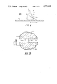
- FIG. 1 is a schematic view illustrating a heated scribing tip in accordance with the invention and an associated metallic layer that is being inscribed;
- FIG. 2 is a side view of an illustrative scribing platform employed in connection with the heated tip of FIG. 1;
- FIG. 3 is a plan view illustrating the burn-out of residual shards that can remain after preliminary scribing in accordance with the invention.
- FIG. 1 shows an illustrative patterning device 10 for inscribing the metallic surface 15 of a photovoltaic laminate 16.
- the device 10 includes a heat source with a rounded conical tip 11t that is secured to a rod 11r.
- the tip 11t is rounded to make it non-cutting.
- the holder for the tip 11t and the rod 11r are of steel.
- the source 11 includes a heater 16' which is sandwiched between cylindrical insulators 17-1 and 17-2.
- the leads 16-1 and 16-2 of the heater 16' extend to an electrical power supply (not shown).
- the insulators 17-1 and 17-2 are desirably of ceramic.
- the laminate 16 shown positioned beneath the heated tip 11t can be a standard photovoltaic panel in which the individual cells are isolated from one another by inscription, for example along the lines 18-1 and 18-2 shown in FIG. 1.
- the line 18-1 was completed on a prior pass and the line 18-2 is in the course of being completed.
- the device 10 with a non-cutting heated tip is mounted in relation to a movable platform 21 at a fixed angle A less than 90 degrees to form the overall scribing machine 20 of FIG. 2.
- the platform 21 is moved in the direction indicated by the arrow B while the laminate 16 is maintained in contact with the tip 10.
- the included angle C of the tip is between about 25 and 30 degrees.
- the radius of the tip is initially between about 0.0020 and 0.0025 inches.
- the machine 20 is provided with an atmosphere that depends upon the effect to be achieved. Where the scribing is to oxidize the patterns formed on the surface 15, the atmosphere contains oxygen. To promote oxidation, the oxygen content is increased above the percentage found in air. Where no oxidation is to take place, the atmosphere is inert, i.e. no oxygen is present.
- the tip 10 When the surface 15 is metallic, the tip 10 is heated above the softening temperature of the metal. In the case of aluminum, this is above about 250° C. and the aluminum is rapidly and sufficiently softened to permit quick and reliable scribes without damaging the underlying layers of the laminate 16. Because the heating of the tip 10 permits rapid separation of the surface layers, there is little time for the transfer of heat laterally. In addition, the separation takes place rapidly because the aluminum layer is comparatively thin, being on the order of a few thousand Angstroms in thickness. There is the further fact that the ordinary substrate for the laminate 16 is a poor heat conductor such as glass and the limited lateral conduction prevents any undesired heating of the amorphous silicon that extends between separations in the aluminum surface. For this purpose, the lateral heating of the amorphous silicon is held to levels below about 200° C. and 300° C. where degradation in photovoltaic performance of amorphous silicon can take place.
- the tip 11t is desirably of osmium, sapphire, or Schaeffer alloys.
- Osmium is a metallic element of the platinum group; sapphire is a transparent corundum (aluminum oxide) and Schaeffer alloy is primarily Ruthenium. High speed and carbon steels are not satisfactory.
- the tip is flattened by221 abrasion, with tin oxide for example, to a working radius of about 0.0040 inches.
- the invention provides for the elimination of the filamentary strands or shards in accordance with FIG. 3.
- a scribed path 31 extends between adjoining scribed metallic sections 32A and 32B.
- two metallic filaments or shards 33-a and 33-b are shown extending between the main section 32A and 32B.
- the residual shards 33-a and 33-b are eliminated by the momentary application of a voltage from a battery 34 through a switch 32 to the sections 32A and 32B.
- the switch 32 When the switch 32 is momentarily closed, the current that flows in the circuit including the battery 34 causes a rapid burn-out of the shards 33-a and 33-b because of their high resistance. It is apparent that the operation is self-quenching because once the shards 33-a and 33-b have been burnt out, the battery 34 is restored to its open circuit condition. To protect the solar cells, the battery is connected to reverse bias the solar cells.
Landscapes
- Engineering & Computer Science (AREA)
- Mechanical Engineering (AREA)
- Photovoltaic Devices (AREA)
Abstract
Description
Claims (16)
Priority Applications (1)
| Application Number | Priority Date | Filing Date | Title |
|---|---|---|---|
| US07/005,616 US4959112A (en) | 1984-11-14 | 1987-01-21 | Selective scribing of materials |
Applications Claiming Priority (2)
| Application Number | Priority Date | Filing Date | Title |
|---|---|---|---|
| US67119984A | 1984-11-14 | 1984-11-14 | |
| US07/005,616 US4959112A (en) | 1984-11-14 | 1987-01-21 | Selective scribing of materials |
Related Parent Applications (1)
| Application Number | Title | Priority Date | Filing Date |
|---|---|---|---|
| US67119984A Continuation-In-Part | 1984-11-14 | 1984-11-14 |
Publications (1)
| Publication Number | Publication Date |
|---|---|
| US4959112A true US4959112A (en) | 1990-09-25 |
Family
ID=26674547
Family Applications (1)
| Application Number | Title | Priority Date | Filing Date |
|---|---|---|---|
| US07/005,616 Expired - Fee Related US4959112A (en) | 1984-11-14 | 1987-01-21 | Selective scribing of materials |
Country Status (1)
| Country | Link |
|---|---|
| US (1) | US4959112A (en) |
Cited By (6)
| Publication number | Priority date | Publication date | Assignee | Title |
|---|---|---|---|---|
| FR2693142A1 (en) * | 1992-07-02 | 1994-01-07 | Peugeot | Numbering procedure and appts. for moulded workpieces - uses computer-controlled heated stylus to mark pattern or mould, e.g. of expanded polystyrene@ |
| US5741557A (en) * | 1993-07-30 | 1998-04-21 | International Business Machines Corporation | Method for depositing metal fine lines on a substrate |
| US20050257653A1 (en) * | 2004-05-06 | 2005-11-24 | Erich Weidmann | Thermal severing scissors with a ceramic mount |
| CN105773564A (en) * | 2016-01-13 | 2016-07-20 | 哈尔滨飞机工业集团有限责任公司 | Tool assembly used for scribing die cutting line of numerical control machine tool |
| CN114274115A (en) * | 2021-11-25 | 2022-04-05 | 浙江省交通运输科学研究院 | Pipe marking device and method based on end face positioning |
| US20220281128A1 (en) * | 2021-03-06 | 2022-09-08 | James Timothy Struck | Voice Writing Machine |
Citations (7)
| Publication number | Priority date | Publication date | Assignee | Title |
|---|---|---|---|---|
| US2743348A (en) * | 1952-08-30 | 1956-04-24 | Fairchild Camera Instr Co | Engraving stylus |
| US3538292A (en) * | 1969-01-13 | 1970-11-03 | Texas Instruments Inc | Apparatus for severing circuit patterns on and forming conductive connections through a circuit board |
| US3555950A (en) * | 1968-06-08 | 1971-01-19 | Philips Corp | Apparatus for cutting a drawing in a layer of synthetic material |
| US3673030A (en) * | 1969-02-13 | 1972-06-27 | Comptoir Europ De Distribution | Method for manufacturing articles made of flexible plastic |
| US4388134A (en) * | 1982-04-28 | 1983-06-14 | Diving Unlimited International, Inc. | Underwater diver's dry suit and method of sealing |
| US4519864A (en) * | 1982-07-14 | 1985-05-28 | Mineo Isobe | Method of making a paper pattern for dyeing |
| US4594499A (en) * | 1983-01-21 | 1986-06-10 | Protocol Engineering Limited | Apparatus for producing a line of separation in a plastic work surface |
-
1987
- 1987-01-21 US US07/005,616 patent/US4959112A/en not_active Expired - Fee Related
Patent Citations (7)
| Publication number | Priority date | Publication date | Assignee | Title |
|---|---|---|---|---|
| US2743348A (en) * | 1952-08-30 | 1956-04-24 | Fairchild Camera Instr Co | Engraving stylus |
| US3555950A (en) * | 1968-06-08 | 1971-01-19 | Philips Corp | Apparatus for cutting a drawing in a layer of synthetic material |
| US3538292A (en) * | 1969-01-13 | 1970-11-03 | Texas Instruments Inc | Apparatus for severing circuit patterns on and forming conductive connections through a circuit board |
| US3673030A (en) * | 1969-02-13 | 1972-06-27 | Comptoir Europ De Distribution | Method for manufacturing articles made of flexible plastic |
| US4388134A (en) * | 1982-04-28 | 1983-06-14 | Diving Unlimited International, Inc. | Underwater diver's dry suit and method of sealing |
| US4519864A (en) * | 1982-07-14 | 1985-05-28 | Mineo Isobe | Method of making a paper pattern for dyeing |
| US4594499A (en) * | 1983-01-21 | 1986-06-10 | Protocol Engineering Limited | Apparatus for producing a line of separation in a plastic work surface |
Cited By (7)
| Publication number | Priority date | Publication date | Assignee | Title |
|---|---|---|---|---|
| FR2693142A1 (en) * | 1992-07-02 | 1994-01-07 | Peugeot | Numbering procedure and appts. for moulded workpieces - uses computer-controlled heated stylus to mark pattern or mould, e.g. of expanded polystyrene@ |
| US5741557A (en) * | 1993-07-30 | 1998-04-21 | International Business Machines Corporation | Method for depositing metal fine lines on a substrate |
| US5973295A (en) * | 1993-07-30 | 1999-10-26 | International Business Machines Corporation | Heated tool positioned in the X,Y, and 2-directions for depositing fine lines on a substrate |
| US20050257653A1 (en) * | 2004-05-06 | 2005-11-24 | Erich Weidmann | Thermal severing scissors with a ceramic mount |
| CN105773564A (en) * | 2016-01-13 | 2016-07-20 | 哈尔滨飞机工业集团有限责任公司 | Tool assembly used for scribing die cutting line of numerical control machine tool |
| US20220281128A1 (en) * | 2021-03-06 | 2022-09-08 | James Timothy Struck | Voice Writing Machine |
| CN114274115A (en) * | 2021-11-25 | 2022-04-05 | 浙江省交通运输科学研究院 | Pipe marking device and method based on end face positioning |
Similar Documents
| Publication | Publication Date | Title |
|---|---|---|
| EP1544172B1 (en) | Mechanical scribe device | |
| US4959112A (en) | Selective scribing of materials | |
| US4862227A (en) | Semiconductor device and its manufacturing method | |
| JPH0533548B2 (en) | ||
| US9114467B2 (en) | Method of smoothing and/or bevelling an edge of a substrate | |
| WO2023083528A1 (en) | Method and device for processing a solar module | |
| KR860700225A (en) | Cutting method of amorphous alloy using heat | |
| JPS5721230A (en) | Positioning method in wire cut electric discharge processing | |
| JPH10125632A (en) | Method and apparatus for laser etching | |
| JPH0713954B2 (en) | Liquid crystal display device manufacturing method | |
| US20120318776A1 (en) | Method and apparatus for machining a workpiece | |
| US1512788A (en) | Electric-arc-welding apparatus and method of operating the same | |
| CN103367535A (en) | Tool and method for processing groove of thin film solar cell, and groove processing device | |
| CN114985955B (en) | Double-scribing laser edge cleaning process | |
| US3607448A (en) | Chemical milling of silicon carbide | |
| Schneller et al. | Study of the laser scribing of molybdenum thin films fabricated using different deposition techniques | |
| JP2540501B2 (en) | Laser processing method | |
| US2053881A (en) | Selenium cell manufacture | |
| TW379337B (en) | Method for fabrication of thin film resistor | |
| JPS60102288A (en) | Laser working method of film on organic resin | |
| JPS6456817A (en) | Heat treatment method | |
| JPS5750454A (en) | Etching for soldered electrode | |
| JPH03291185A (en) | Working method for ceramics | |
| JPS6384073A (en) | Optical processing method of translucent conductive film | |
| JPS61276795A (en) | Laser scribing method for hybrid integrated circuit device |
Legal Events
| Date | Code | Title | Description |
|---|---|---|---|
| FPAY | Fee payment |
Year of fee payment: 4 |
|
| AS | Assignment |
Owner name: ENERGETICS JUNGERE CORP., DISTRICT OF COLUMBIA Free format text: ASSIGNMENT OF ASSIGNORS INTEREST;ASSIGNOR:SHEET METAL WORKERS' NATIONAL PENSION FUND,THE;REEL/FRAME:008621/0620 Effective date: 19961014 Owner name: SHEET METAL WORKERS' NATIONAL PENSION FUND, THE, V Free format text: ASSIGNMENT OF ASSIGNORS INTEREST;ASSIGNOR:CHRONAR CORPORATION;REEL/FRAME:008621/0970 Effective date: 19940726 |
|
| AS | Assignment |
Owner name: BP SOLAR, INC., OHIO Free format text: ASSIGNMENT OF ASSIGNORS INTEREST;ASSIGNOR:ENERGETICS JUNGERE CORP.;REEL/FRAME:008732/0195 Effective date: 19961015 |
|
| FEPP | Fee payment procedure |
Free format text: PAT HLDR NO LONGER CLAIMS SMALL ENT STAT AS INDIV INVENTOR (ORIGINAL EVENT CODE: LSM1); ENTITY STATUS OF PATENT OWNER: LARGE ENTITY |
|
| FPAY | Fee payment |
Year of fee payment: 8 |
|
| REMI | Maintenance fee reminder mailed | ||
| LAPS | Lapse for failure to pay maintenance fees | ||
| STCH | Information on status: patent discontinuation |
Free format text: PATENT EXPIRED DUE TO NONPAYMENT OF MAINTENANCE FEES UNDER 37 CFR 1.362 |
|
| FP | Lapsed due to failure to pay maintenance fee |
Effective date: 20020925 |