US4937726A - High forward blocking voltage protection circuit - Google Patents
High forward blocking voltage protection circuit Download PDFInfo
- Publication number
- US4937726A US4937726A US07/373,681 US37368189A US4937726A US 4937726 A US4937726 A US 4937726A US 37368189 A US37368189 A US 37368189A US 4937726 A US4937726 A US 4937726A
- Authority
- US
- United States
- Prior art keywords
- semiconductor switch
- conducting
- capacitor
- diode
- voltage source
- Prior art date
- Legal status (The legal status is an assumption and is not a legal conclusion. Google has not performed a legal analysis and makes no representation as to the accuracy of the status listed.)
- Expired - Fee Related
Links
Images

Classifications
-
- H—ELECTRICITY
- H03—ELECTRONIC CIRCUITRY
- H03K—PULSE TECHNIQUE
- H03K17/00—Electronic switching or gating, i.e. not by contact-making and –breaking
- H03K17/08—Modifications for protecting switching circuit against overcurrent or overvoltage
- H03K17/081—Modifications for protecting switching circuit against overcurrent or overvoltage without feedback from the output circuit to the control circuit
- H03K17/0814—Modifications for protecting switching circuit against overcurrent or overvoltage without feedback from the output circuit to the control circuit by measures taken in the output circuit
- H03K17/08142—Modifications for protecting switching circuit against overcurrent or overvoltage without feedback from the output circuit to the control circuit by measures taken in the output circuit in field-effect transistor switches
-
- H—ELECTRICITY
- H02—GENERATION; CONVERSION OR DISTRIBUTION OF ELECTRIC POWER
- H02M—APPARATUS FOR CONVERSION BETWEEN AC AND AC, BETWEEN AC AND DC, OR BETWEEN DC AND DC, AND FOR USE WITH MAINS OR SIMILAR POWER SUPPLY SYSTEMS; CONVERSION OF DC OR AC INPUT POWER INTO SURGE OUTPUT POWER; CONTROL OR REGULATION THEREOF
- H02M3/00—Conversion of DC power input into DC power output
- H02M3/22—Conversion of DC power input into DC power output with intermediate conversion into AC
- H02M3/24—Conversion of DC power input into DC power output with intermediate conversion into AC by static converters
- H02M3/28—Conversion of DC power input into DC power output with intermediate conversion into AC by static converters using discharge tubes with control electrode or semiconductor devices with control electrode to produce the intermediate AC
- H02M3/325—Conversion of DC power input into DC power output with intermediate conversion into AC by static converters using discharge tubes with control electrode or semiconductor devices with control electrode to produce the intermediate AC using devices of a triode or a transistor type requiring continuous application of a control signal
- H02M3/335—Conversion of DC power input into DC power output with intermediate conversion into AC by static converters using discharge tubes with control electrode or semiconductor devices with control electrode to produce the intermediate AC using devices of a triode or a transistor type requiring continuous application of a control signal using semiconductor devices only
- H02M3/33569—Conversion of DC power input into DC power output with intermediate conversion into AC by static converters using discharge tubes with control electrode or semiconductor devices with control electrode to produce the intermediate AC using devices of a triode or a transistor type requiring continuous application of a control signal using semiconductor devices only having several active switching elements
-
- H—ELECTRICITY
- H03—ELECTRONIC CIRCUITRY
- H03K—PULSE TECHNIQUE
- H03K17/00—Electronic switching or gating, i.e. not by contact-making and –breaking
- H03K17/51—Electronic switching or gating, i.e. not by contact-making and –breaking characterised by the components used
- H03K17/56—Electronic switching or gating, i.e. not by contact-making and –breaking characterised by the components used by the use, as active elements, of semiconductor devices
- H03K17/687—Electronic switching or gating, i.e. not by contact-making and –breaking characterised by the components used by the use, as active elements, of semiconductor devices the devices being field-effect transistors
- H03K17/689—Electronic switching or gating, i.e. not by contact-making and –breaking characterised by the components used by the use, as active elements, of semiconductor devices the devices being field-effect transistors with galvanic isolation between the control circuit and the output circuit
- H03K17/691—Electronic switching or gating, i.e. not by contact-making and –breaking characterised by the components used by the use, as active elements, of semiconductor devices the devices being field-effect transistors with galvanic isolation between the control circuit and the output circuit using transformer coupling
Definitions
- the present invention relates to arrangements for freeing or protecting a semiconductor switch from high forward blocking voltage stresses, often referred to as voltage spikes or voltage transients, which occur when the semiconductor switch changes from a conducting state to a non-conducting or blocking state. More particularly, the present invention relates to a system which protects the semiconductor switch against such voltage stresses or spikes and which provides for utilization of the energy which creates the voltage spikes, thus increasing the efficiency of the system.
- DE-OS No. 3,609,375 discloses an arrangement for freeing or protecting a semiconductor switch from such high forward blocking voltages by providing a capacitor-diode circuit, called a "snubber", to absorb the energy during turn-off of the semiconductor switch by charging the capacitor of the snubber.
- the diode of this snubber is connected to a current converter transformer, and the capacitor of the snubber is discharged through the current converter transformer and is fed back to a voltage source, e.g. the voltage source driving the load current, by way of a useful impedance.
- oscillator circuits are provided for protecting the semiconductor switches.
- the oscillator circuits are composed of capacitors, inductances and diodes, and although the arrangements according to DE-OS No. 2,644,715 permit utilization of the energy during turn-off of the semiconductor switch, the arrangements require expensive circuitry. Furthmore, the parameters for such circuits are often critical.
- U.S. Pat. No. 4,700,083 discloses a semiconductor switch which is equipped with a voltage limiting device including an oscillator circuit. It is also known to protect a semiconductor switch against excess voltage stresses by equipping it with a so-called RCD network (DE-OS No. 3,538,184; Electronic Design News, May 1981, pages 126-130). When using an RCD network the protection is realized by the dissipation of energy in an ohmic resistor.
- the present invention provides for protection of a semiconductor switch against forward blocking voltage stresses which occur as the switch is turned-off, by storing the energy which would otherwise cause the voltage stresses, and thereafter utilizing the stored energy to increase the efficiency of the system.
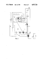
- FIG. 1 is a basic circuit diagram for a semiconductor switch equipped with a protective circuit and employed in a DC/DC converter;
- FIG. 2 is a basic circuit diagram according to FIG. 1 including details of a control circuit St of FIG. 1 for actuating the semiconductor switch;
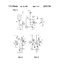
- FIGS. 3, 4, and 5 are modifications to the basic circuit diagram according to FIG. 1.
- a first semiconductor switch T1 is shown connected as a control member in a DC/DC converter.
- a d.c. voltage source Q provides an input voltage.
- An input smoothing capacitor CE is connected across the terminals of the voltage source Q.
- the positive terminal of the voltage source Q is provided to one side of a series combination comprising a diode D1, a power transformer U and the switching path of the first semiconductor switch which, in the present invention, is a field effect transistor T1. More specifically, the positive output of the voltage source is connected to the anode of diode D1, and the cathode of diode D1 is connected to one side of a primary winding of the power transformer.
- Power transformer U constitutes in view of transistor T1 a useful impedance which can be connected to a load circuit of a DC/DC converter.
- power transformer U represents an inductance here the main inductance of a blocking converter.
- the power transformer includes a secondary winding w2 and a smoothing capacitor CG is provided across the secondary winding.
- a conventional diode D3 is provided in the secondary of the power transformer between the winding w2 and the smoothing capacitor CG.
- An output voltage UA is obtained across the terminals of the smoothing capacitor CG as is conventional.
- Transistor T1 is illustrated as a conventional FET, or field effect transistor, having gate, source and drain electrodes.
- a relief circuit --a so-called “snubber" --is provided between the drain electrode of the FET and the positive terminal of the voltage source Q.
- the relief circuit protects the first semiconductor switch against too high a forward blocking voltage stress during turn-off.
- the relief circuit comprises the series combination of a diode D2 and a capacitor C1.
- the diode D2 has its anode connected to the drain of electrode the FET T1, and its cathode connected to one side of the capacitor C1; the other side of the capacitor C1 is connected to the positive terminal of the input voltage source Q.
- the polarity of the diode D2 is such that with field effect transistor T1 in the blocking or non-conducting state, a current will flow through diode D2 to charge capacitor C1.
- the circuit of the present invention includes a second semiconductor switch T2, also illustrated in the preferred embodiment as a field effect transistor having gate, source and drain electrodes as is conventional.
- the drain electrode is connected to the junction of the diode D2 and the capacitor C1
- the source electrode is connected to the junction of the diode D1 and the primary winding w1 of the load. This circuit arrangement permits the capacitor C1 to discharge through the load.
- the relief circuit is disposed between the drain electrode of FET T1 and the positive terminal of input voltage source Q. It is, of course, contemplated to position the relief circuit between the drain electrode and the negative terminal of the voltage surce Q, in which case, it is merely necessary to slightly modify the circuit as will be understood by those of ordinary skill in the art.
- FIG. 3 One of such modifications is shown in FIG. 3.
- the relief circuit is disposed between the drain electrode of FET T1 and the negative terminal of input voltage source Q. All other components are arranged as shown in FIG. 1.
- the drain electrode of FET T1 is connected to the positive terminal of voltage source Q.
- the source electrode of FET T1 is in series connected via winding w1 and diode D1 to the negative terminal of voltage source Q.
- the series combination of diode D2 and capacitor C1 as part of the relief circuit is arranged between the source electrode of FET T1 and the negative terminal of voltage source Q.
- Field effect transistor T2 has its drain electrode connected to the junction of winding w1 with the anode of diode D1 and its source electrode connected to the junction of capacitor C1 with the anode of diode D2.
- FIG. 5 is similar to the embodiment of FIG. 4 with the only difference that capacitor C1 is connected to the positive terminal of voltage source Q.
- FIGS. 1 and 4 are advantageous in view of minimizing voltage stresses of capacitor C1.
- the embodiments of FIGS. 2 and 3 are advantageous in view of protecting FET T1 from high voltage stresses.
- the embodiments of FIGS. 1 or 4 can be for high voltage applications preferably.
- field effect transistor T1 is truned on (i.e., in a conducting state) by means of a control circuit St providing an input to the gate electrode of FET T1
- current flows through the diode D1, through the winding w1 on the primary side of power transformer U, and through the switching path of field effect transistor T1.
- This energizes the primary side of the power transformer.
- field effect transistor T1 is opened (i.e., blocked or turned off or non-conducting) by control circuit St, the relative polarity of the voltage across the primary winding w1 changes, and a relief current flows through diode D2 to charge capacitor C1.
- control circuit St is illustrated in greater detail in FIG. 2.
- the control circuit St which is illustrated in broken lines within the circuit of FIG. 2, is suitlable to actuate the two field effect transistors T1 and T2.
- a clock pulse generator TG controls a pulse width modulator PBM to provide turn-on pulses for field effect transistor T1 in a conventional manner.
- the output pulses from the clock pulse generator TG are varied in width as a function of the magnitude of output voltage UA.
- the control circuit St includes an auxiliary transformer UH which has primary and secondary windings, h1 and h2, as is conventional.
- the primary winding h1 is connected between the output of pulse width modulator PBM and the gate terminal of field effect transistor T1.
- the secondary winding h2 of auxiliary transformer UH is connected in the emitter-base circuit of a push-pull driver stage composed of complementary bipolar transistors T3 and T4.
- the complementary bipolar transistors have their emitters connected together and their bases connected together.
- the output signal of the push-pull driver stage controls field transistor T2.
- field effect transistor T2 receives its turn-on and blocking pulses in synchronism with the turn-on and blocking pulses received by field effect transistor T1.
- anode-to-anode connected Zener diodes Z1 and Z2 positioned with their respective cathodes between the gate of field effect transistor T2 and the base of the driver stage transistors, contitutes a protective circuit.
- an auxiliary voltage UG is required across the collectors of the complementary transistors of the driver stage, and this auxiliary voltage may likewise by obtained from input direct voltage source Q.
- the push-pull driver stage may be equipped with a conventional anti-saturation device.
Landscapes
- Engineering & Computer Science (AREA)
- Power Engineering (AREA)
- Dc-Dc Converters (AREA)
- Power Conversion In General (AREA)
Abstract
To protect a semiconductor switch from high forward blocking voltage stresses during turn-off, a relief circuit is provided comprising a diode and a capacitor. The energy generated when the semiconductor switch is turned off or switched to the non-conducting state, is temporarily stored in the capacitor of the relief circuit until the semiconductor switch is changed back to its conducting state. Then the energy stored in the capacitor is transferred to a useful impedance by means of a further semiconductor switch being changed to its conducting state.
Description
This application is a continuation of application Ser. No. 279,647, filed Dec. 5, 1988, now abandoned.
The present invention relates to arrangements for freeing or protecting a semiconductor switch from high forward blocking voltage stresses, often referred to as voltage spikes or voltage transients, which occur when the semiconductor switch changes from a conducting state to a non-conducting or blocking state. More particularly, the present invention relates to a system which protects the semiconductor switch against such voltage stresses or spikes and which provides for utilization of the energy which creates the voltage spikes, thus increasing the efficiency of the system.
In the past, circuits have been provided for freeing or protecting a semiconductor switch from high forward blocking voltage stresses, i.e., voltage spikes or transients, which occur as the switch is turned off. For example, DE-OS No. 3,609,375 discloses an arrangement for freeing or protecting a semiconductor switch from such high forward blocking voltages by providing a capacitor-diode circuit, called a "snubber", to absorb the energy during turn-off of the semiconductor switch by charging the capacitor of the snubber. The diode of this snubber is connected to a current converter transformer, and the capacitor of the snubber is discharged through the current converter transformer and is fed back to a voltage source, e.g. the voltage source driving the load current, by way of a useful impedance.
in arrangements according to DE-OS No. 2,644,715, oscillator circuits are provided for protecting the semiconductor switches. The oscillator circuits are composed of capacitors, inductances and diodes, and although the arrangements according to DE-OS No. 2,644,715 permit utilization of the energy during turn-off of the semiconductor switch, the arrangements require expensive circuitry. Furthmore, the parameters for such circuits are often critical.
U.S. Pat. No. 4,700,083 discloses a semiconductor switch which is equipped with a voltage limiting device including an oscillator circuit. It is also known to protect a semiconductor switch against excess voltage stresses by equipping it with a so-called RCD network (DE-OS No. 3,538,184; Electronic Design News, May 1981, pages 126-130). When using an RCD network the protection is realized by the dissipation of energy in an ohmic resistor.
Hence the present invention provides for protection of a semiconductor switch against forward blocking voltage stresses which occur as the switch is turned-off, by storing the energy which would otherwise cause the voltage stresses, and thereafter utilizing the stored energy to increase the efficiency of the system.
Accordingly, it is an object of the present invention, based on the arrangement according to DE-OS No. 3,609,375, to provide a system which permits discharge and use of the stored energy in a simple manner and which, in particular, is able to operate without additional inductive components. Moreover, a use for such arrangement is disclosed. This is accomplished with respect to the arrangement of the present invention, where a first semiconductor switch is adapted to permit current to flow through useful impedance where a relief circuit including a capacitor is charged as the first semiconductor switch is turned off, and where switch means are provided for discharging the capacitor as the first semiconductor switch is again turned on.
It is a further object of the present invention to provide for the protection of a semiconductor switch against high forward blocking voltages which occur as the switch is turned off, where the semiconductor switch which is to be prottected is part of a DC/DC converter having a primary inductance, and where the energy which is stored to protect the semiconductor switch is discharged when the semiconductor switch is turned on.
It is yet another object of the present invention to provide a system for protection of a semiconductor switch against high forward blocking voltage stresses, and to utilize the energy which is stored to protect the semiconductor switch to increase the efficiency of the system, where a second semiconductor switch is provided and where the first and second semiconductor switches are simultaneously controlled to be conducting.
It is another feature or benfit of the present invention that only a small number of additional components are required. For example, in some systems, depending upon the voltage levels, it is merely necessary to provide an additional semiconductor switch and an additional diode. By utilizing the energy which is stored as the semiconductor switch is protected against forward blocking voltages, in a systems where the circuit is employed as a DC/DC converter, efficiency can be improved considerably in a simple manner. Problems which occur in the prior art in connection with oscillator techniques--resonance turning, stability, delays--are not encountered by the present invention.
The foregoing features and benfits of the present invention, together with other objects and advantages which may be attained by its use, will become apparent upon reading the following detail description of the invention taken in conjunction with the drawings, wherein one embodiment of the invention will now be described.
In the drawings, wherein like reference characters identify corresponding components:
FIG. 1 is a basic circuit diagram for a semiconductor switch equipped with a protective circuit and employed in a DC/DC converter;
FIG. 2 is a basic circuit diagram according to FIG. 1 including details of a control circuit St of FIG. 1 for actuating the semiconductor switch; and
FIGS. 3, 4, and 5 are modifications to the basic circuit diagram according to FIG. 1.
In FIG. 1, a first semiconductor switch T1 is shown connected as a control member in a DC/DC converter. A d.c. voltage source Q provides an input voltage. An input smoothing capacitor CE is connected across the terminals of the voltage source Q. The positive terminal of the voltage source Q is provided to one side of a series combination comprising a diode D1, a power transformer U and the switching path of the first semiconductor switch which, in the present invention, is a field effect transistor T1. More specifically, the positive output of the voltage source is connected to the anode of diode D1, and the cathode of diode D1 is connected to one side of a primary winding of the power transformer. Thus the polarity of the diode D1 is such that when the field effect transistor T1 is in the conducting state, current is able to flow from voltage source Q through the primary winding w1. Power transformer U constitutes in view of transistor T1 a useful impedance which can be connected to a load circuit of a DC/DC converter. Specifically, power transformer U represents an inductance here the main inductance of a blocking converter. The power transformer includes a secondary winding w2 and a smoothing capacitor CG is provided across the secondary winding. A conventional diode D3 is provided in the secondary of the power transformer between the winding w2 and the smoothing capacitor CG. An output voltage UA is obtained across the terminals of the smoothing capacitor CG as is conventional.
Transistor T1 is illustrated as a conventional FET, or field effect transistor, having gate, source and drain electrodes. A relief circuit, --a so-called "snubber" --is provided between the drain electrode of the FET and the positive terminal of the voltage source Q. The relief circuit protects the first semiconductor switch against too high a forward blocking voltage stress during turn-off. The relief circuit comprises the series combination of a diode D2 and a capacitor C1. The diode D2 has its anode connected to the drain of electrode the FET T1, and its cathode connected to one side of the capacitor C1; the other side of the capacitor C1 is connected to the positive terminal of the input voltage source Q. Thus the polarity of the diode D2 is such that with field effect transistor T1 in the blocking or non-conducting state, a current will flow through diode D2 to charge capacitor C1.
The circuit of the present invention includes a second semiconductor switch T2, also illustrated in the preferred embodiment as a field effect transistor having gate, source and drain electrodes as is conventional. The drain electrode is connected to the junction of the diode D2 and the capacitor C1, and the source electrode is connected to the junction of the diode D1 and the primary winding w1 of the load. This circuit arrangement permits the capacitor C1 to discharge through the load.
In the embodiment shown in FIG. 1, the relief circuit is disposed between the drain electrode of FET T1 and the positive terminal of input voltage source Q. It is, of course, contemplated to position the relief circuit between the drain electrode and the negative terminal of the voltage surce Q, in which case, it is merely necessary to slightly modify the circuit as will be understood by those of ordinary skill in the art.
One of such modifications is shown in FIG. 3. Here the relief circuit is disposed between the drain electrode of FET T1 and the negative terminal of input voltage source Q. All other components are arranged as shown in FIG. 1.
In the modification shown in FIG. 4 the drain electrode of FET T1 is connected to the positive terminal of voltage source Q. The source electrode of FET T1 is in series connected via winding w1 and diode D1 to the negative terminal of voltage source Q. The series combination of diode D2 and capacitor C1 as part of the relief circuit is arranged between the source electrode of FET T1 and the negative terminal of voltage source Q. Field effect transistor T2 has its drain electrode connected to the junction of winding w1 with the anode of diode D1 and its source electrode connected to the junction of capacitor C1 with the anode of diode D2.
The embodiment of FIG. 5 is similar to the embodiment of FIG. 4 with the only difference that capacitor C1 is connected to the positive terminal of voltage source Q.
The embodiment of FIGS. 1 and 4 are advantageous in view of minimizing voltage stresses of capacitor C1. The embodiments of FIGS. 2 and 3 are advantageous in view of protecting FET T1 from high voltage stresses. The embodiments of FIGS. 1 or 4 can be for high voltage applications preferably.
The operation of the circuit as illustrated in FIG. 1 will now be explained. If field effect transistor T1 is truned on (i.e., in a conducting state) by means of a control circuit St providing an input to the gate electrode of FET T1, current flows through the diode D1, through the winding w1 on the primary side of power transformer U, and through the switching path of field effect transistor T1. This energizes the primary side of the power transformer. Then, if field effect transistor T1 is opened (i.e., blocked or turned off or non-conducting) by control circuit St, the relative polarity of the voltage across the primary winding w1 changes, and a relief current flows through diode D2 to charge capacitor C1. In this capacitor C1, the so-called "relief energy" is temporarily stored until control circuit St again switches the field effect transistor T1 into the conducting state. At the same time as the change of field effect transistor T1 to the conducting state, field effect transistor T2 is also switched to the conducting state by means of the control circuit St. The voltage UE+UC is then present across primary winding w1, with UE representing the input voltage of source Q and UC representing the voltage across capacitor C1. With field effect transistor T2 in the conducting state, capaitor C1 is able to discharge through transistor T2 and then through the power transformer U until it reaches the voltage level -UDI of diode D1. Thus a useful return energy or back energy feed is relized by simple means, namely, the stored energy is discharged to provide energy to the useful impedance - inductance of power transformer U.
Referring next to FIG. 2, the control circuit St is illustrated in greater detail in FIG. 2. The control circuit St, which is illustrated in broken lines within the circuit of FIG. 2, is suitlable to actuate the two field effect transistors T1 and T2. A clock pulse generator TG controls a pulse width modulator PBM to provide turn-on pulses for field effect transistor T1 in a conventional manner. The output pulses from the clock pulse generator TG are varied in width as a function of the magnitude of output voltage UA. The control circuit St includes an auxiliary transformer UH which has primary and secondary windings, h1 and h2, as is conventional. The primary winding h1 is connected between the output of pulse width modulator PBM and the gate terminal of field effect transistor T1. The secondary winding h2 of auxiliary transformer UH is connected in the emitter-base circuit of a push-pull driver stage composed of complementary bipolar transistors T3 and T4. The complementary bipolar transistors have their emitters connected together and their bases connected together. The output signal of the push-pull driver stage controls field transistor T2. Thus, field effect transistor T2 receives its turn-on and blocking pulses in synchronism with the turn-on and blocking pulses received by field effect transistor T1. Opposed, anode-to-anode connected Zener diodes Z1 and Z2, positioned with their respective cathodes between the gate of field effect transistor T2 and the base of the driver stage transistors, contitutes a protective circuit. To supply the push-pull driver stage with current, an auxiliary voltage UG is required across the collectors of the complementary transistors of the driver stage, and this auxiliary voltage may likewise by obtained from input direct voltage source Q. The push-pull driver stage may be equipped with a conventional anti-saturation device.
The foregoing is a complete description of a preferred embodiment of the present invention. Many changes may be made without departing from the spirit and scope of the present invention. The invention, therefore, should be limited only by the scope of the following claims.
The present disclosure relates to the subject matter disclosed in Federal Republic of Germany Patent Application No. P 37 41 221.3, filed December 5th, 1987, the entire disclosure of wihch is hereby incorporated by reference.
Claims (10)
1. In a system for protecting a semiconductor switch from high forward blocking voltage stressses during turn-off the circuit including a first semiconductor switch which is to be protected, said first semiconductor switch having two primary electrodes and adapted to be connected to a useful impedance, and to a voltage source, and a series combination of a diode and a capacitor, one side of the diode connected to a primary electrode of the semiconductor switch and one side of the capacitor adapted to be connected to the voltage source, the diode polarity as connected being such that if the semiconductor switch is in the blocked state, a charging current for the capacitor is able to flow, the improvement comprising:
a second diode having one electrode adapted to be connected to the voltage source and a second electrode adapted to be connected to the useful impedance, the diode polarity as connected being such that, if the first semiconductor switch is in the conducting state, a current is able to flow from the input voltage source through the useful impendance; and
a second semiconductor switch having two primary electrodes, one primary electrode of the second semiconductor switch being connected to the capacitor and the other primary electrode of the second semiconductor switch connected to the second diode and adapted to be connected to the useful impedance, for discharging the capacitor when the first semiconductor switch is switched to the conducting state;
said second semiconductor switch receiving its turn-on and its blocking pulse in synchronism with the turn-on and blocking pulse received by the first semiconductor switch by means of a common control circuit.
2. In a system for protecting a semiconductor switch from high forward blocking voltage stresses during turn-off, the system including a first semiconductor switch to be protected, the first semiconductor switch adapted to permit current to flow through a useful impedance when the first semiconductor switch is in a conducting state, the system including a relief circuit including a capacitor connected to be charged when the first semiconductor switch is turned off, the improvement comprising:
switch means for discharging the capacitor when the first semiconductor switch is switched to the conducting state, said switch means receiving conducting and turn-off signals in synchronism with conducting and turn-off signals received by the first semiconductor switch.
3. In a system for protecting a semiconductor switch from high forward blocking voltage stresses when the semiconductor switch is changed to a non-conducting state, the system including a source of direct voltage, a first semiconductor switch to be protected, and a useful impedance, the first semiconductor switch having two primary electrodes, the first semiconductor switch and the useful impendance being connected in series, and connected to said voltage source, and a relief circuit including a diode and a capacitor, the relief circuit disposed between a primary electrode of the semiconductor switch and a terminal of voltage source, with the diode having a polarity as connected such that if the semiconductor switch to be protected is in a non-conducting state, a current flows to charge the capacitor, the improvement comprising:
a further diode being provided in the circuit between the useful impedance and the voltage source, and having a polarity as connected such that if the first semiconductor switch is in the conducting state, current is able to flow from the voltage source through the load; and
a further semiconductor switch having two primary electrodes, one primary electrode connected in the relief circuit and the primary electrode connected between the useful impedance and the further diode, respectively, for discharging the capacitor when the first semiconductor switch is switched back to the conducting state, said further semiconductor switch and said first semiconductor switch being switched in synchronism between conducting states and non-conducting states.
4. The system as defined in claim 3, wherein the useful impedance is primary inductance of a DC/DC converter, and wherein the semiconductor to be protected is the switching member of the DC/DC converter.
5. The system as defined in claim 3, and further including a driver stage for the further semiconductor switch, and an auxiliary transformer for controlling the switching of the further semiconductor switch between conducting and non-conducting states;
the auxiliary transformer having a primary winding and a secondary winding, the primary winding being connected such that signals therethrough cause the semiconductor switch which is to be protected to switch between conducting and non-conducting states, and the secondary winding of the auxiliary transformer being connected to said driver stage for controlling the switching of the further semiconductor switch between conducting and non-conducting states, for said switching in synchronism.
6. A system for protecting a first semiconductor switch from high blocking voltage stresses during turn-off comprising:
a first semiconductor switch which is to be protected, said first semiconductor switch adapted to be connected to a voltage source and to a useful impedance;
a relief circuit including a capacitor, the relief circuit operatively connected to said first semiconductor switch and adapted to be connected to said voltage source for charging the capacitor in said relief circuit when said first semiconductor switch is in the blocked state;
a diode having one electrode adapted to be connected to the voltage source and a second electrode adapted to be connected to the useful impedance; and
a second semiconductor switch operatively connected to said relief circuit and to a said diode and adapted to be connected to said useful impedance; for discharging said capacitor through the useful impedance when the first semiconductor switch is switched back to the conducting state, said first and second semiconductor switches being switched in synchronism between conducting and non-conducting states.
7. The system as defined in claim 6, wherein said first semiconductor switch is a field effect transistor having two primary electrodes, and said diode is connected in series with the two primary electrodes of said first semiconductor switch.
8. The system as defined in claim 6, wherein control means are provided for said synchronous switching said first semiconductor switch and said second semiconductor switch in to the conducting state.
9. The system as defined in claim 8, wherein said control means includes a driver stage for controlling the switching of said second conductor switch between conducting and non-conducting states.
10. The system as defined in claim 8, wherein said control means further includes an auxiliary transformer for simultaneously switching said first semiconductor switch and said second semiconductor switch between conducting and non-conducting states.
Applications Claiming Priority (2)
| Application Number | Priority Date | Filing Date | Title |
|---|---|---|---|
| DE3741221A DE3741221C1 (en) | 1987-12-05 | 1987-12-05 | Arrangement for releasing a semiconductor switch from high reverse voltage stress and application therefor |
| DE3741221 | 1987-12-05 |
Related Parent Applications (1)
| Application Number | Title | Priority Date | Filing Date |
|---|---|---|---|
| US07279647 Continuation | 1988-12-05 |
Publications (1)
| Publication Number | Publication Date |
|---|---|
| US4937726A true US4937726A (en) | 1990-06-26 |
Family
ID=6341923
Family Applications (1)
| Application Number | Title | Priority Date | Filing Date |
|---|---|---|---|
| US07/373,681 Expired - Fee Related US4937726A (en) | 1987-12-05 | 1989-06-28 | High forward blocking voltage protection circuit |
Country Status (3)
| Country | Link |
|---|---|
| US (1) | US4937726A (en) |
| EP (1) | EP0319660B1 (en) |
| DE (2) | DE3741221C1 (en) |
Cited By (11)
| Publication number | Priority date | Publication date | Assignee | Title |
|---|---|---|---|---|
| US5438294A (en) * | 1992-03-19 | 1995-08-01 | Astec International, Ltd. | Gate drive circuit |
| US5619404A (en) * | 1995-10-30 | 1997-04-08 | Zak; Alexander | Multi-channel single stage high power factor AC to DC converter |
| GB2310333A (en) * | 1996-02-15 | 1997-08-20 | Motorola Ltd | Snubber circuit with energy recovery for boost voltage |
| DE19727017A1 (en) * | 1997-06-25 | 1999-01-07 | Braun Ag | Switched power supply for switching regulator |
| EP1594227A3 (en) * | 2004-05-04 | 2006-07-26 | Millipore Corporation | Low power solenoid driver circuit |
| US7218060B1 (en) * | 2006-03-07 | 2007-05-15 | System General Corp. | Flyback ballast for fluorescent lamp |
| US20110149618A1 (en) * | 2007-09-18 | 2011-06-23 | Flyback Energy, Inc. | Current Waveform Construction to Generate AC Power with Low Harmonic Distortion from Localized Energy Sources |
| US20110157942A1 (en) * | 2009-12-28 | 2011-06-30 | Flyback Energy Inc. | Controllable Universal Supply with Reactive Power Management |
| US20110156522A1 (en) * | 2009-12-28 | 2011-06-30 | Flyback Energy Inc. | External field interaction motor |
| US20130249515A1 (en) * | 2010-11-11 | 2013-09-26 | Sma Solar Technology Ag | Voltage Converter Comprising a Storage Inductor with one Winding and a Storage Inductor with Two Windings |
| US8729842B2 (en) | 2005-12-28 | 2014-05-20 | Flyback Energy, Inc. | Supply architecture for inductive loads |
Families Citing this family (1)
| Publication number | Priority date | Publication date | Assignee | Title |
|---|---|---|---|---|
| DE3938583A1 (en) * | 1989-11-21 | 1991-05-23 | Ceag Licht & Strom | POWER SUPPLY |
Citations (17)
| Publication number | Priority date | Publication date | Assignee | Title |
|---|---|---|---|---|
| DE2028435A1 (en) * | 1969-06-11 | 1970-12-17 | C.A.V. Ltd., Birmingham (Grossbritannien) | Electrical circuit |
| US3628047A (en) * | 1970-04-06 | 1971-12-14 | Trw Inc | Nondissipative power loss suppression circuit for transistor controlled power converters |
| DE2644715A1 (en) * | 1976-10-04 | 1978-04-06 | Boehringer Andreas | One-way electronic switch - has inductor guarding against high reverse voltages at switch=off and avoids high power loss at switch=on |
| US4268898A (en) * | 1980-03-20 | 1981-05-19 | Lorain Products Corporation | Semiconductor switching circuit with clamping and energy recovery features |
| US4336587A (en) * | 1981-06-29 | 1982-06-22 | Boettcher Jr Charles W | High efficiency turn-off loss reduction network with active discharge of storage capacitor |
| US4378586A (en) * | 1980-02-28 | 1983-03-29 | Siemens Aktiengesellschaft | Protective circuitry for semiconductor switches |
| US4403269A (en) * | 1982-03-05 | 1983-09-06 | International Business Machines Corporation | Non-dissipative snubber circuit apparatus |
| SU1065997A2 (en) * | 1982-09-01 | 1984-01-07 | Винницкий Завод Радиотехнической Аппаратуры | D.c. voltage convereter |
| US4438486A (en) * | 1982-02-22 | 1984-03-20 | General Electric Company | Low loss snubber for power converters |
| GB2132433A (en) * | 1982-12-21 | 1984-07-04 | Textima Veb K | Circuit arrangement for controlling an inductive load |
| DE3422777A1 (en) * | 1984-06-20 | 1986-01-02 | ANT Nachrichtentechnik GmbH, 7150 Backnang | Controlled rectifier element, which is connected to an inductor, and its use |
| US4607322A (en) * | 1984-09-17 | 1986-08-19 | Sundstrand Corporation | Energy recovery snubber |
| SU1257778A1 (en) * | 1985-02-22 | 1986-09-15 | Предприятие П/Я В-2431 | D.c. voltage converter |
| DE3538184A1 (en) * | 1985-10-26 | 1987-04-30 | Philips Patentverwaltung | Protection circuit against overvoltages |
| DE3609375A1 (en) * | 1986-03-20 | 1987-09-24 | Licentia Gmbh | Circuit arrangement for an electronic switching element with voltage rise limiting |
| US4700083A (en) * | 1984-07-26 | 1987-10-13 | U.S. Philips Corporation | Resonant circuit arrangement for switching the current in an inductive load |
| US4754385A (en) * | 1987-01-30 | 1988-06-28 | Varo, Inc. | Two transistor flyback switching converter with current sensing for discontinuous operation |
-
1987
- 1987-12-05 DE DE3741221A patent/DE3741221C1/en not_active Expired
-
1988
- 1988-09-17 DE DE8888115257T patent/DE3878188D1/en not_active Expired - Fee Related
- 1988-09-17 EP EP88115257A patent/EP0319660B1/en not_active Expired - Lifetime
-
1989
- 1989-06-28 US US07/373,681 patent/US4937726A/en not_active Expired - Fee Related
Patent Citations (17)
| Publication number | Priority date | Publication date | Assignee | Title |
|---|---|---|---|---|
| DE2028435A1 (en) * | 1969-06-11 | 1970-12-17 | C.A.V. Ltd., Birmingham (Grossbritannien) | Electrical circuit |
| US3628047A (en) * | 1970-04-06 | 1971-12-14 | Trw Inc | Nondissipative power loss suppression circuit for transistor controlled power converters |
| DE2644715A1 (en) * | 1976-10-04 | 1978-04-06 | Boehringer Andreas | One-way electronic switch - has inductor guarding against high reverse voltages at switch=off and avoids high power loss at switch=on |
| US4378586A (en) * | 1980-02-28 | 1983-03-29 | Siemens Aktiengesellschaft | Protective circuitry for semiconductor switches |
| US4268898A (en) * | 1980-03-20 | 1981-05-19 | Lorain Products Corporation | Semiconductor switching circuit with clamping and energy recovery features |
| US4336587A (en) * | 1981-06-29 | 1982-06-22 | Boettcher Jr Charles W | High efficiency turn-off loss reduction network with active discharge of storage capacitor |
| US4438486A (en) * | 1982-02-22 | 1984-03-20 | General Electric Company | Low loss snubber for power converters |
| US4403269A (en) * | 1982-03-05 | 1983-09-06 | International Business Machines Corporation | Non-dissipative snubber circuit apparatus |
| SU1065997A2 (en) * | 1982-09-01 | 1984-01-07 | Винницкий Завод Радиотехнической Аппаратуры | D.c. voltage convereter |
| GB2132433A (en) * | 1982-12-21 | 1984-07-04 | Textima Veb K | Circuit arrangement for controlling an inductive load |
| DE3422777A1 (en) * | 1984-06-20 | 1986-01-02 | ANT Nachrichtentechnik GmbH, 7150 Backnang | Controlled rectifier element, which is connected to an inductor, and its use |
| US4700083A (en) * | 1984-07-26 | 1987-10-13 | U.S. Philips Corporation | Resonant circuit arrangement for switching the current in an inductive load |
| US4607322A (en) * | 1984-09-17 | 1986-08-19 | Sundstrand Corporation | Energy recovery snubber |
| SU1257778A1 (en) * | 1985-02-22 | 1986-09-15 | Предприятие П/Я В-2431 | D.c. voltage converter |
| DE3538184A1 (en) * | 1985-10-26 | 1987-04-30 | Philips Patentverwaltung | Protection circuit against overvoltages |
| DE3609375A1 (en) * | 1986-03-20 | 1987-09-24 | Licentia Gmbh | Circuit arrangement for an electronic switching element with voltage rise limiting |
| US4754385A (en) * | 1987-01-30 | 1988-06-28 | Varo, Inc. | Two transistor flyback switching converter with current sensing for discontinuous operation |
Non-Patent Citations (2)
| Title |
|---|
| Clemente, et al., "Apply a Few Design Rules to Avoid Destroying Power FETs", Electronic Design News, May 13th, 1981, pp. 126-130. |
| Clemente, et al., Apply a Few Design Rules to Avoid Destroying Power FETs , Electronic Design News, May 13th, 1981, pp. 126 130. * |
Cited By (18)
| Publication number | Priority date | Publication date | Assignee | Title |
|---|---|---|---|---|
| US5438294A (en) * | 1992-03-19 | 1995-08-01 | Astec International, Ltd. | Gate drive circuit |
| US5619404A (en) * | 1995-10-30 | 1997-04-08 | Zak; Alexander | Multi-channel single stage high power factor AC to DC converter |
| GB2310333A (en) * | 1996-02-15 | 1997-08-20 | Motorola Ltd | Snubber circuit with energy recovery for boost voltage |
| GB2310333B (en) * | 1996-02-15 | 2000-10-11 | Motorola Ltd | Switching circuit for an inductive load |
| DE19727017A1 (en) * | 1997-06-25 | 1999-01-07 | Braun Ag | Switched power supply for switching regulator |
| EP1594227A3 (en) * | 2004-05-04 | 2006-07-26 | Millipore Corporation | Low power solenoid driver circuit |
| US7161787B2 (en) | 2004-05-04 | 2007-01-09 | Millipore Corporation | Low power solenoid driver circuit |
| US20070030620A1 (en) * | 2004-05-04 | 2007-02-08 | Michael Joens | Low power solenoid driver circuit |
| US7499254B2 (en) | 2004-05-04 | 2009-03-03 | Millipore Corporation | Low power solenoid driver circuit |
| US8729842B2 (en) | 2005-12-28 | 2014-05-20 | Flyback Energy, Inc. | Supply architecture for inductive loads |
| US7218060B1 (en) * | 2006-03-07 | 2007-05-15 | System General Corp. | Flyback ballast for fluorescent lamp |
| US20110149618A1 (en) * | 2007-09-18 | 2011-06-23 | Flyback Energy, Inc. | Current Waveform Construction to Generate AC Power with Low Harmonic Distortion from Localized Energy Sources |
| US20110157942A1 (en) * | 2009-12-28 | 2011-06-30 | Flyback Energy Inc. | Controllable Universal Supply with Reactive Power Management |
| US20110156522A1 (en) * | 2009-12-28 | 2011-06-30 | Flyback Energy Inc. | External field interaction motor |
| US8638074B2 (en) | 2009-12-28 | 2014-01-28 | Flyback Energy, Inc. | Controllable universal supply with reactive power management |
| US8860273B2 (en) | 2009-12-28 | 2014-10-14 | Flyback Energy, Inc. | External field interaction motor |
| US20130249515A1 (en) * | 2010-11-11 | 2013-09-26 | Sma Solar Technology Ag | Voltage Converter Comprising a Storage Inductor with one Winding and a Storage Inductor with Two Windings |
| US9124176B2 (en) * | 2010-11-11 | 2015-09-01 | Sma Solar Technology Ag | Voltage converter comprising a storage inductor with one winding and a storage inductor with two windings |
Also Published As
| Publication number | Publication date |
|---|---|
| DE3878188D1 (en) | 1993-03-18 |
| EP0319660B1 (en) | 1993-02-03 |
| DE3741221C1 (en) | 1989-03-30 |
| EP0319660A1 (en) | 1989-06-14 |
Similar Documents
| Publication | Publication Date | Title |
|---|---|---|
| EP0112119B1 (en) | Bridge rectifier circuit | |
| US4745300A (en) | Two-wire switch | |
| US4553082A (en) | Transformerless drive circuit for field-effect transistors | |
| US6373727B1 (en) | Synchronous rectification in a flyback converter | |
| US5200878A (en) | Drive circuit for current sense igbt | |
| US4445055A (en) | Circuit arrangement for controlling a power field-effect switching transistor | |
| US4378586A (en) | Protective circuitry for semiconductor switches | |
| US5394017A (en) | Circuit for sustaining output power during input power interruption | |
| US4937726A (en) | High forward blocking voltage protection circuit | |
| US5789951A (en) | Monolithic clamping circuit and method of preventing transistor avalanche breakdown | |
| US6038145A (en) | Controller for a power switch and method of operation thereof | |
| EP0070158A2 (en) | Low dissipation snubber circuit for switching power transistors | |
| US5530385A (en) | Control circuit for a semiconductor switch | |
| US5416361A (en) | Low dissipation snubber for switching power transistor | |
| US7835119B2 (en) | Short-circuit control in the inductance of a voltage step-up converter | |
| US4392172A (en) | Reactive snubber for inductive load clamp diodes | |
| US4093877A (en) | Semi-conductor switching circuit with transistor switching power loss reduction means | |
| WO1998049766A1 (en) | Switched-mode power supply having an improved start-up circuit | |
| EP0318812B1 (en) | Low voltage fed driving circuit for electronic devices | |
| EP1596496A1 (en) | Control circuit for an insulated gate bipolar transistor (IGBT) | |
| EP0216821A1 (en) | Dc to dc converter. | |
| CA2243618C (en) | Method and device for driving a turn-off thyristor | |
| US6661209B2 (en) | Leading edge modulator for post regulation of multiple output voltage power supplies | |
| GB2053606A (en) | Improvements in and relating to semiconductor switching circuits | |
| US5103148A (en) | Low voltage circuit to control high voltage transistor |
Legal Events
| Date | Code | Title | Description |
|---|---|---|---|
| FEPP | Fee payment procedure |
Free format text: PAYOR NUMBER ASSIGNED (ORIGINAL EVENT CODE: ASPN); ENTITY STATUS OF PATENT OWNER: LARGE ENTITY |
|
| FPAY | Fee payment |
Year of fee payment: 4 |
|
| REMI | Maintenance fee reminder mailed | ||
| LAPS | Lapse for failure to pay maintenance fees | ||
| FP | Lapsed due to failure to pay maintenance fee |
Effective date: 19980701 |
|
| STCH | Information on status: patent discontinuation |
Free format text: PATENT EXPIRED DUE TO NONPAYMENT OF MAINTENANCE FEES UNDER 37 CFR 1.362 |