US4916405A - Smart sweep apparatus for data rate receivers - Google Patents
Smart sweep apparatus for data rate receivers Download PDFInfo
- Publication number
- US4916405A US4916405A US07/263,677 US26367788A US4916405A US 4916405 A US4916405 A US 4916405A US 26367788 A US26367788 A US 26367788A US 4916405 A US4916405 A US 4916405A
- Authority
- US
- United States
- Prior art keywords
- frequency
- circuit
- signal
- controlled oscillator
- voltage
- Prior art date
- Legal status (The legal status is an assumption and is not a legal conclusion. Google has not performed a legal analysis and makes no representation as to the accuracy of the status listed.)
- Expired - Lifetime
Links
- 238000010408 sweeping Methods 0.000 claims abstract description 7
- 238000001514 detection method Methods 0.000 claims abstract description 6
- 238000000034 method Methods 0.000 claims description 5
- 230000008878 coupling Effects 0.000 claims 2
- 238000010168 coupling process Methods 0.000 claims 2
- 238000005859 coupling reaction Methods 0.000 claims 2
- 238000010586 diagram Methods 0.000 description 11
- 230000010363 phase shift Effects 0.000 description 6
- 230000004048 modification Effects 0.000 description 3
- 238000012986 modification Methods 0.000 description 3
- 230000000694 effects Effects 0.000 description 2
- 230000007423 decrease Effects 0.000 description 1
- 230000010354 integration Effects 0.000 description 1
- 229920000729 poly(L-lysine) polymer Polymers 0.000 description 1
- 230000002035 prolonged effect Effects 0.000 description 1
- 238000011084 recovery Methods 0.000 description 1
- 230000001960 triggered effect Effects 0.000 description 1
Images


Classifications
-
- H—ELECTRICITY
- H04—ELECTRIC COMMUNICATION TECHNIQUE
- H04L—TRANSMISSION OF DIGITAL INFORMATION, e.g. TELEGRAPHIC COMMUNICATION
- H04L27/00—Modulated-carrier systems
- H04L27/18—Phase-modulated carrier systems, i.e. using phase-shift keying
- H04L27/22—Demodulator circuits; Receiver circuits
- H04L27/227—Demodulator circuits; Receiver circuits using coherent demodulation
- H04L27/2271—Demodulator circuits; Receiver circuits using coherent demodulation wherein the carrier recovery circuit uses only the demodulated signals
- H04L27/2273—Demodulator circuits; Receiver circuits using coherent demodulation wherein the carrier recovery circuit uses only the demodulated signals associated with quadrature demodulation, e.g. Costas loop
-
- H—ELECTRICITY
- H04—ELECTRIC COMMUNICATION TECHNIQUE
- H04L—TRANSMISSION OF DIGITAL INFORMATION, e.g. TELEGRAPHIC COMMUNICATION
- H04L27/00—Modulated-carrier systems
- H04L27/0014—Carrier regulation
- H04L2027/0024—Carrier regulation at the receiver end
- H04L2027/0026—Correction of carrier offset
- H04L2027/0028—Correction of carrier offset at passband only
-
- H—ELECTRICITY
- H04—ELECTRIC COMMUNICATION TECHNIQUE
- H04L—TRANSMISSION OF DIGITAL INFORMATION, e.g. TELEGRAPHIC COMMUNICATION
- H04L27/00—Modulated-carrier systems
- H04L27/0014—Carrier regulation
- H04L2027/0044—Control loops for carrier regulation
- H04L2027/0046—Open loops
- H04L2027/0051—Harmonic tracking
Definitions
- the present invention is related to binary phase shift keyed (BPSK) receivers of the type employed in very high speed aircraft and satellite vehicles. More particularly, the present invention is related to low to medium data rate receivers that incur high acquisition time due to doppler phase shift.
- BPSK binary phase shift keyed
- Prior art BPSK receivers employ phase locked loops (PLL) to control the voltage controlled oscillator (VCO) to obtain the center frequency of the carrier signal.
- PLL phase locked loops
- VCO voltage controlled oscillator
- Such prior art receivers when not subject to doppler effect, employed PLLs which had a natural pull-in range which would permit acquisition of the carrier signal.
- low to medium data rate receivers have very narrow loop band widths or pull-in ranges that do not encompass the doppler shifting of the carrier signal for receivers that are installed in high speed aircraft and moving satellites.
- Prior art low to medium data rate receivers have employed sweep circuits which change the frequency of the VCO and force the frequency of the PLL through the center frequency of the doppler affected carrier frequency.
- Such sweep circuits and phase locked loops suffer from two major problems. First, they were limited to sweeping the frequency of the VCO at the rate of frequency change which permits the phase locked loop to lock onto the phase of the doppler shifted frequency.
- Such prior art phase locked loops required narrow band width carrier recovery loops to reduce phase jitter.
- Such phase locked loops had band widths limited to approximately 1% of the data rate. Such small band widths required slow sweeps which caused extremely high acquisition times especially when there was a large frequency uncertainty. When a large frequency of uncertainty was encountered, a wide range frequency sweep circuit was required.
- Prior art frequency sweep circuits often employed base band square law detectors which generate side bands that promote phase locking on side band signals.
- phase locked loops cannot distinguish the side band signals (or false signals).
- the phase lock detector is designed to indicate that a phase locked condition has occurred and attempts to lock onto the incoming signal. If the sweep circuit sweeps too fast, it is possible to overshoot the side band signal or the true center frequency signal and the acquisition time is prolonged during seeking or subsequent reverse sweeping procedures. This problem is exacerbated because there is an infinite number of side band signals and only one true center frequency signal.
- AFLL automatic frequency lock loop
- the receiver includes an automatic frequency lock loop (AFLL) which forces the frequency of the voltage controlled oscillator in the phase locked loop substantially to center frequency of the carrier signal or zero frequency error and further includes means for disconnecting the automatic frequency lock loop from the phase locked loop to permit the phased lock loop to lock onto the phase of the doppler shifted centered frequency of the carrier.
- AFLL automatic frequency lock loop
- FIG. 1 is a block diagram of a typical prior art phase locked loop (PLL) with a conventional sweep circuit
- FIG. 2 is a simplified block diagram of a preferred embodiment of the present invention receiver which includes an automatic frequency lock loop;
- FIG. 3 is a more detailed block diagram of the preferred embodiment of the present invention shown in FIG. 2 and further showing the mode of operation of the three lock circuits;
- FIG. 4 is a block diagram of a modification of the output detector circuits of the circuit shown in FIG. 3;
- FIG. 5 is a wave form diagram or part of an S-curve diagram of the voltage frequency error signal at the output of the detector versus the frequency error between the input signal frequency and the frequency at the output of the voltage control oscillator.
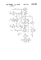
- FIG. 1 showing a block diagram of a typical prior art phase locked loop 10 having a binary phase shift key signal input at line 11.
- the signal on line 11 is applied to two mixers 12 and 13.
- the mixer 12 has a second input on line 14 from the voltage controlled oscillator which produces a down converted demodulated output signal on line 15 which is applied to a low pass filter 16.
- the output of low pass filter 16 on line 17 is applied to a hard limiter 18 to produce the desired data signals on output a line 19 which are applied to a prior art type analog multiplier 21 to produce the phase error signal (E S ) on line 22.
- This signal is applied to a low pass filter 23 which cleans up the error signal and controls the phase locked loop band width.
- the output of low pass filter 23 is applied as a voltage error signal on line 24 to the voltage control oscillator 25.
- the frequency output signal on line 26 from voltage controlled oscillator 25 is applied to a quadrature power splitter 27 to produce the an inphase signal on line 14 in the phase locked loop and to produce a 90° phase shifted quadrature signal on line 28 which is applied to the mixer 13 to produce a tracking error voltage signal on line 29.
- the error signal is applied to a low pass filter 31 which serves as a matched filter to maximize the signal to noise ratio on output line 32.
- the tracking error signal (E T ) is applied to the analog multiplier 21 to produce the aforementioned error signal E S on line 22 in the phase locked loop.
- a DC voltage must be applied to the VCO 25 in order to recover or acquire the incoming signal.
- a sweep circuit 33 produces a sweep voltage signal on line 34 which is applied to the summing circuit 35 to produce the corrected or supplemented error signal on line 24 to sweep the voltage control oscillator through the range of frequencies which encompasses the binary phase shift key signal on input line 11.
- a lock detector (not shown) is employed to disconnect the sweep voltage on line 34 from the summing circuit 35.
- Such prior art circuits are known to require excessive acquisition time because the phase lock loop band width is very narrow for low to medium data rate frequency receivers.
- FIG. 2 showing a simplified block diagram of the preferred embodiment of the present invention.
- the same BPSK input signal on line 11 is applied to identical mixers 12 and 13 which receive the aforementioned signals from input lines 14 and 28 as explained hereinbefore.
- the upper loop of phase locked loop 30 operates in the same manner as the prior art phased locked loops and the elements and lines are numbered the same as described hereinbefore.
- Sweep circuit 33' provides a sweep voltage signal on line 34' which is applied to a three input summing circuit 35' to produce an error signal on line 37 as an input to the voltage controlled oscillator.
- Sweep circuit 33' is not constrained in its sweep frequency by the phase locked loop band width as in phase locked loop 10 but may be swept at a very high speed until it reaches a predetermined plus or minus frequency error and is then disconnected from the summing circuit 35' by controls 38 to be explained in more detail hereinafter.
- the frequency detect and error generator 39 is connected into the automatic frequency lock loop as will be described in more detail hereinafter.
- the frequency error signal (V FE ) on line 41 is applied to the summing circuit 35' to produce a voltage frequency error signal that drives the phase locked loop 30 to a zero frequency error.
- the frequency detect and error generator 39 is disconnected from the automatic frequency lock loop so that the only input signal to the summing circuit 35' is the error signal on line 24 of the phase locked loop 30.
- the voltage controlled oscillator 25 is at the center frequency of the carrier so that the phase locked loop 30 does not have to compensate for any frequency error and can rapidly lock on to the phase of the carrier signal.
- the output of the low pass filter 31 on line 32 produces the aforementioned error tracking signal E T which is now applied to a hard limiter 43 and the phase lock detector 42.
- the output of the hard limiter 43 on line 44 is a hard limited error tracking signal (E T' ) that is applied to the phase lock detector.
- E T' hard limited error tracking signal
- the signal at the input of hard limiter 18 on line 17 and the output of hard limiter 18 on line 19 is applied to the phase lock detector 42.
- the input signals to frequency detect and error generator 39 are the aforementioned signals from the low pass filters 16 and 31 on line 17 and 32.
- the output of frequency detector 39 and phase lock detector 42 on lines 45 and 46 are couple to the aforementioned control 38.
- the sweep control circuit 33' When both signals on lines 45 and 46 indicate that neither the frequency detector 39 or the phase lock detector 42 are active, the sweep control circuit 33' is activated. Stated differently if either the frequency detector 39 or the phase lock detector 42 is active and attempting to lock the voltage controlled oscillator 25 onto the incoming signal then the sweep circuit 33' is deactivated. As will be explained in detail hereinafter the phase lock detector 42 preferably remains in the receiver circuit at all times.
- the frequency detector and error generator signal on line 41 is only active when the voltage control oscillator has reached a frequency that is very close to the center frequency and is predetermined to eliminate side band and false side band lock signals.
- the sweep circuit 33' may be operated in a very fast sweep mode until it reaches the window defined by the frequency detector and error generator 39, then the frequency detect and error generator may be operated very fast to drive the frequency of the phase lock loop 30 to zero frequency error. Because there is no overshoot, the phase lock loop may then be operated as a prior art phase lock loop to lock onto the phase discrepancy and not the frequency error.
- FIG. 3 showing a more detailed block diagram of the preferred embodiment invention.
- the numbers of the lines and elements in FIG. 3 which are identical to the elements and lines in FIG. 2 are numbered the same in FIG. 3 and do not require additional explanation herein.
- the mode of operation of the three sweep or lock circuits shown in FIG. 2 will now be explained.
- the aforementioned sweep control circuit 33' has an output line 34' which is connected to the aforementioned summing circuit 35+ through a switch or control 38'.
- the switch is operated by control signal line 47 at the output of NOR circuit 48.
- switch 38' When both input signals 45 and 46 from the frequency detect and phase detect circuits 39 and 44 respectively are absent, switch 38' is closed and the sweep control circuit 33' produces a sweep voltage signal on line 34' which causes the voltage control oscillator 25 to sweep through the frequency of the incoming signal on line 11. Before the voltage control oscillator 25 reaches the center frequency of the signal on line 11 it reaches the window or threshold set at high threshold line 49 and the low threshold line 51 at the frequency detector circuit 39.
- the signals before and after hard limiter 43 on lines 32 and 44 are applied to a second mixer 57 whose output on line 58 is applied as a negative input to subtractor 42' to produce a desired DC signal V L on line 59 indicative of whether the phase lock loop is properly locked or not.
- the threshold voltage input signal on line 61 to phase lock detector 42 is employed to assure that a true phase lock or high output signal is produced on line 59 indicative of a phase lock condition.
- the two input signals on lines 32 and 17 to the frequency detect error generator 39 in FIG. 2 are employed to derive the signal on line 53 shown as will now be explained.
- the before signal on line 17 is applied to a differentiating circuit 62 to produce a differentiated output signal on line 63 which is applied to a multiplier 64 which has a cross-coupled output signal from the output of hard limiter 43 on line 44.
- the signal on line 32 is applied to a differentiating circuit 65 whose output on line 66 is applied to a second multiplier 67 along with the cross-coupled output signal on line 19 from hard limiter 18.
- the output of multiplier 64 on line 17' is applied as a positive input to subtractor 68.
- the output of multiplier 67 on line 32' is applied as a negative input to subtractor 68 to produce the aforementioned voltage frequency error signal V FE on line 53.
- the voltage error signal on line 53 is applied via line 41 to the summing circuit 35'.
- the signal on line 53 is processed in the integrating circuit 54 which integrates all of the noise out of the voltage frequency error signal and by the process of integration produces the proper DC voltage signal on line 41 to correct the voltage controlled oscillator 25 so that the voltage frequency error signal on line 53 is driven to zero.
- the automatic frequency lock loop includes the output path signal on line 53 and the input DC signal path on line 41 and both branches of the phase lock loop therebetween. Thus, it will be understood that a major portion of the automatic frequency lock loop is superimposed on the phase lock loop and employ the same structure and signal lines which decreases the cost of the system.
- FIG. 4 showing a block diagram of a modification of the output detection circuits for the phase lock detector 42 and frequency detector 39.
- the output signals on line 56 and 57 to the subtractor 42' are unchanged.
- the cross-coupled signal from the output of the hard limiters 18 and 43 which are applied to the multiplier 67 and 64 respectively are now taken from the input side of the hard limiters 18 and 43 and applied to the multipliers 64 and 67.
- multiplier 64 has a line 32 input instead of the former line 44 input.
- multiplier 67 has a line 17 input instead of the former line 19 input.
- the multipliers 64 and 67 in the FIG. 4 embodiment must be analog multipliers which are expensive.
- the multipliers 64 and 67 in the FIG. 3 embodiment may be made inexpensively by employing the high speed electronic switch analog multipliers set forth in our co-pending application Ser. No. 07/222,699 filed 22 July 1988 for "A High Frequency Lock Detecting Circuit".
- the detecting circuits and multiplier shown in FIG. 4 employ true analog trigametric inputs which enable trigametric analysis of the signal. It can be shown that the signals on line 17 and 32 identified as V 1 and V 2 respectively are processed in the circuits shown to produce the following trigametric analysis that produces the output voltage frequency error signal V FE which is equal to W B where W B is the frequency difference between the incoming signal and the output signal on line 11 of the voltage control oscillator on line 26 as follows: ##EQU1##
- FIG. 5 showing a wave form diagram commonly referred to an S-curve of voltage frequency error at the output of the detector versus the frequency error between the input signal frequency and the frequency at the output of the VCO.
- the wave form 71 at a signal to noise ratio of 5 db represents the lowest signal to noise ratio at which it is desired to operate the present invention receiver.
- a 5 decibels signal to noise ratio is considered to be a very low value for BPSK receivers.
- the ability of the present invention to operate at this low signal to noise ratio without false lock on illustrates the desirability of the present invention.
- the wave forms 72 and 73 at signal to noise ratios of 10 and 20 decibels respectively will also operate at the same thresholds to be set for the frequency detector at the lower signal to noise ratio shown on wave form 71.
- the voltage peak for wave form 71 occurs at approximately 61/2 volts V FE in order to assure that the frequency detector is triggered under substantially all signal to noise operating conditions.
- a value of approximately 5 volts is set for the high threshold value TH H on line 49 as shown in FIG. 3.
- a value of the low threshold for the same S-curve which extends in the negative direction (not shown) is set at -5 volts on line 51. If the sweep is occurring from left to right the five volt threshold will first sense the point 75 on the signal to noise ratio curve 71.
- the present invention circuit shown in FIG. 3 can be made more cheaply than prior art circuits employing analog multipliers.
- the automatic frequency lock loop is both faster and more accurate than prior art circuits.
- the terminology smart sweep is applied to the automatic frequency lock loop circuit because the direction of sweep necessary to drive the frequency error to zero is sensed by the detection circuit so that sweeping circuits which repeat their sweep operations are no longer necessary. Under actual conditions it has been observed that the signal to noise ratios are much higher than the lower 5 decibel conditions set for the low threshold condition.
- the smart frequency sweep of the automatic frequency lock loop circuit usually takes over shortly after sweep has started or even before sweep is necessary and drives the center frequency to the frequency zero at point 76 shown on FIG. 5.
Landscapes
- Engineering & Computer Science (AREA)
- Computer Networks & Wireless Communication (AREA)
- Signal Processing (AREA)
- Stabilization Of Oscillater, Synchronisation, Frequency Synthesizers (AREA)
Abstract
Description
Claims (12)
Priority Applications (1)
| Application Number | Priority Date | Filing Date | Title |
|---|---|---|---|
| US07/263,677 US4916405A (en) | 1988-10-27 | 1988-10-27 | Smart sweep apparatus for data rate receivers |
Applications Claiming Priority (1)
| Application Number | Priority Date | Filing Date | Title |
|---|---|---|---|
| US07/263,677 US4916405A (en) | 1988-10-27 | 1988-10-27 | Smart sweep apparatus for data rate receivers |
Publications (1)
| Publication Number | Publication Date |
|---|---|
| US4916405A true US4916405A (en) | 1990-04-10 |
Family
ID=23002797
Family Applications (1)
| Application Number | Title | Priority Date | Filing Date |
|---|---|---|---|
| US07/263,677 Expired - Lifetime US4916405A (en) | 1988-10-27 | 1988-10-27 | Smart sweep apparatus for data rate receivers |
Country Status (1)
| Country | Link |
|---|---|
| US (1) | US4916405A (en) |
Cited By (13)
| Publication number | Priority date | Publication date | Assignee | Title |
|---|---|---|---|---|
| US5067139A (en) * | 1990-12-17 | 1991-11-19 | Motorola, Inc. | Coherent detector for QPSK modulation in a TDMA system |
| US5260671A (en) * | 1991-05-17 | 1993-11-09 | Hitachi, Ltd. | Receiving circuit for demodulating an angle modulated signal |
| US5287388A (en) * | 1991-06-25 | 1994-02-15 | Kabushiki Kaisha Toshiba | Frequency offset removal method and apparatus |
| US5396521A (en) * | 1992-10-19 | 1995-03-07 | Nec Corporation | Receiver capable of reducing power consumption in a PLL circuit |
| EP0739555A1 (en) * | 1994-01-14 | 1996-10-30 | Motorola, Inc. | Satellite receiver system having doppler frequency shift tracking |
| US5809096A (en) * | 1995-06-08 | 1998-09-15 | U.S. Philips Corporation | Digital transmission system comprising decision means for changing the synchronization mode |
| US5815535A (en) * | 1996-04-10 | 1998-09-29 | Samsung Electronics Co., Ltd. | Carrier recovery apparatus |
| US5832043A (en) * | 1995-04-03 | 1998-11-03 | Motorola, Inc. | System and method for maintaining continuous phase during up/down conversion of near-zero hertz intermediate frequencies |
| US6147560A (en) * | 1997-01-28 | 2000-11-14 | Telefonaktiebolget Lm Ericsson | Method and device relating to supervision and control of an oscillator signal |
| US6229864B1 (en) * | 1997-12-18 | 2001-05-08 | Philips Electronics North America Corporation | Phase locked loop lock condition detector |
| US6738429B1 (en) * | 1999-06-01 | 2004-05-18 | Harris Corporation | Decision-directed carrier frequency detector and method for QAM |
| EP1513310A1 (en) * | 2003-09-02 | 2005-03-09 | STMicroelectronics S.A. | Method and device for correcting the carrier frequency offset of a single carrier quadrature continuous modulated signal |
| US20050137815A1 (en) * | 2003-09-09 | 2005-06-23 | Quinlan Philip E. | Digital frequency measurement system and method with automatic frequency control |
Citations (2)
| Publication number | Priority date | Publication date | Assignee | Title |
|---|---|---|---|---|
| US4092606A (en) * | 1977-06-21 | 1978-05-30 | Lovelace Alan M Acting Adminis | Quadraphase demodulation |
| US4814719A (en) * | 1987-12-14 | 1989-03-21 | Ford Aerospace & Communications Corporation | Unsymmetrical QPSK demodulator |
-
1988
- 1988-10-27 US US07/263,677 patent/US4916405A/en not_active Expired - Lifetime
Patent Citations (2)
| Publication number | Priority date | Publication date | Assignee | Title |
|---|---|---|---|---|
| US4092606A (en) * | 1977-06-21 | 1978-05-30 | Lovelace Alan M Acting Adminis | Quadraphase demodulation |
| US4814719A (en) * | 1987-12-14 | 1989-03-21 | Ford Aerospace & Communications Corporation | Unsymmetrical QPSK demodulator |
Cited By (20)
| Publication number | Priority date | Publication date | Assignee | Title |
|---|---|---|---|---|
| US5067139A (en) * | 1990-12-17 | 1991-11-19 | Motorola, Inc. | Coherent detector for QPSK modulation in a TDMA system |
| US5260671A (en) * | 1991-05-17 | 1993-11-09 | Hitachi, Ltd. | Receiving circuit for demodulating an angle modulated signal |
| US5287388A (en) * | 1991-06-25 | 1994-02-15 | Kabushiki Kaisha Toshiba | Frequency offset removal method and apparatus |
| US5396521A (en) * | 1992-10-19 | 1995-03-07 | Nec Corporation | Receiver capable of reducing power consumption in a PLL circuit |
| AU664119B2 (en) * | 1992-10-19 | 1995-11-02 | Nec Corporation | Receiver capable of reducing power consumption in a PLL circuit |
| EP0739555A1 (en) * | 1994-01-14 | 1996-10-30 | Motorola, Inc. | Satellite receiver system having doppler frequency shift tracking |
| EP0739555A4 (en) * | 1994-01-14 | 1997-04-16 | Motorola Inc | Satellite receiver system having doppler frequency shift tracking |
| US5832043A (en) * | 1995-04-03 | 1998-11-03 | Motorola, Inc. | System and method for maintaining continuous phase during up/down conversion of near-zero hertz intermediate frequencies |
| US5809096A (en) * | 1995-06-08 | 1998-09-15 | U.S. Philips Corporation | Digital transmission system comprising decision means for changing the synchronization mode |
| US5815535A (en) * | 1996-04-10 | 1998-09-29 | Samsung Electronics Co., Ltd. | Carrier recovery apparatus |
| US6147560A (en) * | 1997-01-28 | 2000-11-14 | Telefonaktiebolget Lm Ericsson | Method and device relating to supervision and control of an oscillator signal |
| US6229864B1 (en) * | 1997-12-18 | 2001-05-08 | Philips Electronics North America Corporation | Phase locked loop lock condition detector |
| US6738429B1 (en) * | 1999-06-01 | 2004-05-18 | Harris Corporation | Decision-directed carrier frequency detector and method for QAM |
| EP1513310A1 (en) * | 2003-09-02 | 2005-03-09 | STMicroelectronics S.A. | Method and device for correcting the carrier frequency offset of a single carrier quadrature continuous modulated signal |
| US20050084052A1 (en) * | 2003-09-02 | 2005-04-21 | Stmicroelectronics S.A. | Method and device for processing the frequency shift of the carrier frequency of a signal modulated with a quadrature continuous single-carrier modulation |
| US7505543B2 (en) | 2003-09-02 | 2009-03-17 | Stmicroelectronics S.A. | Method and device for processing the frequency shift of the carrier frequency of a signal modulated with a quadrature continuous single-carrier modulation |
| US20090135979A1 (en) * | 2003-09-02 | 2009-05-28 | Bruno Paille | Method and device for processing the frequency shift of the carrier frequency of a signal modulated with a quadrature continuous single-carrier modulation |
| US8165259B2 (en) | 2003-09-02 | 2012-04-24 | Stmicroelectronics, S.A. | Method and device for processing the frequency shift of the carrier frequency of a signal modulated with a quadrature continuous single-carrier modulation |
| US20050137815A1 (en) * | 2003-09-09 | 2005-06-23 | Quinlan Philip E. | Digital frequency measurement system and method with automatic frequency control |
| US7352831B2 (en) * | 2003-09-09 | 2008-04-01 | Analog Devices, Inc. | Digital frequency measurement system and method with automatic frequency control |
Similar Documents
| Publication | Publication Date | Title |
|---|---|---|
| US4916405A (en) | Smart sweep apparatus for data rate receivers | |
| US4365211A (en) | Phase-locked loop with initialization loop | |
| US4349914A (en) | Bit synchronous switching system for space diversity operation | |
| US4596046A (en) | Split loop AFC system for a SSB receiver | |
| US5131014A (en) | Apparatus and method for recovery of multiphase modulated data | |
| US4423390A (en) | Side lock avoidance network for PSK demodulator | |
| US4092606A (en) | Quadraphase demodulation | |
| US4538280A (en) | Coherent spread spectrum pseudonoise tracking loop | |
| US3525945A (en) | System for reconstituting a carrier reference signal using a switchable phase lock loop | |
| US4316154A (en) | Automatic sweep and acquisition circuit for a phase locked loop | |
| US4354277A (en) | Signal acquisition system | |
| US4087628A (en) | Carrier lock detector | |
| US3983501A (en) | Hybrid tracking loop for detecting phase shift keyed signals | |
| US4561101A (en) | Clock-frequency recovery device adapted to high-frequency radiocommunications in disturbed media | |
| US4713630A (en) | BPSK Costas-type PLL circuit having false lock prevention | |
| US4625331A (en) | Automatic frequency control system or an SSB receiver | |
| US5022048A (en) | Programmable digital frequency-phase discriminator | |
| EP0373517B1 (en) | Digital automatic frequency control on pure sine waves | |
| US4569064A (en) | Device for recovery of clock frequency in digital transmission | |
| US3493866A (en) | Frequency stepped phase shift keyed communication system | |
| US4241454A (en) | Hard limiting acquisition technique for PSK carrier detector | |
| US4592077A (en) | NRZ digital data recovery | |
| US4636736A (en) | Variable phase signal demodulator | |
| US4901332A (en) | Noncoherent-coherent A.C. coupled base band AGC receiver | |
| US4811424A (en) | Rapid phase correcting carrier recovery circuit |
Legal Events
| Date | Code | Title | Description |
|---|---|---|---|
| AS | Assignment |
Owner name: UNISYS CORPORATION, TOWNSHIP LINE AND UNION MEETIN Free format text: ASSIGNMENT OF ASSIGNORS INTEREST.;ASSIGNORS:KEATE, CHRISTOPHER R.;THORNOCK, JEFFREY M.;WILLIAMS, BRUCE H.;REEL/FRAME:004970/0670 Effective date: 19881010 Owner name: UNISYS CORPORATION, PENNSYLVANIA Free format text: ASSIGNMENT OF ASSIGNORS INTEREST;ASSIGNORS:KEATE, CHRISTOPHER R.;THORNOCK, JEFFREY M.;WILLIAMS, BRUCE H.;REEL/FRAME:004970/0670 Effective date: 19881010 |
|
| STCF | Information on status: patent grant |
Free format text: PATENTED CASE |
|
| FEPP | Fee payment procedure |
Free format text: PAYOR NUMBER ASSIGNED (ORIGINAL EVENT CODE: ASPN); ENTITY STATUS OF PATENT OWNER: LARGE ENTITY |
|
| FPAY | Fee payment |
Year of fee payment: 4 |
|
| FPAY | Fee payment |
Year of fee payment: 8 |
|
| FPAY | Fee payment |
Year of fee payment: 12 |
|
| AS | Assignment |
Owner name: DEUTSCHE BANK TRUST COMPANY AMERICAS, AS COLLATERA Free format text: PATENT SECURITY AGREEMENT (PRIORITY LIEN);ASSIGNOR:UNISYS CORPORATION;REEL/FRAME:023355/0001 Effective date: 20090731 |
|
| AS | Assignment |
Owner name: DEUTSCHE BANK TRUST COMPANY AMERICAS, AS COLLATERA Free format text: PATENT SECURITY AGREEMENT (JUNIOR LIEN);ASSIGNOR:UNISYS CORPORATION;REEL/FRAME:023364/0098 Effective date: 20090731 |