US4901315A - Integrated data and timing circuitry for automatic circuit tester - Google Patents
Integrated data and timing circuitry for automatic circuit tester Download PDFInfo
- Publication number
- US4901315A US4901315A US07/177,067 US17706788A US4901315A US 4901315 A US4901315 A US 4901315A US 17706788 A US17706788 A US 17706788A US 4901315 A US4901315 A US 4901315A
- Authority
- US
- United States
- Prior art keywords
- memory
- edge
- trailing
- leading
- clock
- Prior art date
- Legal status (The legal status is an assumption and is not a legal conclusion. Google has not performed a legal analysis and makes no representation as to the accuracy of the status listed.)
- Expired - Lifetime
Links
- 230000015654 memory Effects 0.000 claims abstract description 60
- 238000012360 testing method Methods 0.000 claims abstract description 11
- 230000007704 transition Effects 0.000 claims abstract description 10
- 230000003111 delayed effect Effects 0.000 claims description 4
- 230000004044 response Effects 0.000 claims description 4
- 230000010363 phase shift Effects 0.000 abstract 1
- 230000008859 change Effects 0.000 description 6
- 239000013598 vector Substances 0.000 description 5
- 238000010586 diagram Methods 0.000 description 3
- 238000006243 chemical reaction Methods 0.000 description 1
- 230000001934 delay Effects 0.000 description 1
- 230000000694 effects Effects 0.000 description 1
- 230000006870 function Effects 0.000 description 1
- 238000000034 method Methods 0.000 description 1
- 230000008707 rearrangement Effects 0.000 description 1
Images

Classifications
-
- H—ELECTRICITY
- H03—ELECTRONIC CIRCUITRY
- H03K—PULSE TECHNIQUE
- H03K5/00—Manipulating of pulses not covered by one of the other main groups of this subclass
- H03K5/15—Arrangements in which pulses are delivered at different times at several outputs, i.e. pulse distributors
- H03K5/15013—Arrangements in which pulses are delivered at different times at several outputs, i.e. pulse distributors with more than two outputs
- H03K5/1502—Arrangements in which pulses are delivered at different times at several outputs, i.e. pulse distributors with more than two outputs programmable
-
- G—PHYSICS
- G01—MEASURING; TESTING
- G01R—MEASURING ELECTRIC VARIABLES; MEASURING MAGNETIC VARIABLES
- G01R31/00—Arrangements for testing electric properties; Arrangements for locating electric faults; Arrangements for electrical testing characterised by what is being tested not provided for elsewhere
- G01R31/28—Testing of electronic circuits, e.g. by signal tracer
- G01R31/317—Testing of digital circuits
- G01R31/3181—Functional testing
- G01R31/319—Tester hardware, i.e. output processing circuits
- G01R31/31917—Stimuli generation or application of test patterns to the device under test [DUT]
- G01R31/31919—Storing and outputting test patterns
-
- G—PHYSICS
- G01—MEASURING; TESTING
- G01R—MEASURING ELECTRIC VARIABLES; MEASURING MAGNETIC VARIABLES
- G01R31/00—Arrangements for testing electric properties; Arrangements for locating electric faults; Arrangements for electrical testing characterised by what is being tested not provided for elsewhere
- G01R31/28—Testing of electronic circuits, e.g. by signal tracer
- G01R31/317—Testing of digital circuits
- G01R31/3181—Functional testing
- G01R31/319—Tester hardware, i.e. output processing circuits
- G01R31/31917—Stimuli generation or application of test patterns to the device under test [DUT]
- G01R31/31928—Formatter
-
- G—PHYSICS
- G01—MEASURING; TESTING
- G01R—MEASURING ELECTRIC VARIABLES; MEASURING MAGNETIC VARIABLES
- G01R31/00—Arrangements for testing electric properties; Arrangements for locating electric faults; Arrangements for electrical testing characterised by what is being tested not provided for elsewhere
- G01R31/28—Testing of electronic circuits, e.g. by signal tracer
- G01R31/317—Testing of digital circuits
- G01R31/3181—Functional testing
- G01R31/319—Tester hardware, i.e. output processing circuits
- G01R31/3193—Tester hardware, i.e. output processing circuits with comparison between actual response and known fault free response
- G01R31/31935—Storing data, e.g. failure memory
Definitions
- the present invention is directed to automatic circuit testing and particularly to the data and timing circuits for such testers.
- the operation of automatic circuit testers can be thought of as the application, at some clock rate, of vectors to a group of nodes in a device under test.
- a "vector" is the ordered list of the binary values to be applied to all of the nodes within a clock period of the tester. Applied in this case can mean either impressing upon a node the particular binary value or testing the node for that value.
- There are very many performance criteria for automatic circuit testers but the major performance criteria are the number of nodes that a tester can test simultaneously and the speed at which it can apply vectors to those nodes. The latter criterion, namely, speed, is the one to which the present invention is directed.
- testers of conventional architecture have significant speed limitations. A large part of this limitation stems from the complexity exhibited by conventional tester architecture. Tester architectures differ, but the typical tester includes a large memory device for each tester terminal, or "pin.” Each location in the memory contains the data to be applied to the tester terminal at a different clock period.
- a formatter which translates the memory data either into signals applied to the tester pin (driving) or into comparisons made with the signals present on the tester pin (sensing).
- the pin electronics further requires timing information.
- the memories contain the data to be applied to the tester terminals within a given clock period, while the timing information indicates when, within a clock period, the data are to be applied.
- the formatter converts the data and the timing information into a signal of the proper value having the proper timing within a clock period.
- the circuitry for performing this conversion varies greatly from tester to tester, but it typically is fairly complex and includes counters, programmable delay lines, or combinations of these. At the high data rates required of modern testers, it is difficult to arrange all the circuitry so that various signals track each other accurately, and this difficulty increases with speed so as ultimately to place a limitation on the speed at which a tester can operate.
- I employ, for each channel, a leading-edge memory and a trailing-edge memory, which are clocked by respective individually delayed versions of a master clock signal. That is, I provide a programmable delay line for the leading-edge-memory clock signal and a separate programmable delay line for the trailing-edge-memory clock signal. I then apply signals to the tester terminals at times determined totally by the times of occurrence of the outputs of the leading-edge and trailing-edge memories. In this way, I employ no separate timing information, and the complexity required to combine data and timing information is eliminated.
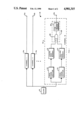
- FIG. l is a block diagram of the data/timing circuitry of a tester employing the teachings of the present invention.
- FIGS. 2A-2H represent a diagram depicting the contents of the leading-edge and trailing-edge memories and of the tester-terminal signals that result.
- FIG. 1 depicts a portion of an automatic circuit tester 10.
- the tester 10 is a device for driving or sensing circuit nodes connected to a multiplicity of tester pins such as pins 12a, 12b, and 12c of FIG. 1.
- the information for driving or sensing the pins is applied to them through channels 14a, 14b, and 14c in response to timing signals provided by a common master clock 16.
- clock 16 is a synthesized-frequency device, which generates a selectable high frequency. Such circuits enable the clock frequency to be chosen with a high resolution.
- Each channel includes a leading-edge memory 18 and a trailing-edge memory 20, which receive individual clock signals consisting of individually phase-shifted versions of the master clock signal produced by clock 16.
- delay lines in the forms of programmable phase shifters 22 and 24 are provided for the leading-edge and trailing-edge memories 18 and 20, respectively.
- the outputs of the leading-edge and trailing-edge memories are applied to a simple formatter 26, which transforms the memoryoutputs with no further timing adjustment to drive or sense signals at terminal 12c.
- the formatter is depicted as an exclusive-OR (XOR) gate 28 and a pin driver/sensor 30.
- the XOR gate receives as inputs the outputs of memories 18 and 20 and applies its own output to the pin driver/sensor 30.
- the driver/sensor 30 act in either a driver mode or a sensor mode. When it is in its driver mode, it merely drives the node connected to terminal 12c with one of two programmed levels in accordance with the binary output of the XOR gate 28. In the sensor mode, the driver/sensor 30 compares the signal on terminal 12c with a level determined by the binary output of XORgate 28 and transmits the result of the comparison to test-system circuitrynot shown in the drawings. For the remainder of the description, it will beassumed that driver/sensor 30 is operating in its driver mode.
- leading-edge memory 18 and trailing-edge memory 20 contain not only the data information but also, with the aid of their respective phase shifters22 and 24, the timing information required for tester operation. To understand this feature it is first necessary to recall conventional tester operation.
- a circuit tester for complex integrated circuits and circuit boards tests adevice under test ("DUT")--namely, a complex integrated circuit board--thatoperates with a basic DUT clock period. That is, in its normal operation, the signal at any DUT node does one of only three things: it changes its level once, or changes its level once and then returns to its initial level during one clock period, or does not change its level at all; no more activity than that occurs at any node during a single clock period.
- This clock period typically is established by a signal at a clock terminal, which signal may be the only exception to the foregoing rule.
- the conventional tester can be thought of conceptually as containing one bit of data per terminal per clock period. This is actually a simplification because, in addition to a single bit to indicatewhether the intended level is high or low, the tester typically also requires a further bit to cover the possibility that the node is to be presented with a high impedance in the driving mode or that the tester "doesn't care" what the signal is in the sensing mode. For present purposes, however, we will consider the conventional pin memory to includeonly a single bit for each terminal for each DUT period.
- a conventional tester In addition to the data information, a conventional tester also requires "time set" information, which defines the point within the DUT period at which the data should be applied.
- the time-set information is applied to the conventional-tester formatter along with the data information, and theformatter then applies the signal thus specified.
- the complexity of responding to this time-set information contributes to the speed limitations of conventional testers.
- the formatter 26 of the present invention receives only the signals from the leading-edge memory 18 and the trailing-edge memory 20; it does not receive separate signals that specify when, within the DUT clock period, the levels indicated by those signals are to be applied. Instead, the times at which the levels are applied are determined by the times of transitions in the outputs of memories 18 and 20.
- Timing of these transitions Two factors determine the timing of these transitions. The fine adjustment of this timing is made by the settings of programmable phase shifters 22 and 24. Within a signal burst--that is, within a sequence of vectors to beapplied at an uninterrupted DUT clock rate--the settings of the programmable phase shifters 22 and 24 are fixed, although they can be changed between bursts.
- the DUT is a 100-MHz chip; that is, the DUT period is 10 nsec.
- the tester clock 16 is set, not at 100 MHz, butrather at 1 GHz; that is, the tester clock period is 1 nsec. rather than 10nsec.
- the clock 16 will thus cause a new output from the leading-edge and trailing-edge memories 18 and 20 once every nanosecond.
- the access times of the actual memory chips that comprise leading-edge memory 18 and trailing-edge memory 20 are considerably longer than one nanosecond, but those skilled in the art will recognize that, by employingpipelining techniques, the effective access time for the memory circuits 18and 20 can be made to be one nanosecond if the order in which they are retrieved is predetermined.
- FIG. 2A depicts two DUT periods of the master clock signal.
- the positive-going zero crossings of the master clock define the beginning of one-nanosecond tester clock signals.
- phase shifter 22 In the absence of the phase shifters 22 and 24, the times at which new outputs from the leading-edge and trailing-edge memories 18 and 20 appear would coincide with the master-clock zero crossings. However, in the timing example depicted in FIGS. 2A-H, programmable phase shifter 22 is set to provide a 200-psec. delay, while phase shifter 24 is programmed to provide a 300-psec. delay. Consequently, the output of phase shifter 22 after hard limiting, depicted in FIG. 2B, is delayed from the zero crossings of the master clock signal in FIG. 2A.
- FIG. 2C lists the contents of the leading-edge-memory locations that determine the successive outputs caused by the low-to-high transitions of the individual clock signal depicted in FIG. 2B, and FIG. 2D depicts the resultant output of the leading-edge memory 18.
- FIG. 2E is a diagram similar to FIG. 2B but depicting the output of programmable phase shifter 24 rather than that of phase shifter 22.
- Phase shifter 24 is set for a delay of 300 psec. rather than the 200 psec. for which phase shifter 22 is programmed.
- FIGS. 2F and 2G depict the contents and outputs of trailing edge memory 22 just as FIGS. 2C and 2D depict those of the leading-edge memory 18.
- FIG. 2H depicts the output of XOR gate 28 in response to the outputs of theleading-edge memory 18 and trailing-edge memory 20, and it shows that the first pulse is 1.1 nsec. in duration and begins at 3.2 nsec. into the DUT period. That is, the leading edge is delayed from the beginning of the DUTperiod by 3.2 nsec. Of this 3.2 nsec., 0.2 nsec. results from the first phase shifter 22. The remaining 3.0 nsec. result from the fact that the leading-edge-memory values change after the first three entries, providing1.0 nsec. of delay per entry. That is, the first three entries in the leading-edge memory 18 are the same, namely, zeros, while the fourth and subsequent entries are ones.
- the pulse begins at the same time as it did in the first DUT period, but it lasts only 2.1 nanosecond rather than 1.1 nanosecond.
- the transition in the leading-edge-memory contents therefore occurs after the third entry for the second DUT period, just as it occurred after the third entry for the first DUT period, but the transition in the trailing-edge-memory contents occurs after the fifth location rather than after the fourth location, as it did for the first DUT period.
- the data information is contained, not in the individual memory contents, but in the relationship between those contents.
- the first illustrated output pulse isto be positive; that is, the signal starts at the low value, goes high, andthen returns to low.
- the contents of the leading- and trailing-edge memories are the same so that the result of theXOR function is a low value.
- a change in the trailing-edge output causes the two outputs to be different so that the XOR output goes high, and the subsequent change in the output of the trailing-edge memory causes the twooutputs to be the same again so that the XOR output returns to the low value.
- the output signal is again to begin at the low level, but the DUT period starts with the outputs of the two memories highrather than low, as they were at the beginning of the previous DUT period. This illustrates that it is not the individual values of the memory contents that determine the tester output; it is the comparison of their values.
- theformatter could include a flip-flop rather than an XOR gate.
- the simplicity of the XOR-gate arrangement is advantageous since it contributes to the simplicity that distinguishes this invention.
- the formatter arrangement is extremely simple; there is no complicated circuitry for applying timing information; the timing is simply determined by the time at which the data are retrieved from memory.
- the illustrated architecture greatly reduces the number of signals that must come from a central resource, since all address signals are generated in the individual pin electronics. This eliminates a major source of cross-talk. It also eliminates a large amount of "de-skewing" to insure that signals from a central resource all arrive at their respective destinations simultaneously.
- the clock is nearly the only signal that must be distributed from a central resource, and the clock is not required to reach all of the channels simultaneously; "de-skewing" is performed by the contents of the memories.
- This highly decentralized architecture also allows a system to be expanded simply; addition of channels does not dictate a great amount of re-arrangement of central circuitry.
- this architecture provides great time-set flexibility.
- the time within a given DUT period at which data are applied at a given pin is not in general the same as the data-application time at another pin for the same DUT period.
- the set of data-application times for all pins in the same DUTperiod is known as a time set, and conventional architectures, which set the time sets centrally, tend to restrict the number of different possibletime sets in a given vector burst.
- the present invention provides for a very large number of time sets when the DUT period is significantly longer than the shortest available tester clock period, and the data-application time can differ for every pin and every period if necessary.
- the present invention constitutes a significant advance in theart.
Landscapes
- Physics & Mathematics (AREA)
- Engineering & Computer Science (AREA)
- General Engineering & Computer Science (AREA)
- General Physics & Mathematics (AREA)
- Nonlinear Science (AREA)
- Tests Of Electronic Circuits (AREA)
Abstract
Description
Claims (2)
Applications Claiming Priority (1)
| Application Number | Priority Date | Filing Date | Title |
|---|---|---|---|
| GB8800303A GB2214314B (en) | 1988-01-07 | 1988-01-07 | Automatic circuit tester |
Publications (1)
| Publication Number | Publication Date |
|---|---|
| US4901315A true US4901315A (en) | 1990-02-13 |
Family
ID=10629619
Family Applications (1)
| Application Number | Title | Priority Date | Filing Date |
|---|---|---|---|
| US07/177,067 Expired - Lifetime US4901315A (en) | 1988-01-07 | 1988-04-04 | Integrated data and timing circuitry for automatic circuit tester |
Country Status (3)
| Country | Link |
|---|---|
| US (1) | US4901315A (en) |
| JP (1) | JPH02110387A (en) |
| GB (1) | GB2214314B (en) |
Cited By (1)
| Publication number | Priority date | Publication date | Assignee | Title |
|---|---|---|---|---|
| US5453993A (en) * | 1993-02-16 | 1995-09-26 | Mitsubishi Denki Kabushiki Kaisha | Semiconductor integrated circuit with clock selecting function |
Families Citing this family (2)
| Publication number | Priority date | Publication date | Assignee | Title |
|---|---|---|---|---|
| US5212443A (en) * | 1990-09-05 | 1993-05-18 | Schlumberger Technologies, Inc. | Event sequencer for automatic test equipment |
| CA2127192C (en) * | 1993-07-01 | 1999-09-07 | Alan Brent Hussey | Shaping ate bursts, particularly in gallium arsenide |
Citations (6)
| Publication number | Priority date | Publication date | Assignee | Title |
|---|---|---|---|---|
| US4450560A (en) * | 1981-10-09 | 1984-05-22 | Teradyne, Inc. | Tester for LSI devices and memory devices |
| US4451918A (en) * | 1981-10-09 | 1984-05-29 | Teradyne, Inc. | Test signal reloader |
| US4517661A (en) * | 1981-07-16 | 1985-05-14 | International Business Machines Corporation | Programmable chip tester having plural pin unit buffers which each store sufficient test data for independent operations by each pin unit |
| US4730318A (en) * | 1986-11-24 | 1988-03-08 | International Business Machines Corporation | Modular organized storage tester |
| US4788684A (en) * | 1985-09-09 | 1988-11-29 | Hitachi, Ltd. | Memory test apparatus |
| US4806852A (en) * | 1984-09-07 | 1989-02-21 | Megatest Corporation | Automatic test system with enhanced performance of timing generators |
-
1988
- 1988-01-07 GB GB8800303A patent/GB2214314B/en not_active Expired - Lifetime
- 1988-04-04 US US07/177,067 patent/US4901315A/en not_active Expired - Lifetime
-
1989
- 1989-01-06 JP JP64001121A patent/JPH02110387A/en active Pending
Patent Citations (6)
| Publication number | Priority date | Publication date | Assignee | Title |
|---|---|---|---|---|
| US4517661A (en) * | 1981-07-16 | 1985-05-14 | International Business Machines Corporation | Programmable chip tester having plural pin unit buffers which each store sufficient test data for independent operations by each pin unit |
| US4450560A (en) * | 1981-10-09 | 1984-05-22 | Teradyne, Inc. | Tester for LSI devices and memory devices |
| US4451918A (en) * | 1981-10-09 | 1984-05-29 | Teradyne, Inc. | Test signal reloader |
| US4806852A (en) * | 1984-09-07 | 1989-02-21 | Megatest Corporation | Automatic test system with enhanced performance of timing generators |
| US4788684A (en) * | 1985-09-09 | 1988-11-29 | Hitachi, Ltd. | Memory test apparatus |
| US4730318A (en) * | 1986-11-24 | 1988-03-08 | International Business Machines Corporation | Modular organized storage tester |
Cited By (1)
| Publication number | Priority date | Publication date | Assignee | Title |
|---|---|---|---|---|
| US5453993A (en) * | 1993-02-16 | 1995-09-26 | Mitsubishi Denki Kabushiki Kaisha | Semiconductor integrated circuit with clock selecting function |
Also Published As
| Publication number | Publication date |
|---|---|
| GB2214314A (en) | 1989-08-31 |
| JPH02110387A (en) | 1990-04-23 |
| GB2214314B (en) | 1992-01-02 |
| GB8800303D0 (en) | 1988-02-10 |
Similar Documents
| Publication | Publication Date | Title |
|---|---|---|
| US6243841B1 (en) | Automated test and evaluation sampling system and method | |
| US5212443A (en) | Event sequencer for automatic test equipment | |
| US4783785A (en) | Method and apparatus for diagnosis of logical circuits | |
| US4855615A (en) | Switching circuit avoiding glitches at the instant of switch-over between two clock signals | |
| EP0174409A1 (en) | Formatter for high speed test system | |
| US7398442B2 (en) | Electronic circuit with asynchronously operating components | |
| EP0600815A2 (en) | A high resolution programmable pulse generator | |
| EP0852730A1 (en) | Parallel processing integrated circuit tester | |
| US4635256A (en) | Formatter for high speed test system | |
| KR100389608B1 (en) | Timing Generator for Automatic Test Equipment Operating at High Data Rates | |
| US6771061B2 (en) | High speed tester with narrow output pulses | |
| US4789835A (en) | Control of signal timing apparatus in automatic test systems using minimal memory | |
| US4901315A (en) | Integrated data and timing circuitry for automatic circuit tester | |
| US5789958A (en) | Apparatus for controlling timing of signal pulses | |
| US5561691A (en) | Apparatus and method for data communication between two asynchronous buses | |
| US4599710A (en) | Integrated memory circuit of a series-parallel-series type | |
| US5293080A (en) | Method and apparatus for generating test waveforms to be applied to a device under test | |
| US5327076A (en) | Glitchless test signal generator | |
| US4270116A (en) | High speed data logical comparison device | |
| JPS5944648B2 (en) | Logical waveform generator | |
| JP2591849B2 (en) | Test circuit | |
| JP2897540B2 (en) | Semiconductor integrated circuit | |
| KR20010006850A (en) | Improved skew pointer generation | |
| JP3880811B2 (en) | Test equipment | |
| JPH03265214A (en) | Data delay device |
Legal Events
| Date | Code | Title | Description |
|---|---|---|---|
| AS | Assignment |
Owner name: GENRAD, LTD., MONMOUTH HOUSE, MONMOUTH ROAD, CHEAD Free format text: ASSIGNMENT OF ASSIGNORS INTEREST.;ASSIGNOR:HEAPS, WILLIAM I.;REEL/FRAME:004860/0187 Effective date: 19880314 Owner name: GENRAD, LTD., A BRITISH CORP., ENGLAND Free format text: ASSIGNMENT OF ASSIGNORS INTEREST;ASSIGNOR:HEAPS, WILLIAM I.;REEL/FRAME:004860/0187 Effective date: 19880314 |
|
| STCF | Information on status: patent grant |
Free format text: PATENTED CASE |
|
| FEPP | Fee payment procedure |
Free format text: PAYOR NUMBER ASSIGNED (ORIGINAL EVENT CODE: ASPN); ENTITY STATUS OF PATENT OWNER: LARGE ENTITY |
|
| FPAY | Fee payment |
Year of fee payment: 4 |
|
| FPAY | Fee payment |
Year of fee payment: 8 |
|
| SULP | Surcharge for late payment | ||
| REMI | Maintenance fee reminder mailed | ||
| AS | Assignment |
Owner name: FLEET NATIONAL BANK, AS AGENT, MASSACHUSETTS Free format text: PATENT COLLATERAL ASSIGNMENT AND SECURITY AGREEMENT;ASSIGNOR:GENRAD, INC.;REEL/FRAME:010731/0078 Effective date: 20000324 |
|
| FPAY | Fee payment |
Year of fee payment: 12 |
|
| AS | Assignment |
Owner name: GENRAD, INC., MASSACHUSETTS Free format text: ASSIGNMENT OF ASSIGNORS INTEREST;ASSIGNOR:BANK OF AMERICA;REEL/FRAME:019733/0312 Effective date: 20070731 |