US4901207A - Light emission element array and manufacturing method thereof - Google Patents
Light emission element array and manufacturing method thereof Download PDFInfo
- Publication number
- US4901207A US4901207A US07/204,502 US20450288A US4901207A US 4901207 A US4901207 A US 4901207A US 20450288 A US20450288 A US 20450288A US 4901207 A US4901207 A US 4901207A
- Authority
- US
- United States
- Prior art keywords
- light emission
- emission element
- light
- rod
- element array
- Prior art date
- Legal status (The legal status is an assumption and is not a legal conclusion. Google has not performed a legal analysis and makes no representation as to the accuracy of the status listed.)
- Expired - Lifetime
Links
Images
Classifications
-
- H—ELECTRICITY
- H01—ELECTRIC ELEMENTS
- H01L—SEMICONDUCTOR DEVICES NOT COVERED BY CLASS H10
- H01L33/00—Semiconductor devices with at least one potential-jump barrier or surface barrier specially adapted for light emission; Processes or apparatus specially adapted for the manufacture or treatment thereof or of parts thereof; Details thereof
-
- H—ELECTRICITY
- H04—ELECTRIC COMMUNICATION TECHNIQUE
- H04N—PICTORIAL COMMUNICATION, e.g. TELEVISION
- H04N1/00—Scanning, transmission or reproduction of documents or the like, e.g. facsimile transmission; Details thereof
- H04N1/024—Details of scanning heads ; Means for illuminating the original
- H04N1/028—Details of scanning heads ; Means for illuminating the original for picture information pick-up
- H04N1/02815—Means for illuminating the original, not specific to a particular type of pick-up head
-
- B—PERFORMING OPERATIONS; TRANSPORTING
- B41—PRINTING; LINING MACHINES; TYPEWRITERS; STAMPS
- B41J—TYPEWRITERS; SELECTIVE PRINTING MECHANISMS, i.e. MECHANISMS PRINTING OTHERWISE THAN FROM A FORME; CORRECTION OF TYPOGRAPHICAL ERRORS
- B41J2/00—Typewriters or selective printing mechanisms characterised by the printing or marking process for which they are designed
- B41J2/435—Typewriters or selective printing mechanisms characterised by the printing or marking process for which they are designed characterised by selective application of radiation to a printing material or impression-transfer material
- B41J2/447—Typewriters or selective printing mechanisms characterised by the printing or marking process for which they are designed characterised by selective application of radiation to a printing material or impression-transfer material using arrays of radiation sources
- B41J2/45—Typewriters or selective printing mechanisms characterised by the printing or marking process for which they are designed characterised by selective application of radiation to a printing material or impression-transfer material using arrays of radiation sources using light-emitting diode [LED] or laser arrays
-
- H—ELECTRICITY
- H04—ELECTRIC COMMUNICATION TECHNIQUE
- H04N—PICTORIAL COMMUNICATION, e.g. TELEVISION
- H04N1/00—Scanning, transmission or reproduction of documents or the like, e.g. facsimile transmission; Details thereof
- H04N1/024—Details of scanning heads ; Means for illuminating the original
- H04N1/028—Details of scanning heads ; Means for illuminating the original for picture information pick-up
- H04N1/02815—Means for illuminating the original, not specific to a particular type of pick-up head
- H04N1/02845—Means for illuminating the original, not specific to a particular type of pick-up head using an elongated light source, e.g. tubular lamp, LED array
- H04N1/02865—Means for illuminating the original, not specific to a particular type of pick-up head using an elongated light source, e.g. tubular lamp, LED array using an array of light sources or a combination of such arrays, e.g. an LED bar
-
- H—ELECTRICITY
- H04—ELECTRIC COMMUNICATION TECHNIQUE
- H04N—PICTORIAL COMMUNICATION, e.g. TELEVISION
- H04N1/00—Scanning, transmission or reproduction of documents or the like, e.g. facsimile transmission; Details thereof
- H04N1/024—Details of scanning heads ; Means for illuminating the original
- H04N1/028—Details of scanning heads ; Means for illuminating the original for picture information pick-up
- H04N1/02815—Means for illuminating the original, not specific to a particular type of pick-up head
- H04N1/02885—Means for compensating spatially uneven illumination, e.g. an aperture arrangement
- H04N1/0289—Light diffusing elements, e.g. plates or filters
-
- F—MECHANICAL ENGINEERING; LIGHTING; HEATING; WEAPONS; BLASTING
- F21—LIGHTING
- F21V—FUNCTIONAL FEATURES OR DETAILS OF LIGHTING DEVICES OR SYSTEMS THEREOF; STRUCTURAL COMBINATIONS OF LIGHTING DEVICES WITH OTHER ARTICLES, NOT OTHERWISE PROVIDED FOR
- F21V2200/00—Use of light guides, e.g. fibre optic devices, in lighting devices or systems
- F21V2200/20—Use of light guides, e.g. fibre optic devices, in lighting devices or systems of light guides of a generally planar shape
-
- F—MECHANICAL ENGINEERING; LIGHTING; HEATING; WEAPONS; BLASTING
- F21—LIGHTING
- F21V—FUNCTIONAL FEATURES OR DETAILS OF LIGHTING DEVICES OR SYSTEMS THEREOF; STRUCTURAL COMBINATIONS OF LIGHTING DEVICES WITH OTHER ARTICLES, NOT OTHERWISE PROVIDED FOR
- F21V5/00—Refractors for light sources
- F21V5/04—Refractors for light sources of lens shape
- F21V5/043—Refractors for light sources of lens shape the lens having cylindrical faces, e.g. rod lenses, toric lenses
-
- F—MECHANICAL ENGINEERING; LIGHTING; HEATING; WEAPONS; BLASTING
- F21—LIGHTING
- F21W—INDEXING SCHEME ASSOCIATED WITH SUBCLASSES F21K, F21L, F21S and F21V, RELATING TO USES OR APPLICATIONS OF LIGHTING DEVICES OR SYSTEMS
- F21W2111/00—Use or application of lighting devices or systems for signalling, marking or indicating, not provided for in codes F21W2102/00 – F21W2107/00
-
- F—MECHANICAL ENGINEERING; LIGHTING; HEATING; WEAPONS; BLASTING
- F21—LIGHTING
- F21Y—INDEXING SCHEME ASSOCIATED WITH SUBCLASSES F21K, F21L, F21S and F21V, RELATING TO THE FORM OR THE KIND OF THE LIGHT SOURCES OR OF THE COLOUR OF THE LIGHT EMITTED
- F21Y2115/00—Light-generating elements of semiconductor light sources
- F21Y2115/10—Light-emitting diodes [LED]
-
- G—PHYSICS
- G02—OPTICS
- G02B—OPTICAL ELEMENTS, SYSTEMS OR APPARATUS
- G02B6/00—Light guides; Structural details of arrangements comprising light guides and other optical elements, e.g. couplings
- G02B6/0001—Light guides; Structural details of arrangements comprising light guides and other optical elements, e.g. couplings specially adapted for lighting devices or systems
-
- H—ELECTRICITY
- H01—ELECTRIC ELEMENTS
- H01L—SEMICONDUCTOR DEVICES NOT COVERED BY CLASS H10
- H01L25/00—Assemblies consisting of a plurality of individual semiconductor or other solid state devices ; Multistep manufacturing processes thereof
- H01L25/03—Assemblies consisting of a plurality of individual semiconductor or other solid state devices ; Multistep manufacturing processes thereof all the devices being of a type provided for in the same subgroup of groups H01L27/00 - H01L33/00, or in a single subclass of H10K, H10N, e.g. assemblies of rectifier diodes
- H01L25/04—Assemblies consisting of a plurality of individual semiconductor or other solid state devices ; Multistep manufacturing processes thereof all the devices being of a type provided for in the same subgroup of groups H01L27/00 - H01L33/00, or in a single subclass of H10K, H10N, e.g. assemblies of rectifier diodes the devices not having separate containers
- H01L25/075—Assemblies consisting of a plurality of individual semiconductor or other solid state devices ; Multistep manufacturing processes thereof all the devices being of a type provided for in the same subgroup of groups H01L27/00 - H01L33/00, or in a single subclass of H10K, H10N, e.g. assemblies of rectifier diodes the devices not having separate containers the devices being of a type provided for in group H01L33/00
- H01L25/0753—Assemblies consisting of a plurality of individual semiconductor or other solid state devices ; Multistep manufacturing processes thereof all the devices being of a type provided for in the same subgroup of groups H01L27/00 - H01L33/00, or in a single subclass of H10K, H10N, e.g. assemblies of rectifier diodes the devices not having separate containers the devices being of a type provided for in group H01L33/00 the devices being arranged next to each other
-
- H—ELECTRICITY
- H01—ELECTRIC ELEMENTS
- H01L—SEMICONDUCTOR DEVICES NOT COVERED BY CLASS H10
- H01L2924/00—Indexing scheme for arrangements or methods for connecting or disconnecting semiconductor or solid-state bodies as covered by H01L24/00
- H01L2924/0001—Technical content checked by a classifier
- H01L2924/0002—Not covered by any one of groups H01L24/00, H01L24/00 and H01L2224/00
-
- H—ELECTRICITY
- H01—ELECTRIC ELEMENTS
- H01L—SEMICONDUCTOR DEVICES NOT COVERED BY CLASS H10
- H01L33/00—Semiconductor devices with at least one potential-jump barrier or surface barrier specially adapted for light emission; Processes or apparatus specially adapted for the manufacture or treatment thereof or of parts thereof; Details thereof
- H01L33/48—Semiconductor devices with at least one potential-jump barrier or surface barrier specially adapted for light emission; Processes or apparatus specially adapted for the manufacture or treatment thereof or of parts thereof; Details thereof characterised by the semiconductor body packages
- H01L33/58—Optical field-shaping elements
-
- H—ELECTRICITY
- H04—ELECTRIC COMMUNICATION TECHNIQUE
- H04N—PICTORIAL COMMUNICATION, e.g. TELEVISION
- H04N2201/00—Indexing scheme relating to scanning, transmission or reproduction of documents or the like, and to details thereof
- H04N2201/024—Indexing scheme relating to scanning, transmission or reproduction of documents or the like, and to details thereof deleted
- H04N2201/02487—Manufacturing details
-
- Y—GENERAL TAGGING OF NEW TECHNOLOGICAL DEVELOPMENTS; GENERAL TAGGING OF CROSS-SECTIONAL TECHNOLOGIES SPANNING OVER SEVERAL SECTIONS OF THE IPC; TECHNICAL SUBJECTS COVERED BY FORMER USPC CROSS-REFERENCE ART COLLECTIONS [XRACs] AND DIGESTS
- Y10—TECHNICAL SUBJECTS COVERED BY FORMER USPC
- Y10S—TECHNICAL SUBJECTS COVERED BY FORMER USPC CROSS-REFERENCE ART COLLECTIONS [XRACs] AND DIGESTS
- Y10S359/00—Optical: systems and elements
- Y10S359/90—Methods
-
- Y—GENERAL TAGGING OF NEW TECHNOLOGICAL DEVELOPMENTS; GENERAL TAGGING OF CROSS-SECTIONAL TECHNOLOGIES SPANNING OVER SEVERAL SECTIONS OF THE IPC; TECHNICAL SUBJECTS COVERED BY FORMER USPC CROSS-REFERENCE ART COLLECTIONS [XRACs] AND DIGESTS
- Y10—TECHNICAL SUBJECTS COVERED BY FORMER USPC
- Y10S—TECHNICAL SUBJECTS COVERED BY FORMER USPC CROSS-REFERENCE ART COLLECTIONS [XRACs] AND DIGESTS
- Y10S362/00—Illumination
- Y10S362/80—Light emitting diode
Definitions
- This invention relates to a light emission element array particularly used for a light source of an image sensor and also relates to a method of manufacturing the light emission element array of this character.
- an image information is read out by inducing a light from a light source on a surface of a material such as an original or an object to be inspected and by carrying out a photoelectric conversion of a light reflected from the surface of the original, for example, by using a linear image sensor.
- a light emitting diode element (called hereinafter LED) has been widely used as the light source described above for the reason that the LED is excellent in the reliability and long life time.
- the LED of single element emits a small amount of light having a short light reaching distance, so that a LED array in which a plurality of LEDs are linearly arranged is generally utilized.
- a known type of a LED array of this character comprises a row of LEDs and a columnar light converging lens unit arranged in parallel to the LED row to linearly converge the light on a predetermined position.
- the LED array having such structure or arrangement is liable to be varied in the light converging position because of certain reasons on the manufacture or usage thereof, and in particular, in case the LED array is utilized for an original read-out section of a copying machine, for example, the light converging position is liable not too often coincide with the original read-out position. This may cause a problem of unevenness of an output level from the read-out section even if the original with uniform reflection factor could be read because of unevenness of illumination at a portion of a read-out line or lowering of the entire illumination.
- the processing of a signal having such uneven output level will require a complexed signal processing circuit, and even if the complexed signal processing circuit is used, an improved signal to noise ratio (S/N) has not been expected.
- an object of this invention is to provide a light emission element array capable of substantially reducing the variation of illumination on the light converging position even if positional displacement or shifting of a constructional element is caused in usage or manufacture thereof.
- Another object of this invention is to provide a method of manufacturing a light emission element array capable of substantially eliminating the variation of the illumination on the light converging position.
- a light emission element array comprising a substrate, a plurality of light emission elements arranged linearly in a row on the substrate, and a rod like light converging lens unit arranged above the light emission element row in parallel thereto and adapted to diffuse and simultaneously converge transmitted light.
- the transmitted light is diffused and converged by arranging the light converging lens unit above the light emission element array, the distribution of illumination in the space above the light emission element array is made equalized. Accordingly, the lowering of the illumination at the read-out position can be substantially eliminated even in a case where the radiation difference of each light emission element and the misattachment of the respective elements of the array are generated or in a case where the light converging position does not coincide with the read-out position in the practical usage.
- a method of manufacturing the light emission element array comprising the steps of arranging linearly a plurality of light emission elements on a substrate to form a light emissing element row, roughening a surface of a rod like lens unit, and arranging the rod like lens unit having an outer surface roughened above the light emission element row so that the central axis of the rod like lens unit is in parallel to the central line of the light emission element row.
- a method of manufacturing a light emission element array comprising the steps of arranging linearly a plurality of light emission elements on a substrate to form a light emission element row, preparing a rod like lens unit by molding a mixture material of a lens material and light scattering particles contained therein, and arranging the thus prepared rod like lens unit above the light emission element row so that the central axis of the rod like lens unit is in parallel to the central line of the light emission element row.
- a light converging lens unit prepared by providing a roughened surface or formed by molding materials with particles having indexes of refractions different from each other is arranged above the light emission element row, so that the light emission element array of the character described hereinbefore can be easily manufactured.
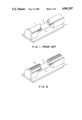
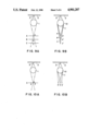
- FIG. 1 is a perspective view of a conventional light emission element array
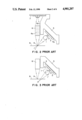
- FIG. 2 is an illustration of a front view of a close contact type image sensor to which the light emission element array shown in FIG. 1 is applied;
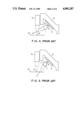
- FIGS. 3 to 6 are front views of image sensors of the type shown in FIG. 2 illustrative of the explanation of cases in which a light converging position does not accord with a read-out position;
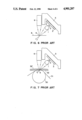
- FIG. 7 is a front view of an image sensor similar to that shown in FIG. 2 illustrative of the explanation of a case in which an original is bent in operation;
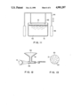
- FIG. 8 is a perspective view of a light emission element array according to this invention.
- FIGS. 9A, 9B, 10A and 10B are illustrations for the explanation of the operation of the light emission element array shown in FIG. 8;
- FIG. 11 shows a diagrammatical elevation of a device for carrying out a chemical treatment to a lens unit to form a roughened surface thereof;
- FIG. 12 is an illustration of an apparatus for carrying out a sandblast method to obtain a roughened surface of the lens unit.
- FIG. 13 is a cross sectional view of a rod like lens unit containing a material having an index of refraction different from that of the body of the lens unit.
- FIG. 1 shows a perspective view of one example of a light emitting diode (LED) array of conventional type
- a plurality of LEDs3 are linearly arranged in a row on a substrate 2
- a columnar or rod like light converging lens unit 1 for linearly converging the light from the LED array in a predetermined range is stationarily mounted on a lens supporting member 4 mounted on the substrate 2 adjacent to and in parallelto the LED row.
- FIG. 2 shows a sectional illustration of an original read-out section assembling the LED array shown in FIG. 1.
- a support member 5 is provided with an oblique surface 5a usually inclined at angles of about 40° to 45° with respect to a surface 8 of the original and a vertical surface 5b.
- the substrate 2 provided with the light converging lens unit 1and the LEDs 3 is mounted on the oblique surface 5a, and above the read-outposition 9 of the original surface 8 are arranged a linear image sensor 7 and an image focusing lens unit 6 which is secured to the vertical surface5b of the support member 5.
- the image focusing lens unit 6 is of a rod lensarray type comprising a plurality of rod lens elements 6a respectively having indexes of refractions gradually reducing from the central portion of the rod lens array towards the outer periphery thereof in such a manneras that light axes of the rod lens elements 6a are aligned in the vertical directions thereof to thereby focus the erected image having equal magnitude on a portion symmetric with a focus position with respect to thecentral position in the light axis directions of the image focusing lens unit 6.
- the image sensor 7 is of a close-contact type linear image sensor in which an image pick up element and an object to be picked up are made to correspond to each other at the ratio of 1:1 in the structural largeness.
- the light converging position of the LED array should significantly coincide with the original read-out position of the linear image sensor in order to ensure the illumination on the original surface required for the linear image sensor, and the positional relationship between these members or elements is adjusted to obtain the positional coincidence described above.
- FIG. 3 shows a case that the substrate 2 having the LED array is mounted onthe support member 5 in a shifted manner as denoted by reference numeral 2', and accordingly, the light collecting position of the LED array is also shifted and does not coincide with the original read-out position 9.
- FIG. 4 shows a case that the LED rows 3 are arranged in a shifted manner onthe substrate 2 as shown by reference numeral 3'.
- FIG. 5 shows a case that the position of the light converging lens unit 1 is shifted by warp thereof, for example, as designated by reference numeral 1'.
- FIG. 6 shows a case that the substrate 2 of the LED array is deformed such as warped or raised as denoted by reference numeral 2'.
- the light converging position does not coincide with the original read-out position and unevenness in the luminance will be caused on the original read-out position.
- FIG. 7 shows a case concerning the operation of an image scanner, in which the light from the light converging lens unit 1 is converged on the read-out position on a surface of a glass sheet 32 on which the original is mounted.
- FIG. 7 shows a case that when a platen roller 30 passes under the glass sheet 32, while pressing the lower surface of the glass, the glass sheet 32 is deformed or bent as shown by reference numeral 32' by the pressure of the platen roller 30 and the light converging position and the original read-out position are mutually shifted.
- FIG. 7 shows a case that the illumination on the original read-out position 9 is adversely influenced with the pressure of the platen roller 30.
- the light emission elements 3 comprising the light emitting diodes (LED) are linearly arranged on the substrate 2 as is stated with reference to FIG. 1, and a rod-like lens unit 10 made of a cylindrical columnar optical glass is mounted on the lens supporting member 4 above the light emission elements 3 in parallel thereto.
- the upper surface of the rod lens unit 10 is however provided with a roughened surface according to this invention so as to diffuse the emitting light. It will be sufficient for the roughened surface of the rod lens unit 10 to have such a degree of roughness as thatof a ground glass.
- FIGS. 9 and 10 are illustration for the explanation of the function of the light converging lens unit used for the LED array of this invention and adapted to diffuse and simultaneously converge the transmitted light.
- FIG. 9A the light emitted from the LED array 3 disposed on the substrate 2 is converged on a light receiving surface A by means of the rod lens unit 1 having a longitudinal columnar section.
- the intensities of the illuminations on the points a,b and c are substantially in inverse proportion to areas of the light receiving surfaces A, B and C illuminated by the light from the LEDs, so that the ratio of the maximum to the minimum intensities of illumination (variation) becomes more than several tens.
- FIG. 9B shows a case using the rod lens unit 10 accordingto this invention provided with the roughened outer light emitting surface as a light diffusing surface
- the illuminations on optional points a', b' and c' on the light receiving surfaces depend onsolid angles ⁇ , ⁇ and ⁇ constituted by tangential lines extending from the points a', b' and c' to the light diffusing surface of the rod lens unit 10, respectively and also depend on the luminances of the light diffusing surface.
- FIG. 10 is a set of illustrations for the explanation of the variation of the illuminations on the points a, d and e on the same reference surface A, and in a case shown in FIG. 10A of a conventional example, the light from the LED is not received at all on the points d and e, whereas in a case shown in FIG. 10B according to this invention, the points d' and e' face the light diffusing surface of the rod lens unit 10 with substantially the same solid angles as that with respect to the point a', so that the illuminations on these points a', d' and e' are all substantially equal to each other.
- FIGS. 11 and 12 are illustrations for the explanation of a method for forming a roughened surface on a rod lens unit according to this invention.
- FIG. 11 is a plan view of a device for effecting chemical treatment to the rod lens unit 10 to form the roughened surface thereof and the device comprises a treatment tank 51 filled with a treating liquid 52 including, for example, hydrofluoric acid of 10% and sulfuric acid of 10% and drive mechanisms 55 having such as hydraulic cylinder assemblies disposed on both sides of the tank 51.
- the drive mechanisms 55 serve to lower arm members 54 operatively connected to the mechanisms 55 to thereby dip the rod lens unit 10 supported by a holding member 53 connected at both ends to the arm members 54 in the treating liquid 52 contained in the tank 51, thus effecting the surface roughening to the rod lens unit 10.
- This treatment is performed at a temperature of 20° C. of the treating liquid for five minutes, for example.
- FIG. 12 is a plan view of a portion of a device for carrying out a sandblast method as another example for forming a roughened surface aroundthe outer peripheral surface of the rod lens unit 10.
- the sand 62 stored in a hopper 61 is supplied downwardly towards a blasting nozzle member 63 and the sand fallen into the nozzle member 63 is blasted against the outer peripheral surface of the rod lens unit 10 by a compressed air to make the surface rough.
- Metal particles (shots) such as iron or steel particles may be utilized as a material to be blasted instead of the sand.
- fine or micro particles such as glass may be adhered to the surface thereof.
- the surface roughening processes described above can be done to the entire outer peripheral surface of the rod lens unit 10, but the processes may beeffected to a certain portion, particularly the light emitting surface, by carrying out the masking process to the other portions.
- a rod lens unit may be constructed so that the light is diffused from the whole structure thereof.
- FIG. 13 shows a cross section of a rod lens unit of this character, which is made of an optical plastic resin 20 of cylindrical shape into which a number of glass beads, each having a diameter of about 3 ⁇ m and an index of refraction different from that of the plastic resin body 20, are uniformly distributed with the volumetric ratio of about 5%, and accordingly, the light transmitted therethrough is scattered inside the plastic rod lens unit to thereby create the light diffusion as a whole.
- the rod lens unit of the character described above can be manufactured by molding mixture material of the plastic resin and the glass beads into a mold cavity of a known injection molding machine.
- the rod like lens unitseach having a cylindrical configuration is not limited to the use of the lens unit of this shape and the other lens unit having such a semicircular or elliptical outer configuration can be utilized.
- the LED is referred to as a preferred light emission element, but according to the other preferred embodiment of this invention small light emitting sources arranged in a row may be adapted, and for example, a light emission element constituted by linearly arranging light fibers induced from a light source may be utilized for this invention.
Abstract
Description
Claims (18)
Applications Claiming Priority (2)
| Application Number | Priority Date | Filing Date | Title |
|---|---|---|---|
| JP62143687A JPH073891B2 (en) | 1987-06-09 | 1987-06-09 | Light emitting element array |
| JP62-143687 | 1987-06-09 |
Publications (1)
| Publication Number | Publication Date |
|---|---|
| US4901207A true US4901207A (en) | 1990-02-13 |
Family
ID=15344617
Family Applications (1)
| Application Number | Title | Priority Date | Filing Date |
|---|---|---|---|
| US07/204,502 Expired - Lifetime US4901207A (en) | 1987-06-09 | 1988-06-09 | Light emission element array and manufacturing method thereof |
Country Status (3)
| Country | Link |
|---|---|
| US (1) | US4901207A (en) |
| JP (1) | JPH073891B2 (en) |
| KR (1) | KR920001407B1 (en) |
Cited By (65)
| Publication number | Priority date | Publication date | Assignee | Title |
|---|---|---|---|---|
| US5032960A (en) * | 1989-02-15 | 1991-07-16 | Sharp Kabushiki Kaisha | Light source device with arrayed light emitting elements and manufacturing therefor |
| US5171429A (en) * | 1989-09-29 | 1992-12-15 | Inax Corporation | Apparatus for discharging water with passage selection sensor |
| US5187377A (en) * | 1988-07-15 | 1993-02-16 | Sharp Kabushiki Kaisha | LED array for emitting light of multiple wavelengths |
| US5400224A (en) * | 1993-01-08 | 1995-03-21 | Precision Lamp, Inc. | Lighting panel |
| US5836081A (en) * | 1996-05-29 | 1998-11-17 | Charles F. Schroeder | Light beam leveling means and method |
| US5969343A (en) * | 1995-08-24 | 1999-10-19 | Matsushita Electric Industrial Co., Ltd. | Linear illumination device |
| FR2782779A1 (en) * | 1998-05-15 | 2000-03-03 | Rohm Co Ltd | IMAGE READING DEVICE AND ILLUMINATING DEVICE USED FOR THE SAME |
| US6108965A (en) * | 1998-04-03 | 2000-08-29 | Brandenburg Limited | Trap for catching insects |
| US6268600B1 (en) | 1994-08-01 | 2001-07-31 | Matsushita Electric Industrial Co., Ltd. | Linear illumination device |
| US6271941B1 (en) | 1998-05-22 | 2001-08-07 | Eastman Kodak Company | Illuminant head assembly for a photographic film image scanner |
| US6305821B1 (en) * | 2000-02-08 | 2001-10-23 | Gen-Home Technology Co., Ltd. | Led lamp having ball-shaped light diffusing modifier |
| US20040012959A1 (en) * | 2002-07-17 | 2004-01-22 | Robertson Jones J. | LED replacement for fluorescent lighting |
| US20040057228A1 (en) * | 2002-09-19 | 2004-03-25 | Veutron Corporation | Light source of LED for scanner |
| US20040168359A1 (en) * | 2003-02-04 | 2004-09-02 | Cleaver Mark J. | Flexible illumination device for simulating neon lighting |
| US20040257665A1 (en) * | 2001-10-01 | 2004-12-23 | Fang Lei | Lens and method for producing a lens |
| US20070053182A1 (en) * | 2005-09-07 | 2007-03-08 | Jonas Robertson | Combination fluorescent and LED lighting system |
| US20070064409A1 (en) * | 2005-09-21 | 2007-03-22 | Ilight Technologies, Inc. | Elongated illumination device having uniform light intensity distribution |
| US20090046471A1 (en) * | 2007-07-09 | 2009-02-19 | Bruno Devos | Display panel with improved reflectivity |
| US20090109539A1 (en) * | 2007-07-09 | 2009-04-30 | Bruno Devos | Display panel with improved reflectivity |
| US20090161359A1 (en) * | 2007-12-21 | 2009-06-25 | Altair Engineering, Inc. | Light distribution using a light emitting diode assembly |
| US20090261706A1 (en) * | 2008-01-28 | 2009-10-22 | Eliot Sorella | LED Replacement Light Tube for Fluorescent Light Fixture |
| EP2128689A1 (en) * | 2008-05-27 | 2009-12-02 | Barco NV | A display panel with improved reflectivity |
| US20100008085A1 (en) * | 2008-07-09 | 2010-01-14 | Altair Engineering, Inc. | Method of forming led-based light and resulting led-based light |
| US20100027259A1 (en) * | 2008-07-31 | 2010-02-04 | Altair Engineering, Inc. | Fluorescent tube replacement having longitudinally oriented leds |
| US20100102730A1 (en) * | 2008-10-24 | 2010-04-29 | Altair Engineering, Inc. | Light and light sensor |
| US20100181925A1 (en) * | 2009-01-21 | 2010-07-22 | Altair Engineering, Inc. | Ballast/Line Detection Circuit for Fluorescent Replacement Lamps |
| US20100181933A1 (en) * | 2009-01-21 | 2010-07-22 | Altair Engineering, Inc. | Direct ac-to-dc converter for passive component minimization and universal operation of led arrays |
| US20100320922A1 (en) * | 2009-06-23 | 2010-12-23 | Altair Engineering, Inc. | Illumination device including leds and a switching power control system |
| US20110069486A1 (en) * | 2009-09-18 | 2011-03-24 | Martin John D | Lighting Arrangement Using LEDs |
| US7938562B2 (en) | 2008-10-24 | 2011-05-10 | Altair Engineering, Inc. | Lighting including integral communication apparatus |
| US20110234076A1 (en) * | 2010-03-26 | 2011-09-29 | Altair Engineering, Inc. | Inside-out led bulb |
| US8118447B2 (en) | 2007-12-20 | 2012-02-21 | Altair Engineering, Inc. | LED lighting apparatus with swivel connection |
| US8214084B2 (en) | 2008-10-24 | 2012-07-03 | Ilumisys, Inc. | Integration of LED lighting with building controls |
| US8256924B2 (en) | 2008-09-15 | 2012-09-04 | Ilumisys, Inc. | LED-based light having rapidly oscillating LEDs |
| US8299695B2 (en) | 2009-06-02 | 2012-10-30 | Ilumisys, Inc. | Screw-in LED bulb comprising a base having outwardly projecting nodes |
| CN102798030A (en) * | 2011-05-21 | 2012-11-28 | 辽宁奇辉电子系统工程有限公司 | Short-distance linear light source device based on linear array scanning camera |
| CN102798031A (en) * | 2011-05-21 | 2012-11-28 | 辽宁奇辉电子系统工程有限公司 | Long-distance linear light source device based on linear array scanning camera |
| CN102798041A (en) * | 2012-07-31 | 2012-11-28 | 大连鑫奇辉科技有限公司 | Spotlight with double lens for generating rectangular light spots |
| US8330381B2 (en) | 2009-05-14 | 2012-12-11 | Ilumisys, Inc. | Electronic circuit for DC conversion of fluorescent lighting ballast |
| US8360599B2 (en) | 2008-05-23 | 2013-01-29 | Ilumisys, Inc. | Electric shock resistant L.E.D. based light |
| US8444292B2 (en) | 2008-10-24 | 2013-05-21 | Ilumisys, Inc. | End cap substitute for LED-based tube replacement light |
| US8449142B1 (en) | 2009-10-14 | 2013-05-28 | C-M Glo, Llc | Reinforced housing structure for a lighted sign or lighting fixture |
| US8454193B2 (en) | 2010-07-08 | 2013-06-04 | Ilumisys, Inc. | Independent modules for LED fluorescent light tube replacement |
| US8523394B2 (en) | 2010-10-29 | 2013-09-03 | Ilumisys, Inc. | Mechanisms for reducing risk of shock during installation of light tube |
| US8541958B2 (en) | 2010-03-26 | 2013-09-24 | Ilumisys, Inc. | LED light with thermoelectric generator |
| US8556452B2 (en) | 2009-01-15 | 2013-10-15 | Ilumisys, Inc. | LED lens |
| US8596813B2 (en) | 2010-07-12 | 2013-12-03 | Ilumisys, Inc. | Circuit board mount for LED light tube |
| US8653984B2 (en) | 2008-10-24 | 2014-02-18 | Ilumisys, Inc. | Integration of LED lighting control with emergency notification systems |
| US8674626B2 (en) | 2008-09-02 | 2014-03-18 | Ilumisys, Inc. | LED lamp failure alerting system |
| US8866396B2 (en) | 2000-02-11 | 2014-10-21 | Ilumisys, Inc. | Light tube and power supply circuit |
| US8870415B2 (en) | 2010-12-09 | 2014-10-28 | Ilumisys, Inc. | LED fluorescent tube replacement light with reduced shock hazard |
| US8901823B2 (en) | 2008-10-24 | 2014-12-02 | Ilumisys, Inc. | Light and light sensor |
| WO2015000814A1 (en) * | 2013-07-02 | 2015-01-08 | Osram Opto Semiconductors Gmbh | Optoelectronic semiconductor device |
| US9057493B2 (en) | 2010-03-26 | 2015-06-16 | Ilumisys, Inc. | LED light tube with dual sided light distribution |
| US9072171B2 (en) | 2011-08-24 | 2015-06-30 | Ilumisys, Inc. | Circuit board mount for LED light |
| US9163794B2 (en) | 2012-07-06 | 2015-10-20 | Ilumisys, Inc. | Power supply assembly for LED-based light tube |
| US9184518B2 (en) | 2012-03-02 | 2015-11-10 | Ilumisys, Inc. | Electrical connector header for an LED-based light |
| US9271367B2 (en) | 2012-07-09 | 2016-02-23 | Ilumisys, Inc. | System and method for controlling operation of an LED-based light |
| US9267650B2 (en) | 2013-10-09 | 2016-02-23 | Ilumisys, Inc. | Lens for an LED-based light |
| US9285084B2 (en) | 2013-03-14 | 2016-03-15 | Ilumisys, Inc. | Diffusers for LED-based lights |
| US9510400B2 (en) | 2014-05-13 | 2016-11-29 | Ilumisys, Inc. | User input systems for an LED-based light |
| US9574717B2 (en) | 2014-01-22 | 2017-02-21 | Ilumisys, Inc. | LED-based light with addressed LEDs |
| US9909862B2 (en) | 2016-06-13 | 2018-03-06 | Google Llc | Curved array of light-emitting elements for sweeping out an angular range |
| US10161568B2 (en) | 2015-06-01 | 2018-12-25 | Ilumisys, Inc. | LED-based light with canted outer walls |
| US10212785B2 (en) | 2016-06-13 | 2019-02-19 | Google Llc | Staggered array of individually addressable light-emitting elements for sweeping out an angular range |
Families Citing this family (6)
| Publication number | Priority date | Publication date | Assignee | Title |
|---|---|---|---|---|
| JPH0470682U (en) * | 1990-10-26 | 1992-06-23 | ||
| JPH0496782U (en) * | 1991-01-31 | 1992-08-21 | ||
| JP2001085745A (en) * | 1999-09-14 | 2001-03-30 | Toshiba Corp | Light-emitting device |
| JP4902044B2 (en) * | 1999-09-24 | 2012-03-21 | シャープ株式会社 | Semiconductor laser device, optical transmission device, optical transmission system, electronic device, control device, connection connector, communication device, optical transmission method, and data transmission / reception method |
| JP2006310414A (en) * | 2005-04-27 | 2006-11-09 | Shimatec:Kk | Led lighting apparatus |
| CA2700108C (en) * | 2007-09-19 | 2015-10-13 | Mitsubishi Cable Industries, Ltd. | Optical fiber structure, system for fabricating the same, and block-like chip for use therein |
Citations (6)
| Publication number | Priority date | Publication date | Assignee | Title |
|---|---|---|---|---|
| US4330813A (en) * | 1979-12-07 | 1982-05-18 | Commissariat A L'energie Atomique | Illuminating device for large screen |
| US4630180A (en) * | 1984-06-11 | 1986-12-16 | Kabushiki Kaisha Toshiba | Light emitting diode array |
| US4691268A (en) * | 1985-10-21 | 1987-09-01 | Benson Walter L | Cast resin light-emitting display device |
| US4811507A (en) * | 1986-04-18 | 1989-03-14 | Blanchet Pierre A | Apparatus for the display of illuminated translucent documents |
| US4814667A (en) * | 1986-04-17 | 1989-03-21 | Kabushiki Kaisha Toshiba | Light emitting diode array having uniform illuminance distribution |
| US4847734A (en) * | 1987-07-31 | 1989-07-11 | Sharp Kabushiki Kaisha | Light emitting element array |
Family Cites Families (3)
| Publication number | Priority date | Publication date | Assignee | Title |
|---|---|---|---|---|
| JPS5638878A (en) * | 1979-09-07 | 1981-04-14 | Nanbu Kogyo Kk | Light emitting body to outside of which resinous light emitting portion is attached |
| JPS5982276U (en) * | 1982-11-23 | 1984-06-02 | ロ−ム株式会社 | light emitting display device |
| JPS6121934A (en) * | 1984-07-10 | 1986-01-30 | Nippon Sheet Glass Co Ltd | Etching process of glass bar |
-
1987
- 1987-06-09 JP JP62143687A patent/JPH073891B2/en not_active Expired - Fee Related
-
1988
- 1988-06-09 KR KR1019880006879A patent/KR920001407B1/en not_active IP Right Cessation
- 1988-06-09 US US07/204,502 patent/US4901207A/en not_active Expired - Lifetime
Patent Citations (6)
| Publication number | Priority date | Publication date | Assignee | Title |
|---|---|---|---|---|
| US4330813A (en) * | 1979-12-07 | 1982-05-18 | Commissariat A L'energie Atomique | Illuminating device for large screen |
| US4630180A (en) * | 1984-06-11 | 1986-12-16 | Kabushiki Kaisha Toshiba | Light emitting diode array |
| US4691268A (en) * | 1985-10-21 | 1987-09-01 | Benson Walter L | Cast resin light-emitting display device |
| US4814667A (en) * | 1986-04-17 | 1989-03-21 | Kabushiki Kaisha Toshiba | Light emitting diode array having uniform illuminance distribution |
| US4811507A (en) * | 1986-04-18 | 1989-03-14 | Blanchet Pierre A | Apparatus for the display of illuminated translucent documents |
| US4847734A (en) * | 1987-07-31 | 1989-07-11 | Sharp Kabushiki Kaisha | Light emitting element array |
Non-Patent Citations (4)
| Title |
|---|
| H. Yamanaka et al., "Light Emitting Diode With Hemispherical Emitting Surface for Optical Fiber Communication", Shingaku Giho, ED 79-75 (1979). |
| H. Yamanaka et al., Light Emitting Diode With Hemispherical Emitting Surface for Optical Fiber Communication , Shingaku Giho, ED 79 75 (1979). * |
| Komiya et al., "A4 Sized Contact Type Image Sensor", Shingaku Giko, IE 80-72 (1980). |
| Komiya et al., A4 Sized Contact Type Image Sensor , Shingaku Giko, IE 80 72 (1980). * |
Cited By (134)
| Publication number | Priority date | Publication date | Assignee | Title |
|---|---|---|---|---|
| US5187377A (en) * | 1988-07-15 | 1993-02-16 | Sharp Kabushiki Kaisha | LED array for emitting light of multiple wavelengths |
| US5032960A (en) * | 1989-02-15 | 1991-07-16 | Sharp Kabushiki Kaisha | Light source device with arrayed light emitting elements and manufacturing therefor |
| US5171429A (en) * | 1989-09-29 | 1992-12-15 | Inax Corporation | Apparatus for discharging water with passage selection sensor |
| US5400224A (en) * | 1993-01-08 | 1995-03-21 | Precision Lamp, Inc. | Lighting panel |
| US6268600B1 (en) | 1994-08-01 | 2001-07-31 | Matsushita Electric Industrial Co., Ltd. | Linear illumination device |
| US6127675A (en) * | 1995-08-24 | 2000-10-03 | Matsushita Electric Industrial Co., Ltd. | Linear illumination device |
| US5969343A (en) * | 1995-08-24 | 1999-10-19 | Matsushita Electric Industrial Co., Ltd. | Linear illumination device |
| US6072171A (en) * | 1995-08-24 | 2000-06-06 | Matsushita Electric Industrial Co., Ltd. | Linear illumination device |
| US5836081A (en) * | 1996-05-29 | 1998-11-17 | Charles F. Schroeder | Light beam leveling means and method |
| US6108965A (en) * | 1998-04-03 | 2000-08-29 | Brandenburg Limited | Trap for catching insects |
| FR2782779A1 (en) * | 1998-05-15 | 2000-03-03 | Rohm Co Ltd | IMAGE READING DEVICE AND ILLUMINATING DEVICE USED FOR THE SAME |
| FR2817324A1 (en) * | 1998-05-15 | 2002-05-31 | Rohm Co Ltd | LIGHTING DEVICE |
| FR2817323A1 (en) * | 1998-05-15 | 2002-05-31 | Rohm Co Ltd | IMAGE READING DEVICE AND ILLUMINATED LIGHTING DEVICE THEREFOR |
| US6469808B1 (en) | 1998-05-15 | 2002-10-22 | Rohm Co., Ltd. | Image reading apparatus and illuminator used for the same |
| US6271941B1 (en) | 1998-05-22 | 2001-08-07 | Eastman Kodak Company | Illuminant head assembly for a photographic film image scanner |
| US6305821B1 (en) * | 2000-02-08 | 2001-10-23 | Gen-Home Technology Co., Ltd. | Led lamp having ball-shaped light diffusing modifier |
| US8866396B2 (en) | 2000-02-11 | 2014-10-21 | Ilumisys, Inc. | Light tube and power supply circuit |
| US9739428B1 (en) | 2000-02-11 | 2017-08-22 | Ilumisys, Inc. | Light tube and power supply circuit |
| US9759392B2 (en) | 2000-02-11 | 2017-09-12 | Ilumisys, Inc. | Light tube and power supply circuit |
| US10054270B2 (en) | 2000-02-11 | 2018-08-21 | Ilumisys, Inc. | Light tube and power supply circuit |
| US9803806B2 (en) | 2000-02-11 | 2017-10-31 | Ilumisys, Inc. | Light tube and power supply circuit |
| US9222626B1 (en) | 2000-02-11 | 2015-12-29 | Ilumisys, Inc. | Light tube and power supply circuit |
| US8870412B1 (en) | 2000-02-11 | 2014-10-28 | Ilumisys, Inc. | Light tube and power supply circuit |
| US9752736B2 (en) | 2000-02-11 | 2017-09-05 | Ilumisys, Inc. | Light tube and power supply circuit |
| US9746139B2 (en) | 2000-02-11 | 2017-08-29 | Ilumisys, Inc. | Light tube and power supply circuit |
| US9006990B1 (en) | 2000-02-11 | 2015-04-14 | Ilumisys, Inc. | Light tube and power supply circuit |
| US9970601B2 (en) | 2000-02-11 | 2018-05-15 | Ilumisys, Inc. | Light tube and power supply circuit |
| US10557593B2 (en) | 2000-02-11 | 2020-02-11 | Ilumisys, Inc. | Light tube and power supply circuit |
| US9006993B1 (en) | 2000-02-11 | 2015-04-14 | Ilumisys, Inc. | Light tube and power supply circuit |
| US9416923B1 (en) | 2000-02-11 | 2016-08-16 | Ilumisys, Inc. | Light tube and power supply circuit |
| US9777893B2 (en) | 2000-02-11 | 2017-10-03 | Ilumisys, Inc. | Light tube and power supply circuit |
| US6965715B2 (en) * | 2001-10-01 | 2005-11-15 | Karl Storz Gmbh & Co. Kg | Lens and method for producing a lens |
| US20040257665A1 (en) * | 2001-10-01 | 2004-12-23 | Fang Lei | Lens and method for producing a lens |
| US7114830B2 (en) | 2002-07-17 | 2006-10-03 | Plastic Inventions And Patents, Inc. | LED replacement for fluorescent lighting |
| US20040012959A1 (en) * | 2002-07-17 | 2004-01-22 | Robertson Jones J. | LED replacement for fluorescent lighting |
| US20050225979A1 (en) * | 2002-07-17 | 2005-10-13 | Robertson Jonas J | LED replacement for fluorescent lighting |
| US6860628B2 (en) | 2002-07-17 | 2005-03-01 | Jonas J. Robertson | LED replacement for fluorescent lighting |
| US20040057228A1 (en) * | 2002-09-19 | 2004-03-25 | Veutron Corporation | Light source of LED for scanner |
| US8322883B2 (en) * | 2003-02-04 | 2012-12-04 | Ilight Technologies, Inc. | Flexible illumination device for simulating neon lighting |
| US20040168359A1 (en) * | 2003-02-04 | 2004-09-02 | Cleaver Mark J. | Flexible illumination device for simulating neon lighting |
| US7249865B2 (en) | 2005-09-07 | 2007-07-31 | Plastic Inventions And Patents | Combination fluorescent and LED lighting system |
| US20070053182A1 (en) * | 2005-09-07 | 2007-03-08 | Jonas Robertson | Combination fluorescent and LED lighting system |
| US20070064409A1 (en) * | 2005-09-21 | 2007-03-22 | Ilight Technologies, Inc. | Elongated illumination device having uniform light intensity distribution |
| US20090109539A1 (en) * | 2007-07-09 | 2009-04-30 | Bruno Devos | Display panel with improved reflectivity |
| US20090046471A1 (en) * | 2007-07-09 | 2009-02-19 | Bruno Devos | Display panel with improved reflectivity |
| US8118447B2 (en) | 2007-12-20 | 2012-02-21 | Altair Engineering, Inc. | LED lighting apparatus with swivel connection |
| US8928025B2 (en) | 2007-12-20 | 2015-01-06 | Ilumisys, Inc. | LED lighting apparatus with swivel connection |
| US7926975B2 (en) | 2007-12-21 | 2011-04-19 | Altair Engineering, Inc. | Light distribution using a light emitting diode assembly |
| US20100172149A1 (en) * | 2007-12-21 | 2010-07-08 | Altair Engineering, Inc. | Light distribution using a light emitting diode assembly |
| US7712918B2 (en) | 2007-12-21 | 2010-05-11 | Altair Engineering , Inc. | Light distribution using a light emitting diode assembly |
| US20090161359A1 (en) * | 2007-12-21 | 2009-06-25 | Altair Engineering, Inc. | Light distribution using a light emitting diode assembly |
| US20090261706A1 (en) * | 2008-01-28 | 2009-10-22 | Eliot Sorella | LED Replacement Light Tube for Fluorescent Light Fixture |
| US8360599B2 (en) | 2008-05-23 | 2013-01-29 | Ilumisys, Inc. | Electric shock resistant L.E.D. based light |
| US8807785B2 (en) | 2008-05-23 | 2014-08-19 | Ilumisys, Inc. | Electric shock resistant L.E.D. based light |
| EP2128689A1 (en) * | 2008-05-27 | 2009-12-02 | Barco NV | A display panel with improved reflectivity |
| US7976196B2 (en) | 2008-07-09 | 2011-07-12 | Altair Engineering, Inc. | Method of forming LED-based light and resulting LED-based light |
| US20100008085A1 (en) * | 2008-07-09 | 2010-01-14 | Altair Engineering, Inc. | Method of forming led-based light and resulting led-based light |
| US20100027259A1 (en) * | 2008-07-31 | 2010-02-04 | Altair Engineering, Inc. | Fluorescent tube replacement having longitudinally oriented leds |
| US7946729B2 (en) | 2008-07-31 | 2011-05-24 | Altair Engineering, Inc. | Fluorescent tube replacement having longitudinally oriented LEDs |
| US8674626B2 (en) | 2008-09-02 | 2014-03-18 | Ilumisys, Inc. | LED lamp failure alerting system |
| US8256924B2 (en) | 2008-09-15 | 2012-09-04 | Ilumisys, Inc. | LED-based light having rapidly oscillating LEDs |
| US11333308B2 (en) | 2008-10-24 | 2022-05-17 | Ilumisys, Inc. | Light and light sensor |
| US20110188240A1 (en) * | 2008-10-24 | 2011-08-04 | Altair Engineering, Inc. | Lighting including integral communication apparatus |
| US20100102730A1 (en) * | 2008-10-24 | 2010-04-29 | Altair Engineering, Inc. | Light and light sensor |
| US10713915B2 (en) | 2008-10-24 | 2020-07-14 | Ilumisys, Inc. | Integration of LED lighting control with emergency notification systems |
| US10571115B2 (en) | 2008-10-24 | 2020-02-25 | Ilumisys, Inc. | Lighting including integral communication apparatus |
| US10560992B2 (en) | 2008-10-24 | 2020-02-11 | Ilumisys, Inc. | Light and light sensor |
| US11073275B2 (en) | 2008-10-24 | 2021-07-27 | Ilumisys, Inc. | Lighting including integral communication apparatus |
| US9398661B2 (en) | 2008-10-24 | 2016-07-19 | Ilumisys, Inc. | Light and light sensor |
| US8901823B2 (en) | 2008-10-24 | 2014-12-02 | Ilumisys, Inc. | Light and light sensor |
| US8653984B2 (en) | 2008-10-24 | 2014-02-18 | Ilumisys, Inc. | Integration of LED lighting control with emergency notification systems |
| US9353939B2 (en) | 2008-10-24 | 2016-05-31 | iLumisys, Inc | Lighting including integral communication apparatus |
| US9585216B2 (en) | 2008-10-24 | 2017-02-28 | Ilumisys, Inc. | Integration of LED lighting with building controls |
| US8324817B2 (en) | 2008-10-24 | 2012-12-04 | Ilumisys, Inc. | Light and light sensor |
| US10342086B2 (en) | 2008-10-24 | 2019-07-02 | Ilumisys, Inc. | Integration of LED lighting with building controls |
| US10932339B2 (en) | 2008-10-24 | 2021-02-23 | Ilumisys, Inc. | Light and light sensor |
| US10973094B2 (en) | 2008-10-24 | 2021-04-06 | Ilumisys, Inc. | Integration of LED lighting with building controls |
| US10182480B2 (en) | 2008-10-24 | 2019-01-15 | Ilumisys, Inc. | Light and light sensor |
| US10176689B2 (en) | 2008-10-24 | 2019-01-08 | Ilumisys, Inc. | Integration of led lighting control with emergency notification systems |
| US7938562B2 (en) | 2008-10-24 | 2011-05-10 | Altair Engineering, Inc. | Lighting including integral communication apparatus |
| US9635727B2 (en) | 2008-10-24 | 2017-04-25 | Ilumisys, Inc. | Light and light sensor |
| US8214084B2 (en) | 2008-10-24 | 2012-07-03 | Ilumisys, Inc. | Integration of LED lighting with building controls |
| US8946996B2 (en) | 2008-10-24 | 2015-02-03 | Ilumisys, Inc. | Light and light sensor |
| US8444292B2 (en) | 2008-10-24 | 2013-05-21 | Ilumisys, Inc. | End cap substitute for LED-based tube replacement light |
| US8251544B2 (en) | 2008-10-24 | 2012-08-28 | Ilumisys, Inc. | Lighting including integral communication apparatus |
| US10036549B2 (en) | 2008-10-24 | 2018-07-31 | Ilumisys, Inc. | Lighting including integral communication apparatus |
| US9101026B2 (en) | 2008-10-24 | 2015-08-04 | Ilumisys, Inc. | Integration of LED lighting with building controls |
| US8556452B2 (en) | 2009-01-15 | 2013-10-15 | Ilumisys, Inc. | LED lens |
| US20100181933A1 (en) * | 2009-01-21 | 2010-07-22 | Altair Engineering, Inc. | Direct ac-to-dc converter for passive component minimization and universal operation of led arrays |
| US20100181925A1 (en) * | 2009-01-21 | 2010-07-22 | Altair Engineering, Inc. | Ballast/Line Detection Circuit for Fluorescent Replacement Lamps |
| US8664880B2 (en) | 2009-01-21 | 2014-03-04 | Ilumisys, Inc. | Ballast/line detection circuit for fluorescent replacement lamps |
| US8362710B2 (en) | 2009-01-21 | 2013-01-29 | Ilumisys, Inc. | Direct AC-to-DC converter for passive component minimization and universal operation of LED arrays |
| US8330381B2 (en) | 2009-05-14 | 2012-12-11 | Ilumisys, Inc. | Electronic circuit for DC conversion of fluorescent lighting ballast |
| US8299695B2 (en) | 2009-06-02 | 2012-10-30 | Ilumisys, Inc. | Screw-in LED bulb comprising a base having outwardly projecting nodes |
| US8421366B2 (en) | 2009-06-23 | 2013-04-16 | Ilumisys, Inc. | Illumination device including LEDs and a switching power control system |
| US20100320922A1 (en) * | 2009-06-23 | 2010-12-23 | Altair Engineering, Inc. | Illumination device including leds and a switching power control system |
| US8449140B2 (en) | 2009-09-18 | 2013-05-28 | C-M Glo, Llc | Lighting arrangement using LEDs |
| US20110069486A1 (en) * | 2009-09-18 | 2011-03-24 | Martin John D | Lighting Arrangement Using LEDs |
| US8449142B1 (en) | 2009-10-14 | 2013-05-28 | C-M Glo, Llc | Reinforced housing structure for a lighted sign or lighting fixture |
| US8540401B2 (en) | 2010-03-26 | 2013-09-24 | Ilumisys, Inc. | LED bulb with internal heat dissipating structures |
| US8541958B2 (en) | 2010-03-26 | 2013-09-24 | Ilumisys, Inc. | LED light with thermoelectric generator |
| US20110234076A1 (en) * | 2010-03-26 | 2011-09-29 | Altair Engineering, Inc. | Inside-out led bulb |
| US9395075B2 (en) | 2010-03-26 | 2016-07-19 | Ilumisys, Inc. | LED bulb for incandescent bulb replacement with internal heat dissipating structures |
| US8840282B2 (en) | 2010-03-26 | 2014-09-23 | Ilumisys, Inc. | LED bulb with internal heat dissipating structures |
| US9013119B2 (en) | 2010-03-26 | 2015-04-21 | Ilumisys, Inc. | LED light with thermoelectric generator |
| US9057493B2 (en) | 2010-03-26 | 2015-06-16 | Ilumisys, Inc. | LED light tube with dual sided light distribution |
| US8454193B2 (en) | 2010-07-08 | 2013-06-04 | Ilumisys, Inc. | Independent modules for LED fluorescent light tube replacement |
| US8596813B2 (en) | 2010-07-12 | 2013-12-03 | Ilumisys, Inc. | Circuit board mount for LED light tube |
| US8523394B2 (en) | 2010-10-29 | 2013-09-03 | Ilumisys, Inc. | Mechanisms for reducing risk of shock during installation of light tube |
| US8894430B2 (en) | 2010-10-29 | 2014-11-25 | Ilumisys, Inc. | Mechanisms for reducing risk of shock during installation of light tube |
| US8870415B2 (en) | 2010-12-09 | 2014-10-28 | Ilumisys, Inc. | LED fluorescent tube replacement light with reduced shock hazard |
| CN102798031A (en) * | 2011-05-21 | 2012-11-28 | 辽宁奇辉电子系统工程有限公司 | Long-distance linear light source device based on linear array scanning camera |
| CN102798030A (en) * | 2011-05-21 | 2012-11-28 | 辽宁奇辉电子系统工程有限公司 | Short-distance linear light source device based on linear array scanning camera |
| US9072171B2 (en) | 2011-08-24 | 2015-06-30 | Ilumisys, Inc. | Circuit board mount for LED light |
| US9184518B2 (en) | 2012-03-02 | 2015-11-10 | Ilumisys, Inc. | Electrical connector header for an LED-based light |
| US9163794B2 (en) | 2012-07-06 | 2015-10-20 | Ilumisys, Inc. | Power supply assembly for LED-based light tube |
| US9807842B2 (en) | 2012-07-09 | 2017-10-31 | Ilumisys, Inc. | System and method for controlling operation of an LED-based light |
| US9271367B2 (en) | 2012-07-09 | 2016-02-23 | Ilumisys, Inc. | System and method for controlling operation of an LED-based light |
| US10278247B2 (en) | 2012-07-09 | 2019-04-30 | Ilumisys, Inc. | System and method for controlling operation of an LED-based light |
| US10966295B2 (en) | 2012-07-09 | 2021-03-30 | Ilumisys, Inc. | System and method for controlling operation of an LED-based light |
| CN102798041A (en) * | 2012-07-31 | 2012-11-28 | 大连鑫奇辉科技有限公司 | Spotlight with double lens for generating rectangular light spots |
| US9285084B2 (en) | 2013-03-14 | 2016-03-15 | Ilumisys, Inc. | Diffusers for LED-based lights |
| WO2015000814A1 (en) * | 2013-07-02 | 2015-01-08 | Osram Opto Semiconductors Gmbh | Optoelectronic semiconductor device |
| US9267650B2 (en) | 2013-10-09 | 2016-02-23 | Ilumisys, Inc. | Lens for an LED-based light |
| US9574717B2 (en) | 2014-01-22 | 2017-02-21 | Ilumisys, Inc. | LED-based light with addressed LEDs |
| US10260686B2 (en) | 2014-01-22 | 2019-04-16 | Ilumisys, Inc. | LED-based light with addressed LEDs |
| US9510400B2 (en) | 2014-05-13 | 2016-11-29 | Ilumisys, Inc. | User input systems for an LED-based light |
| US10690296B2 (en) | 2015-06-01 | 2020-06-23 | Ilumisys, Inc. | LED-based light with canted outer walls |
| US10161568B2 (en) | 2015-06-01 | 2018-12-25 | Ilumisys, Inc. | LED-based light with canted outer walls |
| US11028972B2 (en) | 2015-06-01 | 2021-06-08 | Ilumisys, Inc. | LED-based light with canted outer walls |
| US11428370B2 (en) | 2015-06-01 | 2022-08-30 | Ilumisys, Inc. | LED-based light with canted outer walls |
| US10598482B2 (en) | 2016-06-13 | 2020-03-24 | Google Llc | Curved array of light-emitting elements for sweeping out an angular range |
| US9909862B2 (en) | 2016-06-13 | 2018-03-06 | Google Llc | Curved array of light-emitting elements for sweeping out an angular range |
| US10212785B2 (en) | 2016-06-13 | 2019-02-19 | Google Llc | Staggered array of individually addressable light-emitting elements for sweeping out an angular range |
Also Published As
| Publication number | Publication date |
|---|---|
| JPS63307785A (en) | 1988-12-15 |
| KR890001406A (en) | 1989-03-20 |
| KR920001407B1 (en) | 1992-02-13 |
| JPH073891B2 (en) | 1995-01-18 |
Similar Documents
| Publication | Publication Date | Title |
|---|---|---|
| US4901207A (en) | Light emission element array and manufacturing method thereof | |
| US5775791A (en) | Surface emission apparatus | |
| US6981792B2 (en) | Backlight device and liquid crystal display device | |
| TWI296694B (en) | ||
| US4847734A (en) | Light emitting element array | |
| KR20120037503A (en) | Illumination optical system of image capturing device | |
| US4465938A (en) | Apparatus for detecting a particle agglutination pattern | |
| US20050248961A1 (en) | Resembling prismatic structure of light guide plate | |
| CN102003638A (en) | Light emitting apparatus, surface light source apparatus and display apparatus | |
| US7160016B2 (en) | Light guide plate with convergence concavities and method for manufacturing the light guide plate | |
| US20050045898A1 (en) | Light-emitting diode and backlight system using the same | |
| CN101398509A (en) | Light guide and image sensor module | |
| CN102182981A (en) | LED linear light source and reading apparatus | |
| JP2005301016A (en) | Light guide plate for backlight of liquid crystal display | |
| US4665036A (en) | Illuminating device for the optical, particularly image-analytical evaluation of microbiological objects | |
| FI74147C (en) | ANORDNING FOER OPTISK CONTROL AV OBJEKT. | |
| JPH09159831A (en) | Light transmission plate and its production | |
| CN1542466A (en) | Light conducting plate structure | |
| CN216647373U (en) | Two-dimensional code detection device | |
| CN114139562A (en) | Two-dimensional code detection device | |
| US20040136077A1 (en) | Light guide plate having diffusion dots with microlenses | |
| JPH06289393A (en) | Illuminator | |
| CN210269574U (en) | Accurate light emitting device for detection and measuring instrument | |
| JP4637732B2 (en) | Light guide plate and manufacturing method thereof | |
| US7786441B2 (en) | Tensiographic drophead |
Legal Events
| Date | Code | Title | Description |
|---|---|---|---|
| AS | Assignment |
Owner name: KABUSHIKI KAISHA TOSHIBA, 72, HORIKAWA-CHO, SAIWAI Free format text: ASSIGNMENT OF ASSIGNORS INTEREST.;ASSIGNORS:SATO, NAOKI;TSUTSUMI, TERUO;KATOH, MASAAKI;REEL/FRAME:004927/0571 Effective date: 19880718 Owner name: SHARP KABUSHIKI KAISHA, 22-22, NAGAIKE-CHO, ABENO- Free format text: ASSIGNMENT OF ASSIGNORS INTEREST.;ASSIGNORS:SATO, NAOKI;TSUTSUMI, TERUO;KATOH, MASAAKI;REEL/FRAME:004927/0571 Effective date: 19880718 Owner name: KABUSHIKI KAISHA TOSHIBA, JAPAN Free format text: ASSIGNMENT OF ASSIGNORS INTEREST;ASSIGNORS:SATO, NAOKI;TSUTSUMI, TERUO;KATOH, MASAAKI;REEL/FRAME:004927/0571 Effective date: 19880718 Owner name: SHARP KABUSHIKI KAISHA, JAPAN Free format text: ASSIGNMENT OF ASSIGNORS INTEREST;ASSIGNORS:SATO, NAOKI;TSUTSUMI, TERUO;KATOH, MASAAKI;REEL/FRAME:004927/0571 Effective date: 19880718 |
|
| STCF | Information on status: patent grant |
Free format text: PATENTED CASE |
|
| FPAY | Fee payment |
Year of fee payment: 4 |
|
| FPAY | Fee payment |
Year of fee payment: 8 |
|
| FPAY | Fee payment |
Year of fee payment: 12 |