US4901127A - Circuit including a combined insulated gate bipolar transistor/MOSFET - Google Patents
Circuit including a combined insulated gate bipolar transistor/MOSFET Download PDFInfo
- Publication number
- US4901127A US4901127A US07/254,897 US25489788A US4901127A US 4901127 A US4901127 A US 4901127A US 25489788 A US25489788 A US 25489788A US 4901127 A US4901127 A US 4901127A
- Authority
- US
- United States
- Prior art keywords
- region
- major surface
- drain
- collector
- drift
- Prior art date
- Legal status (The legal status is an assumption and is not a legal conclusion. Google has not performed a legal analysis and makes no representation as to the accuracy of the status listed.)
- Expired - Lifetime
Links
Images

Classifications
-
- H—ELECTRICITY
- H10—SEMICONDUCTOR DEVICES; ELECTRIC SOLID-STATE DEVICES NOT OTHERWISE PROVIDED FOR
- H10D—INORGANIC ELECTRIC SEMICONDUCTOR DEVICES
- H10D84/00—Integrated devices formed in or on semiconductor substrates that comprise only semiconducting layers, e.g. on Si wafers or on GaAs-on-Si wafers
- H10D84/101—Integrated devices comprising main components and built-in components, e.g. IGBT having built-in freewheel diode
- H10D84/141—VDMOS having built-in components
-
- H—ELECTRICITY
- H10—SEMICONDUCTOR DEVICES; ELECTRIC SOLID-STATE DEVICES NOT OTHERWISE PROVIDED FOR
- H10D—INORGANIC ELECTRIC SEMICONDUCTOR DEVICES
- H10D12/00—Bipolar devices controlled by the field effect, e.g. insulated-gate bipolar transistors [IGBT]
- H10D12/411—Insulated-gate bipolar transistors [IGBT]
- H10D12/441—Vertical IGBTs
- H10D12/491—Vertical IGBTs having both emitter contacts and collector contacts in the same substrate side
-
- H—ELECTRICITY
- H10—SEMICONDUCTOR DEVICES; ELECTRIC SOLID-STATE DEVICES NOT OTHERWISE PROVIDED FOR
- H10D—INORGANIC ELECTRIC SEMICONDUCTOR DEVICES
- H10D30/00—Field-effect transistors [FET]
- H10D30/60—Insulated-gate field-effect transistors [IGFET]
- H10D30/64—Double-diffused metal-oxide semiconductor [DMOS] FETs
- H10D30/65—Lateral DMOS [LDMOS] FETs
-
- H—ELECTRICITY
- H10—SEMICONDUCTOR DEVICES; ELECTRIC SOLID-STATE DEVICES NOT OTHERWISE PROVIDED FOR
- H10D—INORGANIC ELECTRIC SEMICONDUCTOR DEVICES
- H10D84/00—Integrated devices formed in or on semiconductor substrates that comprise only semiconducting layers, e.g. on Si wafers or on GaAs-on-Si wafers
- H10D84/80—Integrated devices formed in or on semiconductor substrates that comprise only semiconducting layers, e.g. on Si wafers or on GaAs-on-Si wafers characterised by the integration of at least one component covered by groups H10D12/00 or H10D30/00, e.g. integration of IGFETs
- H10D84/82—Integrated devices formed in or on semiconductor substrates that comprise only semiconducting layers, e.g. on Si wafers or on GaAs-on-Si wafers characterised by the integration of at least one component covered by groups H10D12/00 or H10D30/00, e.g. integration of IGFETs of only field-effect components
- H10D84/83—Integrated devices formed in or on semiconductor substrates that comprise only semiconducting layers, e.g. on Si wafers or on GaAs-on-Si wafers characterised by the integration of at least one component covered by groups H10D12/00 or H10D30/00, e.g. integration of IGFETs of only field-effect components of only insulated-gate FETs [IGFET]
-
- H—ELECTRICITY
- H10—SEMICONDUCTOR DEVICES; ELECTRIC SOLID-STATE DEVICES NOT OTHERWISE PROVIDED FOR
- H10D—INORGANIC ELECTRIC SEMICONDUCTOR DEVICES
- H10D30/00—Field-effect transistors [FET]
- H10D30/60—Insulated-gate field-effect transistors [IGFET]
- H10D30/64—Double-diffused metal-oxide semiconductor [DMOS] FETs
- H10D30/66—Vertical DMOS [VDMOS] FETs
Definitions
- the present invention relates to the field of semiconductor devices, and more particularly, to the field of power semiconductor devices.
- MOSFETs are desirable switching devices because of their fat switching time, particularly turn-off time. Unfortunately, the larger the voltage that such a device is designed to hold off, the larger the device ON-resistance becomes because of increasing drift region current-path length and resistance. Consequently, high voltage MOSFETs are too resistive to be considered ideal high voltage switching devices.
- IGBTs In high voltage insulated gate bipolar transistors (IGBTs) the ON-resistance is much less than that of a MOSFET designed to hold off the same high voltage because of the conductivity modulation of the drift region which IGBTs provide. Thus, IGBTs substantially overcome the problem of high ON-resistance in high voltage MOS gate controlled switching devices.
- insulated gate bipolar transistors have a relatively long turn-off time because of the charge storage which results from their bipolar character.
- a primary object of the present invention is to provide a device or circuit including a combined MOSFET/IGBT which exhibits the benefits of both.
- a further object is to provide a device or circuit including a combined IGBT/MOSFET in which the trade-off between ON-resistance and switching time is determined by component values.
- Another object is to provide an integrated circuit in which the trade-off between switching speed and ON-resistance is set during the fabrication process.
- a drain/collector circuit is connected across the drain and collector of the integrated device and includes a second main terminal for the circuit.
- the second main terminal is connected to at least one of the collector junction and the drain/drift region interface by a resistive impedance and it may be connected to the other of them directly or by a resistive impedance.
- the impedance between the second main terminal and the drain junction is minimized, while a non-minimum resistance is provided between the collector and the second main terminal.
- the resistance connecting the second main terminal to the collector junction is minimized while a non-minimum resistance is provided between the drain and the second main terminal.
- This device and circuit enable the user to control the trade-off between ON-resistance and switching speed in accordance with the needs of the particular circuit without requiring a separate device design for each different trade-off between ON-resistance and the turn-off time.
- the resistive impedance in the drain/collector circuit be external to the integrated device.
- the resistive impedance of the drain/collector circuit may be built into the integrated device as it is fabricated by controlling the doping levels of the drain region and collector region to provide desired resistive impedances within those regions.
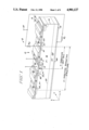
- FIG. 1 is a perspective cross-section view of a first embodiment of a circuit in accordance with the present invention
- FIGS. 2-4 illustrate perspective cross-section views of alternative embodiments of a circuit in accordance with the present invention
- FIGS. 5-8 illustrate measured operating characteristics of devices and circuits in accordance with the invention.
- a circuit 8 includes a semiconductor device 10 comprising a body of semiconductor material 12 having upper and lower major surfaces 13 and 14, respectively.
- the semiconductor device is a multicellular device and FIG. 1 shows several X-direction cells.
- the semiconductor body includes a lightly doped P type (P-) drift region 16 disposed between the upper and lower surfaces. Region 16 extends to the upper surface 13.
- a base region 18 extends into the drift region 16 from the upper surface 13 and forms a PN junction 17 with the drift region.
- the base region 18 is sometimes referred to as the body region of the FET, however, in this specification, the region 18 will be referred to as a base region to avoid confusion with the reference to the chip or wafer as a body of semiconductor material.
- a source/emitter region 20 is disposed in the base region 18, forms a PN junction 19 therewith and extends to the upper surface 13.
- a channel portion 18C of the base region is disposed adjacent the upper surface 13 between the source/emitter region 20 and the drift region 16.
- a drain region 22 is spaced from the base region 18 and extends into the drift region 16 from the upper surface 13 of the semiconductor body and forms an interface 21 therewith.
- the drain region is P type material, but more heavily doped than the drift region 16.
- the base, source/emitter and drain regions are each elongated in the Y-direction with the base and drain regions spaced apart in the X-direction.
- the individual cells are arranged as parallel, straight, Y-direction extending stripes.
- a collector region 24 of N type material extends from the second surface 14 toward the first surface 13, forms a PN junction 23 with the drift region and everywhere spaces the drift region 16 from the lower surface 14. Other collector region configurations may be employed, if desired.
- An insulated gate electrode 31 is disposed on the upper surface 13 over the channel portion 18C of the base region.
- the insulated gate electrode 31 is comprised of an insulating layer 30 and a conductor layer 32 and is provided to control the conductivity of the channel region 18C of the base region for holes, i.e. the majority carriers in the source/emitter and drift regions.
- the insulating layer 30 continues along the upper surface toward the drain region to serve as a field oxide and passivation layer protecting that portion of the semiconductor surface.
- the FIG. 1 structure combines a lateral MOSFET and a vertical IGBT in the same structure with shared common source/emitter, base and drift regions and a common insulated gate electrode.
- An first main electrode 34 is disposed on the upper surface 13 in ohmic contact with both the base region 18 and the source/emitter region 20.
- the electrode 34 serves as a first main terminal for the circuit.
- a drain electrode 36 is disposed on the upper surface 13 in ohmic contact with the drain region 22 and a collector electrode 38 is disposed on the lower surface 14 in ohmic contact with the collector region 24.
- a drain/collector circuit is connected between the drain electrode 36 and the collector electrode 38 and includes resistors R D and R C and a terminal 37 which serves as the second main terminal of the device. Either of the resistors R D or R C may have a zero resistance in accordance with the particular operating characteristics desired for the circuit and either or both of R D and R C may be integrated within the semiconductor body.
- the drain/collector circuit may be more accurately described as being connected between the collector junction and the drift region/drain region interface 21.
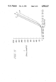
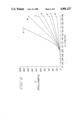
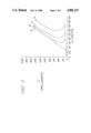
- FIGS. 5 and 6 The operating characteristics of experimental devices of this type are illustrated in FIGS. 5 and 6. These devices were fabricated with a vertical drift region thickness of 50 microns, a lateral drift region length of 35 microns and a drift region doping concentration of 2 ⁇ 10 14 cm --3 which are typical values for a 500 volt P channel device. The actual breakdown voltage of these devices could not be meaningfully determined because the test devices lacked edge terminations and therefore had actual breakdown voltages in the neighborhood of 20 volts.
- the operating characteristics are shown in FIG. 5 for the situation in which R C is equal to zero and in which R D was A ⁇ (drain open), B 100 ⁇ , C 50 ⁇ , and D 0106 .
- the current and voltage are measured across the terminals 34 and 37 and the gate electrode was held at -15 volts relative to electrode 34. As can be seen from these curves, as the drain resistance is reduced, the conductivity modulation within the drift region is reduced. This results in an increase in ON-resistance.
- FIG. 6 illustrates the operating characteristics of these devices for the situation in which the resistance R D is zero and the resistance R C is A 0 ⁇ , B 5 ⁇ , C 10 ⁇ , D 15 ⁇ , E 30 ⁇ , F 50 ⁇ , and G ⁇ (collector open). As can be seen from these curves, as the collector resistance is reduced, the ON-resistance decreases. This is a result of increasing modulation.
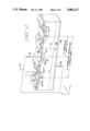
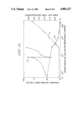
- FIG. 2 An alternative embodiment of a circuit in accordance with the present invention is illustrated in FIG. 2 where the IGBT is a lateral device and the MOSFET is a vertical device. Corresponding reference numerals are used in FIGS. 1 and 2 because of the similarity of device structure and operation.
- This structure includes a P type buffer portion 26 of the drift region 16 adjacent to the collector region 24. This buffer portion is introduced in order to prevent punch-through from the P- drift region to N+ collector region when the device is under high voltages without requiring excessive lateral spacing between the base and collector regions.
- a similar buffer region or layer may be included in the FIG. 1 device if a thinner drift region is desired. The operating characteristics of this device are shown in FIG.
- FIG. 3 A further alternative embodiment is illustrated in FIG. 3 in which all the electrodes are on the upper surface of the device, whereby both the MOSFET and the IGBT are lateral devices.
- the FIG. 3 structure is not preferred because of the relatively long path length during turn-off for extracting, through the drain region, carriers stored beneath the collector region.
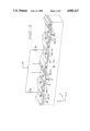
- FIG. 4 An alternative configuration for an all-lateral device version of this circuit is shown in FIG. 4.
- the major difference between the FIG. 3 and FIG. 4 structures is the close proximity of the collector and drain regions in FIG. 4. This close proximity has several effects.
- metallization patterning is more complex. The reduction in collector injection is minimized by positioning the drain region between two collector regions or in an aperture in a single collector region in which the two segments shown are connected at the Y-direction ends of the collector stripes or at other locations not shown in FIG. 4.
- the metallization patterning complexity can be reduced by providing a single common metallization for the collector and drain regions and providing fixed values for R D and R C by adjusting collector and drain doping concentrations.
- one of the collector region segments may be omitted, thereby narrowing the unit cell and providing a drain/collector structure which has different structures as seen from the two adjacent base regions.
- R D and R C values can be built into the device structure during the fabrication process.
- the resistor R D may be built into the drain region by reducing its doping concentration to increase the resistivity of the drain region and thereby incorporate the drain resistance into the drain region.
- the collector resistance can be built into the collector region by reducing its doping level to increase its resistivity. It is noted, that because of the effect of collector region doping concentration on collector injection efficiency, reducing the collector doping in order to increase its resistance also has an effect on the injection efficiency of the collector region and thus conductivity modulation of the drift region.
- the resistances may be built into the drain and collector electrodes either within the metallization itself or as contact resistance at the metal/semiconductor interface.
- the drain/collector circuit can be integrated within the semiconductor body if desired.
- this device For greatest versatility, it is preferred to fabricate this device with the internal R D and R C as small as device fabrication processes allow in order that the trade-off between ON-resistance and turn-off time may be controlled by externally provided resistors.
- resistors may be built into the device structure itself in order to reduce packaging costs, package size and external circuit complexity.
- the cells of this multicellular device have been shown and described as being parallel, elongated in the Y-direction (straight stripe) cells.
- the invention is equally applicable to rectangular, including square; hexagonal; and round, including circular; cell configurations, whether arranged in an array of uniform cells or as concentric cells of increasing circumference.
Landscapes
- Insulated Gate Type Field-Effect Transistor (AREA)
Abstract
Description
______________________________________
R.sub.D      R.sub.C
                   Turn-off Time (μs)
______________________________________
0            0     <0.22
∞      0     4.3
100Ω   0     1.65
30Ω    0     0.36
______________________________________
Claims (31)
Priority Applications (1)
| Application Number | Priority Date | Filing Date | Title |
|---|---|---|---|
| US07/254,897 US4901127A (en) | 1988-10-07 | 1988-10-07 | Circuit including a combined insulated gate bipolar transistor/MOSFET |
Applications Claiming Priority (1)
| Application Number | Priority Date | Filing Date | Title |
|---|---|---|---|
| US07/254,897 US4901127A (en) | 1988-10-07 | 1988-10-07 | Circuit including a combined insulated gate bipolar transistor/MOSFET |
Publications (1)
| Publication Number | Publication Date |
|---|---|
| US4901127A true US4901127A (en) | 1990-02-13 |
Family
ID=22966005
Family Applications (1)
| Application Number | Title | Priority Date | Filing Date |
|---|---|---|---|
| US07/254,897 Expired - Lifetime US4901127A (en) | 1988-10-07 | 1988-10-07 | Circuit including a combined insulated gate bipolar transistor/MOSFET |
Country Status (1)
| Country | Link |
|---|---|
| US (1) | US4901127A (en) |
Cited By (39)
| Publication number | Priority date | Publication date | Assignee | Title |
|---|---|---|---|---|
| WO1991003078A1 (en) * | 1989-08-17 | 1991-03-07 | Ixys Corporation | Insulated gate thyristor with gate turn on and turn off |
| US5060194A (en) * | 1989-03-31 | 1991-10-22 | Kabushiki Kaisha Toshiba | Semiconductor memory device having a bicmos memory cell |
| US5060032A (en) * | 1987-09-30 | 1991-10-22 | Nec Corporation | Insulated gate transistor operable at a low-drain-source voltage |
| WO1991016730A1 (en) * | 1990-04-26 | 1991-10-31 | Lucas Industries Public Limited Company | Insulated gate bipolar transistor |
| US5105243A (en) * | 1987-02-26 | 1992-04-14 | Kabushiki Kaisha Toshiba | Conductivity-modulation metal oxide field effect transistor with single gate structure |
| US5155574A (en) * | 1990-03-20 | 1992-10-13 | Mitsubishi Denki Kabushiki Kaisha | Semiconductor device |
| US5198688A (en) * | 1989-03-06 | 1993-03-30 | Fuji Electric Co., Ltd. | Semiconductor device provided with a conductivity modulation MISFET |
| US5237186A (en) * | 1987-02-26 | 1993-08-17 | Kabushiki Kaisha Toshiba | Conductivity-modulation metal oxide field effect transistor with single gate structure |
| US5381025A (en) * | 1989-08-17 | 1995-01-10 | Ixys Corporation | Insulated gate thyristor with gate turn on and turn off |
| US5396119A (en) * | 1992-04-17 | 1995-03-07 | Sgs-Thomson Microelectronics S.R.L. | MOS power transistor device with temperature compensation |
| EP0729186A1 (en) * | 1995-02-24 | 1996-08-28 | Consorzio per la Ricerca sulla Microelettronica nel Mezzogiorno - CoRiMMe | MOS-technology power device integrated structure and manufacturing process thereof |
| US5652540A (en) * | 1992-10-26 | 1997-07-29 | U S Philips Corporation | Current sensing circuit having at least one sense cell |
| EP0730308A3 (en) * | 1995-03-01 | 1997-09-03 | Siemens Ag | Integrated circuit device with at least one IGBT |
| US5665988A (en) * | 1995-02-09 | 1997-09-09 | Fuji Electric Co., Ltd. | Conductivity-modulation semiconductor |
| US5780917A (en) * | 1992-04-03 | 1998-07-14 | Hitachi, Ltd. | Composite controlled semiconductor device and power conversion device using the same |
| US5798554A (en) * | 1995-02-24 | 1998-08-25 | Consorzio Per La Ricerca Sulla Microelettronica Nel Mezzogiorno | MOS-technology power device integrated structure and manufacturing process thereof |
| US5841167A (en) * | 1995-12-28 | 1998-11-24 | Sgs-Thomson Microelectronics S.R.L. | MOS-technology power device integrated structure |
| US5877047A (en) * | 1997-08-15 | 1999-03-02 | Motorola, Inc. | Lateral gate, vertical drift region transistor |
| US5900662A (en) * | 1995-11-06 | 1999-05-04 | Sgs Thomson Microelectronics S.R.L. | MOS technology power device with low output resistance and low capacitance, and related manufacturing process |
| US5936454A (en) * | 1993-06-01 | 1999-08-10 | Motorola, Inc. | Lateral bipolar transistor operating with independent base and gate biasing |
| US5981998A (en) * | 1995-10-30 | 1999-11-09 | Sgs-Thomson Microelectronics S.R.L. | Single feature size MOS technology power device |
| US6030870A (en) * | 1995-10-30 | 2000-02-29 | Sgs-Thomson Microelectronics, S.R.L. | High density MOS technology power device |
| US6090669A (en) * | 1995-10-09 | 2000-07-18 | Consorzio Per La Ricerca Sulla Microelectronics Nel Mezzogiorno | Fabrication method for high voltage devices with at least one deep edge ring |
| US6104233A (en) * | 1990-04-13 | 2000-08-15 | Kabushiki Kaisha Toshiba | Substrate structure of semi-conductor device |
| US6228719B1 (en) | 1995-11-06 | 2001-05-08 | Stmicroelectronics S.R.L. | MOS technology power device with low output resistance and low capacitance, and related manufacturing process |
| US20020048915A1 (en) * | 1998-12-04 | 2002-04-25 | Daniel Reznik | Power semiconductor switch |
| US20020063280A1 (en) * | 1999-08-19 | 2002-05-30 | Gerald Deboy | Vertically structured power semiconductor component |
| US6399998B1 (en) * | 2000-09-29 | 2002-06-04 | Rockwell Technologies, Llc | High voltage insulated-gate bipolar switch |
| US6448616B1 (en) * | 2001-08-14 | 2002-09-10 | Telefonaktiebolaget Lm Ericsson | Adaptive biasing of RF power transistors |
| US6492691B2 (en) | 1998-05-26 | 2002-12-10 | Stmicroelectronics S.R.L. | High integration density MOS technology power device structure |
| US20030122222A1 (en) * | 2001-12-27 | 2003-07-03 | Hideki Okumura | Semiconductor device having vertical metal insulator semiconductor transistor and method of manufacturing the same |
| US6627961B1 (en) | 2000-05-05 | 2003-09-30 | International Rectifier Corporation | Hybrid IGBT and MOSFET for zero current at zero voltage |
| EP2117121A1 (en) | 2008-05-06 | 2009-11-11 | Schleifring und Apparatebau GmbH | Semiconductor power switch |
| WO2010057340A1 (en) * | 2008-11-19 | 2010-05-27 | 深圳市联德合微电子有限公司 | Integrated circuit utilizing ligbt output stage |
| GB2482479A (en) * | 2010-08-02 | 2012-02-08 | Univ Warwick | Semiconductor device operable as a vertical MOSFET and as a lateral insulated gate bipolar transistor, comprising a Schottky diode in the injector region. |
| CN102593166A (en) * | 2011-01-13 | 2012-07-18 | 茂达电子股份有限公司 | Insulated Gate Bipolar Transistor with High Operational Response Speed |
| CN102005473B (en) * | 2009-08-28 | 2012-10-17 | 比亚迪股份有限公司 | IGBT with improved termination |
| CN105408741A (en) * | 2013-06-20 | 2016-03-16 | 埃克隆德创新公司 | Integrated sensor device for charge detection |
| JP2016129192A (en) * | 2015-01-09 | 2016-07-14 | 株式会社デンソー | Semiconductor device |
Citations (2)
| Publication number | Priority date | Publication date | Assignee | Title |
|---|---|---|---|---|
| US4344081A (en) * | 1980-04-14 | 1982-08-10 | Supertex, Inc. | Combined DMOS and a vertical bipolar transistor device and fabrication method therefor |
| US4680604A (en) * | 1984-03-19 | 1987-07-14 | Kabushiki Kaisha Toshiba | Conductivity modulated MOS transistor device |
-
1988
- 1988-10-07 US US07/254,897 patent/US4901127A/en not_active Expired - Lifetime
Patent Citations (2)
| Publication number | Priority date | Publication date | Assignee | Title |
|---|---|---|---|---|
| US4344081A (en) * | 1980-04-14 | 1982-08-10 | Supertex, Inc. | Combined DMOS and a vertical bipolar transistor device and fabrication method therefor |
| US4680604A (en) * | 1984-03-19 | 1987-07-14 | Kabushiki Kaisha Toshiba | Conductivity modulated MOS transistor device |
Non-Patent Citations (6)
| Title |
|---|
| Chow, T., "A New Hybrid VDMOS-LIGBT Transistor", IEEE Electron Device Letters, vol. 9, No. 9, Sep. 1988, pp. 473-475. |
| Chow, T., A New Hybrid VDMOS LIGBT Transistor , IEEE Electron Device Letters, vol. 9, No. 9, Sep. 1988, pp. 473 475. * |
| Fossum, J. G. et al., "An Insightful Analysis of the Hybrid Insulated-Gate Bipolar Transistor", IEEE Transactions on Electron Devices, vol. 35, No. 9, Sep. 1988, pp. 1560-1562. |
| Fossum, J. G. et al., An Insightful Analysis of the Hybrid Insulated Gate Bipolar Transistor , IEEE Transactions on Electron Devices, vol. 35, No. 9, Sep. 1988, pp. 1560 1562. * |
| Liu, D. et al., "A Novel Trench-Injector Power Device with Low ON Resistance and High Switching Speed", IEEE Electron Device Letters, vol. 9, No. 7, Jul. 1988, pp. 321-323. |
| Liu, D. et al., A Novel Trench Injector Power Device with Low ON Resistance and High Switching Speed , IEEE Electron Device Letters, vol. 9, No. 7, Jul. 1988, pp. 321 323. * |
Cited By (59)
| Publication number | Priority date | Publication date | Assignee | Title |
|---|---|---|---|---|
| US5237186A (en) * | 1987-02-26 | 1993-08-17 | Kabushiki Kaisha Toshiba | Conductivity-modulation metal oxide field effect transistor with single gate structure |
| US5105243A (en) * | 1987-02-26 | 1992-04-14 | Kabushiki Kaisha Toshiba | Conductivity-modulation metal oxide field effect transistor with single gate structure |
| US5060032A (en) * | 1987-09-30 | 1991-10-22 | Nec Corporation | Insulated gate transistor operable at a low-drain-source voltage |
| US5198688A (en) * | 1989-03-06 | 1993-03-30 | Fuji Electric Co., Ltd. | Semiconductor device provided with a conductivity modulation MISFET |
| US5060194A (en) * | 1989-03-31 | 1991-10-22 | Kabushiki Kaisha Toshiba | Semiconductor memory device having a bicmos memory cell |
| US5381025A (en) * | 1989-08-17 | 1995-01-10 | Ixys Corporation | Insulated gate thyristor with gate turn on and turn off |
| WO1991003078A1 (en) * | 1989-08-17 | 1991-03-07 | Ixys Corporation | Insulated gate thyristor with gate turn on and turn off |
| US5155574A (en) * | 1990-03-20 | 1992-10-13 | Mitsubishi Denki Kabushiki Kaisha | Semiconductor device |
| US6104233A (en) * | 1990-04-13 | 2000-08-15 | Kabushiki Kaisha Toshiba | Substrate structure of semi-conductor device |
| WO1991016730A1 (en) * | 1990-04-26 | 1991-10-31 | Lucas Industries Public Limited Company | Insulated gate bipolar transistor |
| US5945723A (en) * | 1992-04-02 | 1999-08-31 | Hitachi, Ltd. | Composite controlled semiconductor device |
| US5780917A (en) * | 1992-04-03 | 1998-07-14 | Hitachi, Ltd. | Composite controlled semiconductor device and power conversion device using the same |
| US5396119A (en) * | 1992-04-17 | 1995-03-07 | Sgs-Thomson Microelectronics S.R.L. | MOS power transistor device with temperature compensation |
| US5652540A (en) * | 1992-10-26 | 1997-07-29 | U S Philips Corporation | Current sensing circuit having at least one sense cell |
| US5936454A (en) * | 1993-06-01 | 1999-08-10 | Motorola, Inc. | Lateral bipolar transistor operating with independent base and gate biasing |
| US5665988A (en) * | 1995-02-09 | 1997-09-09 | Fuji Electric Co., Ltd. | Conductivity-modulation semiconductor |
| US6111297A (en) * | 1995-02-24 | 2000-08-29 | Consorzio Per La Ricerca Sulla Microelettronica Nel Mezzogiorno | MOS-technology power device integrated structure and manufacturing process thereof |
| EP0729186A1 (en) * | 1995-02-24 | 1996-08-28 | Consorzio per la Ricerca sulla Microelettronica nel Mezzogiorno - CoRiMMe | MOS-technology power device integrated structure and manufacturing process thereof |
| US5798554A (en) * | 1995-02-24 | 1998-08-25 | Consorzio Per La Ricerca Sulla Microelettronica Nel Mezzogiorno | MOS-technology power device integrated structure and manufacturing process thereof |
| EP0730308A3 (en) * | 1995-03-01 | 1997-09-03 | Siemens Ag | Integrated circuit device with at least one IGBT |
| US5760424A (en) * | 1995-03-01 | 1998-06-02 | Siemens Aktiengesellschaft | Integrated circuit arrangement having at least one IGBT |
| US6090669A (en) * | 1995-10-09 | 2000-07-18 | Consorzio Per La Ricerca Sulla Microelectronics Nel Mezzogiorno | Fabrication method for high voltage devices with at least one deep edge ring |
| US6548864B2 (en) | 1995-10-30 | 2003-04-15 | Sgs Thomson Microelectronics | High density MOS technology power device |
| US5981343A (en) * | 1995-10-30 | 1999-11-09 | Sgs-Thomas Microelectronics, S.R.L. | Single feature size mos technology power device |
| US5985721A (en) * | 1995-10-30 | 1999-11-16 | Sgs-Thomson Microelectronics, S.R.L. | Single feature size MOS technology power device |
| US6030870A (en) * | 1995-10-30 | 2000-02-29 | Sgs-Thomson Microelectronics, S.R.L. | High density MOS technology power device |
| US6468866B2 (en) | 1995-10-30 | 2002-10-22 | Sgs-Thomson Microelectronics S.R.L. | Single feature size MOS technology power device |
| US5981998A (en) * | 1995-10-30 | 1999-11-09 | Sgs-Thomson Microelectronics S.R.L. | Single feature size MOS technology power device |
| US6566690B2 (en) | 1995-10-30 | 2003-05-20 | Sgs Thomson Microelectronics S.R.L. | Single feature size MOS technology power device |
| US5900662A (en) * | 1995-11-06 | 1999-05-04 | Sgs Thomson Microelectronics S.R.L. | MOS technology power device with low output resistance and low capacitance, and related manufacturing process |
| US6228719B1 (en) | 1995-11-06 | 2001-05-08 | Stmicroelectronics S.R.L. | MOS technology power device with low output resistance and low capacitance, and related manufacturing process |
| US6051862A (en) * | 1995-12-28 | 2000-04-18 | Sgs-Thomson Microelectronics S.R.L. | MOS-technology power device integrated structure |
| US5841167A (en) * | 1995-12-28 | 1998-11-24 | Sgs-Thomson Microelectronics S.R.L. | MOS-technology power device integrated structure |
| US5877047A (en) * | 1997-08-15 | 1999-03-02 | Motorola, Inc. | Lateral gate, vertical drift region transistor |
| US6492691B2 (en) | 1998-05-26 | 2002-12-10 | Stmicroelectronics S.R.L. | High integration density MOS technology power device structure |
| US20020048915A1 (en) * | 1998-12-04 | 2002-04-25 | Daniel Reznik | Power semiconductor switch |
| US6798040B2 (en) * | 1998-12-04 | 2004-09-28 | Infineon Technologies Ag | Power semiconductor switch |
| US20020063280A1 (en) * | 1999-08-19 | 2002-05-30 | Gerald Deboy | Vertically structured power semiconductor component |
| US6831327B2 (en) * | 1999-08-19 | 2004-12-14 | Infineon Technologies Ag | Vertically structured power semiconductor component |
| US6627961B1 (en) | 2000-05-05 | 2003-09-30 | International Rectifier Corporation | Hybrid IGBT and MOSFET for zero current at zero voltage |
| US6399998B1 (en) * | 2000-09-29 | 2002-06-04 | Rockwell Technologies, Llc | High voltage insulated-gate bipolar switch |
| US6448616B1 (en) * | 2001-08-14 | 2002-09-10 | Telefonaktiebolaget Lm Ericsson | Adaptive biasing of RF power transistors |
| US20030122222A1 (en) * | 2001-12-27 | 2003-07-03 | Hideki Okumura | Semiconductor device having vertical metal insulator semiconductor transistor and method of manufacturing the same |
| US6995426B2 (en) * | 2001-12-27 | 2006-02-07 | Kabushiki Kaisha Toshiba | Semiconductor device having vertical metal insulator semiconductor transistors having plural spatially overlapping regions of different conductivity type |
| US20060145290A1 (en) * | 2001-12-27 | 2006-07-06 | Hideki Okumura | Semiconductor device having vertical metal insulator semiconductor transistors having plural spatially overlapping regions of different conductivity type |
| EP2117121A1 (en) | 2008-05-06 | 2009-11-11 | Schleifring und Apparatebau GmbH | Semiconductor power switch |
| US20090296441A1 (en) * | 2008-05-06 | 2009-12-03 | Schleifring Und Apparatebau Gmbh | Semiconductor Power Switch |
| WO2010057340A1 (en) * | 2008-11-19 | 2010-05-27 | 深圳市联德合微电子有限公司 | Integrated circuit utilizing ligbt output stage |
| CN102005473B (en) * | 2009-08-28 | 2012-10-17 | 比亚迪股份有限公司 | IGBT with improved termination |
| GB2482479A (en) * | 2010-08-02 | 2012-02-08 | Univ Warwick | Semiconductor device operable as a vertical MOSFET and as a lateral insulated gate bipolar transistor, comprising a Schottky diode in the injector region. |
| GB2482479B (en) * | 2010-08-02 | 2015-02-18 | Univ Warwick | Semiconductor device |
| US20120181576A1 (en) * | 2011-01-13 | 2012-07-19 | Anpec Electronics Corporation | Insulated gate bipolar transistor |
| CN102593166A (en) * | 2011-01-13 | 2012-07-18 | 茂达电子股份有限公司 | Insulated Gate Bipolar Transistor with High Operational Response Speed |
| TWI424564B (en) * | 2011-01-13 | 2014-01-21 | Anpec Electronics Corp | Insulator gate with high operational response speed |
| CN105408741A (en) * | 2013-06-20 | 2016-03-16 | 埃克隆德创新公司 | Integrated sensor device for charge detection |
| EP3011327A4 (en) * | 2013-06-20 | 2017-03-01 | K. Eklund Innovation | An integrated sensor device for charge detection |
| US10209215B2 (en) | 2013-06-20 | 2019-02-19 | K.Eklund Innovation | Integrated circuit sensor device for charge detection hybridizing a lateral metal oxide semiconductor field effect transistor (MOSFET) and a vertical bipolar junction transistor (BJT) |
| CN105408741B (en) * | 2013-06-20 | 2019-04-02 | 埃克隆德创新公司 | Integrated sensor device for charge detection |
| JP2016129192A (en) * | 2015-01-09 | 2016-07-14 | 株式会社デンソー | Semiconductor device |
Similar Documents
| Publication | Publication Date | Title |
|---|---|---|
| US4901127A (en) | Circuit including a combined insulated gate bipolar transistor/MOSFET | |
| JP3911566B2 (en) | MOS type semiconductor device | |
| US5079608A (en) | Power MOSFET transistor circuit with active clamp | |
| US5631187A (en) | Method for making semiconductor device having high energy sustaining capability and a temperature compensated sustaining voltage | |
| US6169300B1 (en) | Insulated gate bipolar transistor with high dynamic ruggedness | |
| EP1187214B1 (en) | Semiconductor device with a protection against ESD | |
| US6246092B1 (en) | High breakdown voltage MOS semiconductor apparatus | |
| US6054728A (en) | Insulated gate thyristor | |
| US6580108B1 (en) | Insulated gate bipolar transistor decreasing the gate resistance | |
| EP0576001B1 (en) | Power semiconductor integrated circuit device with uniform electric field distribution | |
| EP2438618B1 (en) | Power switching devices having controllable surge current capabilities | |
| US9041120B2 (en) | Power MOS transistor with integrated gate-resistor | |
| US5341003A (en) | MOS semiconductor device having a main unit element and a sense unit element for monitoring the current in the main unit element | |
| US4721986A (en) | Bidirectional output semiconductor field effect transistor and method for its maufacture | |
| US4686551A (en) | MOS transistor | |
| US10811531B2 (en) | Transistor device with gate resistor | |
| EP3987661B1 (en) | Device design for short circuit protection of transistors | |
| US20040256659A1 (en) | MOS-gated transistor with improved UIS capability | |
| US11158627B2 (en) | Electronic circuit with a transistor device and a clamping circuit | |
| US6218888B1 (en) | Insulated gate bipolar transistor device with a current limiting circuit | |
| US10931276B1 (en) | Combined IGBT and superjunction MOSFET device with tuned switching speed | |
| EP1469523B1 (en) | A junction electronic component and an integrated power device incorporating said component | |
| EP0625797B1 (en) | Integrated structure current sensing resistor for power MOS devices, particularly for overload self-protected power MOS devices | |
| US5034790A (en) | MOS transistor with semi-insulating field plate and surface-adjoining top layer | |
| US4980741A (en) | MOS protection device |
Legal Events
| Date | Code | Title | Description |
|---|---|---|---|
| AS | Assignment |
Owner name: GENERAL ELECTRIC COMPANY, A NEW YORK CORP. Free format text: ASSIGNMENT OF ASSIGNORS INTEREST.;ASSIGNORS:CHOW, TAT-SING P.;BALIGA, BANTVAL J.;REEL/FRAME:004962/0211;SIGNING DATES FROM 19880930 TO 19881004 |
|
| FEPP | Fee payment procedure |
Free format text: PAYOR NUMBER ASSIGNED (ORIGINAL EVENT CODE: ASPN); ENTITY STATUS OF PATENT OWNER: LARGE ENTITY |
|
| STCF | Information on status: patent grant |
Free format text: PATENTED CASE |
|
| FEPP | Fee payment procedure |
Free format text: PAYER NUMBER DE-ASSIGNED (ORIGINAL EVENT CODE: RMPN); ENTITY STATUS OF PATENT OWNER: LARGE ENTITY Free format text: PAYOR NUMBER ASSIGNED (ORIGINAL EVENT CODE: ASPN); ENTITY STATUS OF PATENT OWNER: LARGE ENTITY |
|
| FPAY | Fee payment |
Year of fee payment: 4 |
|
| FPAY | Fee payment |
Year of fee payment: 8 |
|
| AS | Assignment |
Owner name: INTERSIL CORPORATION, FLORIDA Free format text: ASSIGNMENT OF ASSIGNORS INTEREST;ASSIGNOR:HARRIS CORPORATION;REEL/FRAME:010255/0405 Effective date: 19990813 |
|
| AS | Assignment |
Owner name: CREDIT SUISSE FIRST BOSTON, AS COLLATERAL AGENT, N Free format text: SECURITY INTEREST;ASSIGNOR:INTERSIL CORPORATION;REEL/FRAME:010351/0410 Effective date: 19990813 |
|
| AS | Assignment |
Owner name: INTERSIL HOLDING CORPORATION, CALIFORNIA Free format text: INTELLECTUAL PROPERTY PARTIAL RELEASE;ASSIGNOR:CREIDT SUISSE FIRST BOSTON;REEL/FRAME:011667/0166 Effective date: 20010303 |
|
| AS | Assignment |
Owner name: FAIRCHILD SEMICONDUCTOR CORPORATION, MAINE Free format text: REASSIGNMENT OF PATENT APPLICATIONS;ASSIGNOR:INTERSIL CORPORATION;REEL/FRAME:012002/0206 Effective date: 20010406 |
|
| FPAY | Fee payment |
Year of fee payment: 12 |