US4900955A - Voltage sharing circuit - Google Patents
Voltage sharing circuit Download PDFInfo
- Publication number
- US4900955A US4900955A US07/369,785 US36978589A US4900955A US 4900955 A US4900955 A US 4900955A US 36978589 A US36978589 A US 36978589A US 4900955 A US4900955 A US 4900955A
- Authority
- US
- United States
- Prior art keywords
- voltage
- active electronic
- electronic device
- electrode
- electrodes
- Prior art date
- Legal status (The legal status is an assumption and is not a legal conclusion. Google has not performed a legal analysis and makes no representation as to the accuracy of the status listed.)
- Expired - Fee Related
Links
Images
Classifications
-
- H—ELECTRICITY
- H03—ELECTRONIC CIRCUITRY
- H03K—PULSE TECHNIQUE
- H03K17/00—Electronic switching or gating, i.e. not by contact-making and –breaking
- H03K17/10—Modifications for increasing the maximum permissible switched voltage
- H03K17/102—Modifications for increasing the maximum permissible switched voltage in field-effect transistor switches
Definitions
- This invention relates to high voltage, high speed circuits and, more particularly, to such circuits in which the required voltage swings exceed the voltage rating of semiconductor devices which can operate at the required high speed.
- a voltage sharing circuit which allows the use of low voltage FETs to obtain high voltage outputs.
- a stack of FET devices is connected in series with the drain electrode of one FET connected to the source electrode of the next FET in the stack.
- An input signal is applied to the gate electrode of the first FET at one end of the stack and the output signal is derived at the drain electrode at the nth FET at the other end of the stack.
- Diodes are connected between reference voltages and the gate electrodes of each of the FETs except for the first or input FET.
- the reference voltages are selected in order to limit the maximum voltage which can be developed across all of the FETs except for the nth FET.
- the gate bias is provided by a resistor from drain to gate and is, then, limited
- the reference voltages can be tapered so that the lower the FET is in the stack the less the maximum voltage which is permitted to develop across the FET.
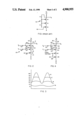
- FIG. 1 is a schematic of a voltage sharing circuit employing a resistive divider network
- FIG. 2 is a schematic of a voltage sharing circuit employing diode limiters in accordance with the principles of this invention
- FIG. 3 is a series of waveforms illustrating the signals taken at various points of the schematic of FIG. 2;
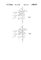
- FIG. 4 is a schematic of a voltage sharing circuit like that of FIG. 2 with the addition of a common cascode device.
- FIG. 5 is a schematic diagram of another voltage sharing circuit employing diode limiters in accordance with the principles of this invention.
- FIG. 6 is a schematic diagram of yet another voltage sharing circuit employing diode limiters in accordance with the principles of this invention.
- FIG. 2 of the drawings there is illustrated a voltage sharing amplifier 20 configured in accordance with the principles of this invention.
- the amplifier includes a grounded source FET 22 having a second FET 24 and a third FET 26 connected in series therewith.
- the signal to be amplified is applied to the gate electrode 28 of FET 22 and the output from the amplifier is taken at the drain 30 of FET 26.
- the supply voltage V S for the circuit is connected to drain 30 via a resistor 32.
- Reference voltages V 1 and V 2 are coupled to the gates 34 and 36 of FETs 24 and 26, respectively, through diodes 38 and 40.
- a resistor 42 is connected between gate 34 and the drain 44 of FET 24 and another resistor 46 is connected between gate 36 and drain 30 of FET 26.
- three FETs are shown, this is exemplary only. The number of devices required depends upon the required voltage swing and the rating of the devices. Thus, the circuit may employ only two devices or more than two devices.
- the individual FET devices of FIG. 2 are protected from excessive voltages while the output voltage (V 0 ) is beyond the rating of any one of the devices. Thus, large voltage swings are achieved with low voltage devices. The output voltage may exceed the ratings of any one of the devices by many times.
- V 1 is equal to the magnitude of V DSmax (the maximum drain to source voltage less the magnitude of V p (pinch off voltage) or
- V 2 is equal to V 1 +
- V 0 When the output voltage V 0 is nominally less than V 1 +
- the pinch off voltage is a worst case value.
- the reference voltage will be selected so that, for example, the second FET in the stack will start sharing voltage before it reaches V 1 +
- V p the second FET in the stack will start sharing voltage before it reaches V 1 +
- FIG. 3 illustrates the signals taken at various points in FIG. 2 and clearly shows the result of stacking FETs to obtain large voltage swings with low voltage devices.
- Waveforms A, B, C and D are taken at points A, B, C and D in FIG. 2.
- Stacked FET devices using a diode divider are very stable.
- the circuit has two states or modes of operation. When the voltage across the device is above the reference voltage, the diode will limit the gate voltage at the nominal reference voltage. Thus, in this mode the gate voltage is fixed and the circuit is a conventional cascode which is well known to be stable and desirable at high speeds. In the mode where the voltage drops below the reference voltage the diode is reverse biased and essentially does not exist. Therefore, the device is simply biased on by the resistor connecting the drain to the gate (resistors 42 and 46) and, thus, very stable in this state because the particular device is not acting as a linear element.
- the diodes are Schottky diodes because of their low capacitance and speed characteristics. While separate reference voltages are indicated, preferably the reference voltages are derived from a single source and divided with zener diodes which precisely define the reference voltage values.
- reference voltage V 1 would be less than
- V 2 may be made less than V 1 +
- FIG. 4 illustrates another embodiment of the invention. It is like the embodiment of FIG. 2 with the addition of another FET 50 as a cascode.
- This optional cascode is added to alleviate Miller effect on the input.
- the output voltage is nominally less than V 1 +
- the cure for this is to insert a cascode above it. Additional cascodes are not needed for the upper devices since they become cascodes inherently above some level and are short circuits otherwise.
- FIG. 5 of the drawings there is illustrates a voltage sharing amplifier 52 configured in accordance with the principles of this invention.
- FETs 22, 24 and 26 of FIG. 2 are replaced in FIG. 5 with bipolar devices 54, 56 and 58, each including a respective base electrode 60, 62 or 64.
- Bipolar device 58 includes collector electrode 66.
- Bipolar device 56 includes collector electrode 68.
- FIG. 6 of the drawings there is illustrates a voltage sharing amplifier 70 configured in accordance with the principles of this invention.
- FETs 22, 24 and 26 of FIG. 2 are replaced in FIG. 6 with vacuum tubes 72, 74 and 76, each including a respective grid electrode 78, 80 or 82.
- Vacuum tube 76 includes plate electrode 84.
- Vacuum tube 74 includes plate electrode 86.
- circuit describing the invention is an amplifier
- the principles of the invention are applicable to other types of circuitry where the output voltage exceeds the individual ratings of the semiconductors, such as switching circuits.
Landscapes
- Amplifiers (AREA)
- Tone Control, Compression And Expansion, Limiting Amplitude (AREA)
Abstract
Description
Claims (36)
Priority Applications (1)
| Application Number | Priority Date | Filing Date | Title |
|---|---|---|---|
| US07/369,785 US4900955A (en) | 1987-05-06 | 1989-06-19 | Voltage sharing circuit |
Applications Claiming Priority (2)
| Application Number | Priority Date | Filing Date | Title |
|---|---|---|---|
| US4779187A | 1987-05-06 | 1987-05-06 | |
| US07/369,785 US4900955A (en) | 1987-05-06 | 1989-06-19 | Voltage sharing circuit |
Related Parent Applications (1)
| Application Number | Title | Priority Date | Filing Date |
|---|---|---|---|
| US4779187A Continuation | 1987-05-06 | 1987-05-06 |
Publications (1)
| Publication Number | Publication Date |
|---|---|
| US4900955A true US4900955A (en) | 1990-02-13 |
Family
ID=26725433
Family Applications (1)
| Application Number | Title | Priority Date | Filing Date |
|---|---|---|---|
| US07/369,785 Expired - Fee Related US4900955A (en) | 1987-05-06 | 1989-06-19 | Voltage sharing circuit |
Country Status (1)
| Country | Link |
|---|---|
| US (1) | US4900955A (en) |
Cited By (16)
| Publication number | Priority date | Publication date | Assignee | Title |
|---|---|---|---|---|
| US5229662A (en) * | 1991-09-25 | 1993-07-20 | National Semiconductor Corporation | Logic circuit capable of operating with any one of a plurality of alternative voltage supply levels |
| EP0703665A3 (en) * | 1994-09-21 | 1997-09-24 | Nec Corp | Voltage level shift circuit |
| US5963076A (en) * | 1997-04-14 | 1999-10-05 | Motorola, Inc. | Circuit with hot-electron protection and method |
| US6072351A (en) * | 1997-08-18 | 2000-06-06 | Advanced Micro Devices, Inc. | Output buffer for making a 5.0 volt compatible input/output in a 2.5 volt semiconductor process |
| US6351157B1 (en) | 1997-08-18 | 2002-02-26 | Vantis Corporation | Output buffer for making a high voltage (5.0 volt) compatible input/output in a low voltage (2.5 volt) semiconductor process |
| US6525896B2 (en) | 1998-05-14 | 2003-02-25 | International Business Machines Corporation | Method and circuitry for high voltage application with MOSFET technology |
| US6617906B1 (en) * | 2002-10-01 | 2003-09-09 | Texas Instruments Incorporated | Low-current compliance stack using nondeterministically biased Zener strings |
| EP1624571A1 (en) * | 2004-08-06 | 2006-02-08 | ATMEL Germany GmbH | Circuit with active switch element and high withstand voltage |
| US7786807B1 (en) * | 2009-04-23 | 2010-08-31 | Broadcom Corporation | Cascode CMOS RF power amplifier with programmable feedback cascode bias under multiple supply voltages |
| WO2011022551A1 (en) * | 2009-08-19 | 2011-02-24 | Qualcomm Incorporated | Stacked amplifier with diode-based biasing |
| US20110050318A1 (en) * | 2009-08-26 | 2011-03-03 | Alfred E. Mann Foundation For Scientific Research | High voltage differential pair and op amp in low voltage process |
| US20110050331A1 (en) * | 2009-08-26 | 2011-03-03 | Alfred E. Mann Foundation For Scientific Research | High voltage current source and voltage expander in low voltage process |
| WO2013034509A1 (en) * | 2011-09-09 | 2013-03-14 | Icsense Nv | Dc-dc converter circuit |
| US20130154710A1 (en) * | 2011-12-15 | 2013-06-20 | Silergy Semiconductor Technology (Hangzhou) Ltd | Adaptive cascode circuit using mos transistors |
| US9041433B2 (en) * | 2013-06-21 | 2015-05-26 | Infineon Technologies Austria Ag | System and method for driving transistors |
| US9537410B2 (en) | 2014-09-10 | 2017-01-03 | General Electric Company | System and method for series connecting electronic power devices |
Citations (10)
| Publication number | Priority date | Publication date | Assignee | Title |
|---|---|---|---|---|
| US27972A (en) * | 1860-04-24 | Johan deckelmann axd f | ||
| US3622899A (en) * | 1969-05-08 | 1971-11-23 | Hewlett Packard Co | High-voltage power amplifier circuit |
| US3671749A (en) * | 1971-02-17 | 1972-06-20 | Gen Electric | Simultaneous light triggering of thyristor arrays |
| US4070589A (en) * | 1976-10-29 | 1978-01-24 | The Singer Company | High speed-high voltage switching with low power consumption |
| US4283674A (en) * | 1978-07-19 | 1981-08-11 | Hitachi, Ltd. | Constant voltage output circuit |
| US4367421A (en) * | 1980-04-21 | 1983-01-04 | Reliance Electric Company | Biasing methods and circuits for series connected transistor switches |
| US4479094A (en) * | 1982-05-26 | 1984-10-23 | Raytheon Company | Differential amplifier |
| US4481483A (en) * | 1982-01-21 | 1984-11-06 | Clarion Co., Ltd. | Low distortion amplifier circuit |
| US4484151A (en) * | 1980-03-10 | 1984-11-20 | U.S. Philips Corporation | Amplifier circuit |
| US4677391A (en) * | 1984-11-23 | 1987-06-30 | Microwave Technology, Inc. | Series biasing scheme for field effect transistors |
-
1989
- 1989-06-19 US US07/369,785 patent/US4900955A/en not_active Expired - Fee Related
Patent Citations (10)
| Publication number | Priority date | Publication date | Assignee | Title |
|---|---|---|---|---|
| US27972A (en) * | 1860-04-24 | Johan deckelmann axd f | ||
| US3622899A (en) * | 1969-05-08 | 1971-11-23 | Hewlett Packard Co | High-voltage power amplifier circuit |
| US3671749A (en) * | 1971-02-17 | 1972-06-20 | Gen Electric | Simultaneous light triggering of thyristor arrays |
| US4070589A (en) * | 1976-10-29 | 1978-01-24 | The Singer Company | High speed-high voltage switching with low power consumption |
| US4283674A (en) * | 1978-07-19 | 1981-08-11 | Hitachi, Ltd. | Constant voltage output circuit |
| US4484151A (en) * | 1980-03-10 | 1984-11-20 | U.S. Philips Corporation | Amplifier circuit |
| US4367421A (en) * | 1980-04-21 | 1983-01-04 | Reliance Electric Company | Biasing methods and circuits for series connected transistor switches |
| US4481483A (en) * | 1982-01-21 | 1984-11-06 | Clarion Co., Ltd. | Low distortion amplifier circuit |
| US4479094A (en) * | 1982-05-26 | 1984-10-23 | Raytheon Company | Differential amplifier |
| US4677391A (en) * | 1984-11-23 | 1987-06-30 | Microwave Technology, Inc. | Series biasing scheme for field effect transistors |
Non-Patent Citations (2)
| Title |
|---|
| Glover, "Using Low Voltage Transistors in High Voltage Circuits", Jul. 6, 1964, Electronic Design, pp. 23-29. |
| Glover, Using Low Voltage Transistors in High Voltage Circuits , Jul. 6, 1964, Electronic Design, pp. 23 29. * |
Cited By (25)
| Publication number | Priority date | Publication date | Assignee | Title |
|---|---|---|---|---|
| US5229662A (en) * | 1991-09-25 | 1993-07-20 | National Semiconductor Corporation | Logic circuit capable of operating with any one of a plurality of alternative voltage supply levels |
| EP0703665A3 (en) * | 1994-09-21 | 1997-09-24 | Nec Corp | Voltage level shift circuit |
| US5963076A (en) * | 1997-04-14 | 1999-10-05 | Motorola, Inc. | Circuit with hot-electron protection and method |
| US6072351A (en) * | 1997-08-18 | 2000-06-06 | Advanced Micro Devices, Inc. | Output buffer for making a 5.0 volt compatible input/output in a 2.5 volt semiconductor process |
| US6351157B1 (en) | 1997-08-18 | 2002-02-26 | Vantis Corporation | Output buffer for making a high voltage (5.0 volt) compatible input/output in a low voltage (2.5 volt) semiconductor process |
| US6525896B2 (en) | 1998-05-14 | 2003-02-25 | International Business Machines Corporation | Method and circuitry for high voltage application with MOSFET technology |
| US6617906B1 (en) * | 2002-10-01 | 2003-09-09 | Texas Instruments Incorporated | Low-current compliance stack using nondeterministically biased Zener strings |
| EP1624571A1 (en) * | 2004-08-06 | 2006-02-08 | ATMEL Germany GmbH | Circuit with active switch element and high withstand voltage |
| US20060028901A1 (en) * | 2004-08-06 | 2006-02-09 | Christoph Bromberger | Circuit layout with active components and high breakdown voltage |
| US7539965B2 (en) | 2004-08-06 | 2009-05-26 | Atmel Germany Gmbh | Circuit layout with active components and high breakdown voltage |
| US7786807B1 (en) * | 2009-04-23 | 2010-08-31 | Broadcom Corporation | Cascode CMOS RF power amplifier with programmable feedback cascode bias under multiple supply voltages |
| WO2011022551A1 (en) * | 2009-08-19 | 2011-02-24 | Qualcomm Incorporated | Stacked amplifier with diode-based biasing |
| US8847689B2 (en) | 2009-08-19 | 2014-09-30 | Qualcomm Incorporated | Stacked amplifier with diode-based biasing |
| US20110050318A1 (en) * | 2009-08-26 | 2011-03-03 | Alfred E. Mann Foundation For Scientific Research | High voltage differential pair and op amp in low voltage process |
| EP2293445A3 (en) * | 2009-08-26 | 2012-03-14 | Alfred E. Mann Foundation for Scientific Research | High voltage current source and voltage expander in low voltage process |
| US8339189B2 (en) | 2009-08-26 | 2012-12-25 | Alfred E. Mann Foundation For Scientific Research | High voltage current source and voltage expander in low voltage process |
| US20110050331A1 (en) * | 2009-08-26 | 2011-03-03 | Alfred E. Mann Foundation For Scientific Research | High voltage current source and voltage expander in low voltage process |
| WO2013034509A1 (en) * | 2011-09-09 | 2013-03-14 | Icsense Nv | Dc-dc converter circuit |
| BE1020663A5 (en) * | 2011-09-09 | 2014-02-04 | Icsence Nv | DC-DC CONVERTER CIRCUIT. |
| US20130154710A1 (en) * | 2011-12-15 | 2013-06-20 | Silergy Semiconductor Technology (Hangzhou) Ltd | Adaptive cascode circuit using mos transistors |
| US8570093B2 (en) * | 2011-12-15 | 2013-10-29 | Silergy Semiconductor Technology (Hangzhou) Ltd. | Adaptive cascode circuit using MOS transistors |
| US8717086B2 (en) | 2011-12-15 | 2014-05-06 | Silergy Semiconductor Technology (Hangzhou) Ltd | Adaptive cascode circuit using MOS transistors |
| US9041433B2 (en) * | 2013-06-21 | 2015-05-26 | Infineon Technologies Austria Ag | System and method for driving transistors |
| US9397636B2 (en) | 2013-06-21 | 2016-07-19 | Infineon Technologies Austria Ag | System and method for driving transistors |
| US9537410B2 (en) | 2014-09-10 | 2017-01-03 | General Electric Company | System and method for series connecting electronic power devices |
Similar Documents
| Publication | Publication Date | Title |
|---|---|---|
| US4900955A (en) | Voltage sharing circuit | |
| US4079336A (en) | Stacked transistor output amplifier | |
| US3531730A (en) | Signal translating stage providing direct voltage | |
| US6215356B1 (en) | Power amplifier arrangement | |
| US4780689A (en) | Amplifier input circuit | |
| US3900746A (en) | Voltage level conversion circuit | |
| US3217181A (en) | Logic switching circuit comprising a plurality of discrete inputs | |
| US2949543A (en) | Electronic amplifier | |
| US4808845A (en) | High voltage pulse generating semiconductor circuit with improved driving arrangement | |
| US5162749A (en) | Amplifier circuit having a feedback circuit | |
| JPH0763140B2 (en) | Gate circuit | |
| EP0189564B1 (en) | High to low transition speed up circuit for TTL-type gates | |
| JPS5983220A (en) | Reference voltage generation circuit | |
| US4400635A (en) | Wide temperature range switching circuit | |
| US4630046A (en) | Broadband switching network in matrix form | |
| US3487233A (en) | Detector with upper and lower threshold points | |
| EP0320582B1 (en) | Bicmos driver circuit including submicron on-chip voltage source | |
| US4587491A (en) | IC class AB amplifier output stage | |
| US3575614A (en) | Low voltage level mos interface circuit | |
| US3571616A (en) | Logic circuit | |
| US4808858A (en) | Dual limit programmable linear signal limiter | |
| US4128813A (en) | Amplifier | |
| US3553601A (en) | Transistor driver circuit | |
| US3422282A (en) | Level conversion circuit for interfacing logic systems | |
| US3219839A (en) | Sense amplifier, diode bridge and switch means providing clamped, noise-free, unipolar output |
Legal Events
| Date | Code | Title | Description |
|---|---|---|---|
| FPAY | Fee payment |
Year of fee payment: 4 |
|
| REMI | Maintenance fee reminder mailed | ||
| LAPS | Lapse for failure to pay maintenance fees | ||
| FP | Lapsed due to failure to pay maintenance fee |
Effective date: 19980218 |
|
| AS | Assignment |
Owner name: LOCKHEED SANDERS, INC., MARYLAND Free format text: CHANGE OF NAME;ASSIGNOR:SANDERS ASSOCIATES, INC.;REEL/FRAME:009570/0883 Effective date: 19900109 |
|
| AS | Assignment |
Owner name: LOCKHEED CORPORATION, MARYLAND Free format text: MERGER;ASSIGNOR:LOCKHEED SANDERS, INC.;REEL/FRAME:010859/0486 Effective date: 19960125 |
|
| AS | Assignment |
Owner name: LOCKHEED MARTIN CORPORATION, MARYLAND Free format text: MERGER;ASSIGNOR:LOCKHEED CORPORATION;REEL/FRAME:010871/0442 Effective date: 19960128 |
|
| FEPP | Fee payment procedure |
Free format text: PAYOR NUMBER ASSIGNED (ORIGINAL EVENT CODE: ASPN); ENTITY STATUS OF PATENT OWNER: LARGE ENTITY |
|
| STCH | Information on status: patent discontinuation |
Free format text: PATENT EXPIRED DUE TO NONPAYMENT OF MAINTENANCE FEES UNDER 37 CFR 1.362 |