US4876702A - Programmable time advance - Google Patents
Programmable time advance Download PDFInfo
- Publication number
- US4876702A US4876702A US07/225,123 US22512388A US4876702A US 4876702 A US4876702 A US 4876702A US 22512388 A US22512388 A US 22512388A US 4876702 A US4876702 A US 4876702A
- Authority
- US
- United States
- Prior art keywords
- signal
- clock
- clock signal
- advance
- circuit board
- Prior art date
- Legal status (The legal status is an assumption and is not a legal conclusion. Google has not performed a legal analysis and makes no representation as to the accuracy of the status listed.)
- Expired - Lifetime
Links
- 238000012360 testing method Methods 0.000 abstract description 145
- 239000004020 conductor Substances 0.000 abstract description 17
- 230000007274 generation of a signal involved in cell-cell signaling Effects 0.000 description 13
- 230000001360 synchronised effect Effects 0.000 description 7
- 238000011990 functional testing Methods 0.000 description 2
- 238000002347 injection Methods 0.000 description 2
- 239000007924 injection Substances 0.000 description 2
- 238000012544 monitoring process Methods 0.000 description 2
- 239000003990 capacitor Substances 0.000 description 1
- 230000003111 delayed effect Effects 0.000 description 1
- 238000001914 filtration Methods 0.000 description 1
- 230000010354 integration Effects 0.000 description 1
- 230000000737 periodic effect Effects 0.000 description 1
- 239000000243 solution Substances 0.000 description 1
Images

Classifications
-
- G—PHYSICS
- G01—MEASURING; TESTING
- G01R—MEASURING ELECTRIC VARIABLES; MEASURING MAGNETIC VARIABLES
- G01R31/00—Arrangements for testing electric properties; Arrangements for locating electric faults; Arrangements for electrical testing characterised by what is being tested not provided for elsewhere
- G01R31/28—Testing of electronic circuits, e.g. by signal tracer
- G01R31/317—Testing of digital circuits
- G01R31/3181—Functional testing
- G01R31/319—Tester hardware, i.e. output processing circuits
- G01R31/31903—Tester hardware, i.e. output processing circuits tester configuration
- G01R31/31908—Tester set-up, e.g. configuring the tester to the device under test [DUT], down loading test patterns
- G01R31/3191—Calibration
-
- G—PHYSICS
- G01—MEASURING; TESTING
- G01R—MEASURING ELECTRIC VARIABLES; MEASURING MAGNETIC VARIABLES
- G01R31/00—Arrangements for testing electric properties; Arrangements for locating electric faults; Arrangements for electrical testing characterised by what is being tested not provided for elsewhere
- G01R31/28—Testing of electronic circuits, e.g. by signal tracer
- G01R31/317—Testing of digital circuits
- G01R31/3181—Functional testing
- G01R31/319—Tester hardware, i.e. output processing circuits
- G01R31/31917—Stimuli generation or application of test patterns to the device under test [DUT]
- G01R31/31922—Timing generation or clock distribution
Definitions
- This invention relates to printed circuit board test systems and, in particular, to apparatus for synchronizing the clock pulses of the printed circuit board test system with the clock pulses of the printed circuit board under test.
- a printed circuit board test system is a completely integrated set of resources that is used for testing analog, hybrid and digital circuits.
- the printed circuit board test system typically performs shorts and opens tests; analog, hybrid and digital cluster and functional tests on the devices that are mounted on the printed circuit board.
- the test sequences executed by the printed circuit board test system are programmed into the printed circuit board test system by a test engineer to match the operational requirements of the printed circuit board under test.
- the printed circuit board test system includes a plurality of signal generation circuits and signal detector circuits.
- the test engineer programs the printed circuit board test system to generate a timed sequence of signals of known magnitude, shape and duration.
- Electrical interconnection to the printed circuit board under test is accomplished through a "bed of nails" interface that consists of a plurality of electrically conductive pins in a prearranged pattern on the printed circuit board test system.
- the bed of nails is connected to the signal generation and signal detector circuits.
- the printed circuit board under test is placed on the bed of nails to electrically interconnect various test points on the printed circuit board under test with the printed circuit board test system.
- the programmable signal generation circuits are used to apply a timed sequence of signals to various ones of the pins in the bed of nails to drive the printed circuit board under test.
- the signal detector circuits are connected to other pins on the bed of nails to monitor the response of the printed circuit board under test to these applied test signals.
- a problem with this arrangement is that it is difficult to synchronize the clock signals on both the printed circuit board under test and the printed circuit board test system.
- the printed circuit board under test has a clock signal generator circuit which operates independently of the clock signal generator circuit on the printed circuit board test system.
- the two clocks are synchronized by the printed circuit board test system monitoring the clock signal generated by the printed circuit board under test and using a phase locked loop to adjust the clock frequency and phase of the clock signal generation circuit on the printed circuit board test system to match the clock signal generated by the printed circuit board under test.
- the problem with this arrangement is that there exists a finite timing difference between the clock signal generated by the printed circuit board test system and the clock signal generated by the printed circuit board under test, due to the fact that the printed circuit board test system driver circuits have a certain delay time.
- the two clock signals are synchronized at the input of the phase locked loop of the printed circuit board test system, when the clock signal generated by the printed circuit board test system is applied to the printed circuit board under test, there is a certain delay in the signal occasioned by the response time of the driver circuits and associated conductors.
- This apparatus functions to offset the inherent delay occasioned by the conductors and the driver circuits of the printed circuit board test system to provide a clock signal at the output of the printed circuit board test system that exactly matches the clock signal of the printed circuit board under test at the printed circuit board under test. This is accomplished by inserting a clock advance signal into the phase locked loop to advance the timing of the clock signal generator circuit in the printed circuit board test system to compensate for the delay occasioned by the phase locked loop and driver circuits in the printed circuit board test system.
- the clock signal generation circuit in the printed circuit board test system consists of a voltage controlled oscillator which generates a clock signal at a predetermined center frequency, which clock signal is adjustable by a control signal applied to the voltage controlled oscillator.
- the clock signal generated by the voltage controlled oscillator is applied along with the clock signal from the printed circuit board under test to the input of a phase detector.
- the phase detector compares the two clock signals and generates a clock adjust signal that is indicative of both the direction and the magnitude of the difference between these two clock signals.
- This clock adjust signal is applied to the voltage controlled oscillator to adjust the center frequency of the clock signal generated therein to synchronize the clock signal generated by the voltage controlled oscillator to the clock signal obtained from the printed circuit board under test.
- the programmable time advance circuit compensates for the delay in the clock signal generated by the voltage controlled oscillator and applied by the driver circuit to the printed circuit board under test by injecting a clock advance signal into the phase detector portion of the phase locked loop.
- This clock advance signal is a signal of fixed magnitude and duration that matches the measured time delay occasioned by the response time of the conductors and the response time of the driver circuits of the printed circuit board test system.
- the clock advance signal time shifts the clock signal generated by the voltage controlled oscillator to offset the delay time occasioned by the conductors and driver circuits while the clock adjust signal from the phase detector 21 adjusts the frequency of the clock signal generated by the voltage-controlled oscillator to match the clock signal generated by the printed circuit board under test.
- the clock advance signal is programmable so that a user-definable fixed amount of time advance can be provided in this system.
- FIG. 1 illustrates a phase locked loop (PLL) with time advance circuit
- FIG. 2 illustrates the programmable time advance circuit
- FIG. 3 illustrates timing signal wave forms for the programmable time advance circuit.
- a printed circuit board test system is a completely integrated set of resources that is used for testing analog, hybrid and digital circuits.
- the printed circuit board test system typically performs shorts and opens tests; analog, hybrid and digital in-circuit tests; and analog, hybrid and digital cluster and functional tests on the devices that are mounted on the printed circuit board.
- the test sequences executed by the printed circuit board test system are programmed into the printed circuit board test system by a test engineer to match the operational requirements of the printed circuit board under test.
- the printed circuit board test system includes a plurality of signal generation circuits and signal detector circuits.
- the test engineer programs the printed circuit board test system to generate a timed sequence of signals of known magnitude, shape and duration.
- Electrical interconnection to the printed circuit board under test is accomplished through a "bed of nails" interface that consists of a plurality of electrically conductive pins in a prearranged pattern on the printed circuit board test system.
- the bed of nails is connected to the signal generation and signal detector circuits.
- the printed circuit board under test is placed on the bed of nails to electrically interconnect various test points on the printed circuit board under test with the printed circuit board test system.
- the programmable signal generation circuits are used to apply a timed sequence of signals to various ones of the pins in the bed of nails to drive the printed circuit board under test.
- the signal detector circuits are connected to other pins on the bed of nails to monitor the response of the printed circuit board under test to these applied test signals.
- a problem with this arrangement is that it is difficult to synchronize the clock signals on both the printed circuit board under test and the printed circuit board test system.
- the printed circuit board under test has a clock signal generator circuit which operates independently of the clock signal generator circuit on the printed circuit board test system.
- the two clocks are synchronized by the printed circuit board test system monitoring the clock signal generated by the printed circuit board under test and using a phase locked loop to adjust the clock frequency and phase of the clock signal generation circuit on the printed circuit board test system to match the clock signal generated by the printed circuit board under test.
- the problem with this arrangement is that there exists a finite timing difference between the clock signal generated by the printed circuit board test system and the clock signal generated by the printed circuit board under test, due to the fact that the printed circuit board test system conductors and driver circuits have a certain delay time.
- the two clock signals are synchronized at the input of the phase locked loop of the printed circuit board test system, when the clock signal generated by the printed circuit board test system is applied to the printed circuit board under test there is a certain delay in the signal occasioned by the response time of the driver circuits and associated conductors.
- the programmable time advance circuit of the present invention functions to offset the inherent delay occasioned by the conductors and the driver circuits to provide a clock signal at the output of the printed circuit board test system that exactly matches the clock signal of the printed circuit board under test at the printed circuit board under test. This is accomplished by inserting a clock advance signal into the phase locked loop to advance the timing of the clock signal generator circuit in the printed circuit board test system to compensate for the delay occasioned by the conductors and driver circuits in the printed circuit board test system.
- the clock signal generation circuit in the printed circuit board test system consists of a voltage controlled oscillator which generates a clock signal at a predetermined center frequency, which clock signal is adjustable by a control signal applied to the voltage controlled oscillator.
- the clock signal generated by the voltage controlled oscillator is applied along with the clock signal from the printed circuit board under test to the input of a phase detector.
- the phase detector compares the two clock signals and generates a clock adjust signal that is indicative of both the direction and the magnitude of the difference between these two clock signals.
- This clock adjust signal is applied to the voltage controlled oscillator to adjust the center frequency of the clock signal generated therein to synchronize the clock signal generated by the voltage controlled oscillator to the clock signal obtained from the printed circuit board under test.
- the programmable time advance circuit compensates for the delay in the clock signal generated by the voltage controlled oscillator and applied by the driver circuit to the printed circuit board under test by injecting a clock advance signal into the phase detector portion of the phase locked loop.
- This clock advance signal is a signal of fixed magnitude and duration that matches the measured time delay occasioned by the response time of the conductors and the response time of the driver circuits of the printed circuit board test system.
- the clock advance signal time shifts the clock signal generated by the voltage controlled oscillator to offset the delay time occasioned by the conductors and driver circuits while the clock adjust signal from the phase detector adjusts the frequency of the clock signal generated by the voltage controlled oscillator to match the clock signal generated by the printed circuit board under test.
- the clock advance signal is programmable so that a user-definable fixed amount of time advance can be provided in this system.
- PPL Phase Locked Loop
- FIG. 1 shows a phase locked loop (PLL) made up of phase detector 140, loop filter 109 and voltage controlled oscillator (VCO) 101.
- PLL phase locked loop
- VCO voltage controlled oscillator
- programmable time advance circuit 104 is added to the PPL.
- phase detector 140 has two inputs R (reference) and V (VCO), and one output.
- the phase detector measures the difference, in time, between R and V and emits an output signal which is indicative of that difference.
- R is the reference signal on line 129
- V is the signal output by VCO 101 on line 105
- the output of phase detector 140 is emitted on line 123.
- the output signal on line 123 is an electrical charge.
- the operation of phase detector 140 can be represented mathematically as follows:
- phase detector 140 is the input to the loop filter 109 on line 123.
- loop filter 109 performs two functions:
- VCO 101 is a voltage controlled oscillator whose frequency output dependant on its voltage input.
- the operation of VCO 101 can be represented mathematically as follows:
- F o is the frequency output of VCO 101
- k vco is the VCO 101 tuning constant
- V in the VCO input voltage that is, the output of loop filter 109 on line 128 in FIG. 1).
- phase detector 140 measures the difference between the R input and V input and adjusts the frequency of VCO 101 (via loop filter 109) to equal the input frequency present at R.
- the loop is said to be "phase locked".
- the charge flowing into the loop filter must be zero, and the voltage output of the loop filter will be unchanging.
- Q adv represents the charge injected by advance circuit 104.
- Q adv is non-zero
- (t R -t V ) will also be non-zero and hence we have an offset in time between the R input and the V input.
- This offset can be either positive (R input lead V input) or negative (V input leads R input) by making Q adv positive or negative.
- FIG. 2 illustrates the programmable time advance circuit of the present invention.
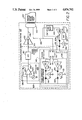
- a printed circuit board test system 107 which is interconnected through a "bed of nails" 100 to a printed circuit board under test 103.
- the printed circuit board under test 103 is assumed to have a clock signal generation circuit included therein.
- the output of the clock signal generation circuit of the printed circuit board under test 103 is conveyed by lead 129 in printed circuit board test system 107.
- Printed circuit board test system 107 includes a voltage controlled oscillator 101 which is interconnected via lead 105 to driver circuit 102.
- the clock signal generated by voltage controlled oscillator 101 is output via lead 105 to driver 102 where it is replicated and applied over lead 106 and bed of nails 100 to one or more predetermined leads on the printed circuit board under test 103.
- a phase locked loop 145 is provided to synchronize the output of the voltage controlled oscillator 101 with the clock signal generated by the printed circuit board under test 103.
- the phase locked loop 145 consists of phase detector 140, loop filter 109 and VCO 101.
- Phase detector 140 generates a clock adjust signal which is applied to voltage controlled oscillator 101 via loop filter 109.
- a programmable time advance circuit 104 is connected to the clock signal generated by the printed circuit board under test 103 to advance the clock signal generated by voltage controlled oscillator 101.
- the output signal of programmable time advance circuit 104 is connected to lead 123 which inputs this signal to voltage controlled oscillator 101 via loop filter 109.
- phase detector 140 includes a phase detector integrated circuit (IC) 110 that functions to measure the difference between the two clock signals applied to the input therein.
- Phase detector IC 110 is a device well known in the art and, for example, would be a Motorola MC 12040 device.
- Phase detector IC 110 determines the magnitude and direction of the difference between the reference clock signal which is obtained from printed circuit board under test 103 on lead 129 and the clock signal generated by voltage controlled oscillator 101 as applied to lead 105.
- Phase detector IC 110 has two output terminals labeled U and D, which output terminals are used to indicate that the generated clock signal is less than or greater than the reference clock signal in frequency, respectively.
- the signal generated by phase detector IC 110 at terminal U is applied via lead 111 to one input of phase correction current source circuit 108. This signal is applied to an inverting driver circuit 112 that drives lead 118.
- the signal appearing on lead 118 is an inverted replica of the signal output by phase detector IC 110 on lead 111.
- the magnitude, timing and duration of the signal on lead 111 is indicative of the time difference between the reference clock signal generated by printed circuit board under test 103 and the clock signal generated by voltage controlled oscillator 101.
- Phase detector IC 110 applies this signal to lead 111 when the clock signal generated by voltage controlled oscillator 101 is less than the clock signal generated by printed circuit board under test 103 in frequency. Otherwise, no signal is applied to lead 111 by phase detector circuit 110.
- the signal appearing on lead 111, as reproduced in inverted form on lead 118 controls the current switch made up of current source 117 and diodes 115 and 116. If the voltage at lead 118 is greater than the voltage on lead 123, diode 115 turns on, diode 116 turns off and all of current Ipc is drawn through diode 115.
- diode 115 turns off, diode 116 turns on and all of current Ipc is drawn through diode 116.
- the current drawn through diode 116 adjusts the clock signal as produced by voltage controlled oscillator 101 as is described below.
- phase detector IC 110 provides a signal indicative of the timing difference between the reference clock signal generated by printed circuit board under test 103 and the clock signal generated by voltage controlled oscillator 101 when the clock signal generated by voltage controlled oscillator 101 is greater in frequency then the clock signal generated by printed circuit board under test 103. Otherwise, no signal is applied to lead 113 by by phase detector IC 110.
- This correction signal applied to terminal D of phase detector IC 110 is carried by lead 113 to driver circuit 114, which replicates the signal onto lead 122.
- the signal appearing on lead 122 controls the current switch made up of current source 121 and diodes 119 and 120.
- diode 120 If the voltage at lead 122 is greater than the voltage on lead 123, diode 120 turns on, diode 119 turns off and all of current Ipc is drawn through diode 120. If the voltage at lead 122 is less than the voltage on lead 123, diode 120 turns off, diode 119 turns on and all of current Ipc is drawn through diode 119.
- phase correction current sources 108 thereby acts as a current switch that has three states: current source, current sink, no current.
- the correction signal applied through diode 116 or 120 by phase correction current source 108 is output on lead 123 to a loop filter 109 which functions as an integrator circuit to generate a control signal to modify the frequency of voltage controlled oscillator 101.
- phase detector IC 110 drives phase correction current sources 108 to produce a correction signal that is indicative of the phase offset of the input signals to phase detector circuit 110.
- This correction signal is applied to the inverting input of differential amplifier 124 whose non-inverting input is connected to the voltage reference source 125.
- Resistor 126 and capacitor 127 are connected between the inverting input of differential amplifier 124 and the output terminal of differential amplifier 124 to provide the integrating function.
- the output signal produced by loop filter 109 is applied via lead 128 to the input terminal of voltage controlled oscillator 101 to adjust the voltage controlled oscillator 101 so that the input signals to phase detector IC 110 do not exhibit any offset.
- programmable time advance circuit 104 provides a predetermined fixed advance to the clock signal generated by voltage controlled oscillator 101 to exactly offset the delay occasioned by leads 105, 106 and driver 102. This circuit therefore produces a clock signal applied to printed circuit board under test 103 that is exactly in synchronization with the clock signal generated by printed circuit board under test 103.
- This time advance is effectuated by programmable time advance circuit 104 injecting a fixed packet of charge per clock cycle into the summing node of the phase correction current sources 108.
- Feedback operation of the phase locked loop 145 that is implemented by phase detector 140, loop filter 109, and VCO 101 then adjusts the clock signal produced by VCO 101 until the inputs of the phase detector IC 110 are offset by precisely an amount to exactly cancel the delay occasioned by leads 105, 106 and driver 102.
- programmable time advance circuit 104 The operation of programmable time advance circuit 104 is initiated by the occurrence of a clock signal on lead 129, which clock signal is generated by printed circuit board under test 103.
- This clock signal triggers one shot circuit 131 to produce a pulse of fixed time duration delta-tqi.
- This pulse of fixed time duration is inverted by driver circuit 133 and switched through diode 134 to constant current source 136.
- This signal pulse applied by driver circuit 133 reverse biases switching diode 134 and thereby enables the current produced by constant current source 136 to be applied via switching diode 135 to the summing node of phase correction current sources 108.
- the magnitude of the current drawn by constant current source 136 is programmable in that a signal applied on data bus 138 to digital-to-analog converter circuit 137 defines the magnitude of the current produced by constant current source 136.
- the value of the current produced by constant current source 136 can be controlled with greater precision than the duration of the drive signal produced by one shot circuit 131.
- the printed circuit board test system 107 is programmed to establish a fixed value for the current Iq i drawn by constant current source 136. This current is applied for a predetermined period of time due to the action of one shot circuit 131 which triggers in synchronization with the clock signal produced by printed circuit board under test 103 to produce a pulse of fixed duration.
- Phase correction current sources 108 when switched on by phase detector circuit 110, apply a fixed value current to loop filter 109 for a length of time determined by the duration of the output signal produced by phase detector circuit 110.
- the charge removed from loop filter circuit 109 is equal to the current drawn by constant current source 136 multiplied by the length of time per clock cycle that constant current source 136 is enabled by one shot circuit 131 and its associated signal inverting driver circuit 133.
- the operation of programmable time advance circuit 104 when the PLL is locked, is mathematically described as follows:
- Ipc is fixed at 6 mA
- delta -- tqi is fixed at 20 nS
- Iqi can be a programmable current source (DAC).
- DAC programmable current source
- FIG. 3 illustrates various signal waveforms representative of the operation of the programmable time advance circuit 104.
- Square wave signals are illustrated for simplicity although periodic pulse signals or any other similar clock signal can be used.
- the first signal waveform shown on FIG. 3 is labeled R and is the reference clock signal obtained from printed circuit board under test 103 as applied to lead 129.
- the signal waveform labeled V is the clock signal generated by voltage controlled oscillator 101 and applied to lead 105, without the operation of programmable time advance circuit 104.
- the signal waveform V' is the clock signal V as it appears at printed circuit board under test 103.
- the clock signal is delayed by a time of t4-t3 due to the response time of driver 102 and the conductors 105, 106 and the conductors in bed of nails 100.
- Programmable time advance circuit 104 generates a clock advance signal such that the clock signal generated by voltage controlled oscillator 101 V" leads the reference clock signal generated by printed circuit board under test 103 by a time t3-t2 which time is exactly equal to the delay time t4-t3 occasioned by the response time of driver 102, conductors 105, 106 and bed of nails 100. Therefore, the clock signal applied to printed circuit board under test 103 by printed circuit board test system 107 is V"', which signal is exactly synchronized with the reference clock signal R generated by the clock signal generation circuit of printed circuit board under test 103.
Landscapes
- Engineering & Computer Science (AREA)
- General Engineering & Computer Science (AREA)
- Physics & Mathematics (AREA)
- General Physics & Mathematics (AREA)
- Tests Of Electronic Circuits (AREA)
- Stabilization Of Oscillater, Synchronisation, Frequency Synthesizers (AREA)
Abstract
Description
Q.sub.o =k.sub.pd *(t.sub.R -t.sub.V)
F.sub.o =k.sub.vco *V.sub.in
Q.sub.adv =-Q.sub.o =-k.sub.pd *(t.sub.R -t.sub.V)
______________________________________
          (charge dumped into summing node) =
          (charge pulled out of summing node)
          ** or **
          Ipc(delta --trv) = Iqi(delta --tqi)
where:    Ipc ->phase correction current
          sources (mA)
          delta --trv ->offset of inputs to the
          phase detector circuit 140
          Iqi ->charge injection current
          source (mA)
          delta --tqi ->fixed duration of the charge
          injection (nS)
______________________________________
______________________________________
delta --trv/Iqi = (delta tqi)/Ipc
=                 20 nS/6 mA
=                 3.33 nS/mA
______________________________________
Claims (16)
Priority Applications (4)
| Application Number | Priority Date | Filing Date | Title |
|---|---|---|---|
| US07/225,123 US4876702A (en) | 1988-07-28 | 1988-07-28 | Programmable time advance |
| EP89307556A EP0353027B1 (en) | 1988-07-28 | 1989-07-25 | Programmable time advance |
| DE68911410T DE68911410T2 (en) | 1988-07-28 | 1989-07-25 | Programmable time shift. |
| JP1196463A JP3054155B2 (en) | 1988-07-28 | 1989-07-28 | Time advance device |
Applications Claiming Priority (1)
| Application Number | Priority Date | Filing Date | Title |
|---|---|---|---|
| US07/225,123 US4876702A (en) | 1988-07-28 | 1988-07-28 | Programmable time advance |
Publications (1)
| Publication Number | Publication Date |
|---|---|
| US4876702A true US4876702A (en) | 1989-10-24 |
Family
ID=22843630
Family Applications (1)
| Application Number | Title | Priority Date | Filing Date |
|---|---|---|---|
| US07/225,123 Expired - Lifetime US4876702A (en) | 1988-07-28 | 1988-07-28 | Programmable time advance |
Country Status (4)
| Country | Link |
|---|---|
| US (1) | US4876702A (en) |
| EP (1) | EP0353027B1 (en) |
| JP (1) | JP3054155B2 (en) |
| DE (1) | DE68911410T2 (en) |
Cited By (3)
| Publication number | Priority date | Publication date | Assignee | Title |
|---|---|---|---|---|
| US5208838A (en) * | 1990-03-30 | 1993-05-04 | National Semiconductor Corporation | Clock signal multiplier |
| US5524114A (en) * | 1993-10-22 | 1996-06-04 | Lsi Logic Corporation | Method and apparatus for testing semiconductor devices at speed |
| US20010031507A1 (en) * | 2000-02-03 | 2001-10-18 | Simon Muff | Method and device for adapting/tuning signal transit times on line systems or networks between integrated circuits |
Families Citing this family (2)
| Publication number | Priority date | Publication date | Assignee | Title |
|---|---|---|---|---|
| DE60105297T2 (en) * | 2000-05-31 | 2005-11-17 | Broadcom Corp., Irvine | MULTIPROCESSOR COMPUTER BUS INTERFACE ADAPTER AND METHOD |
| CN102887595A (en) * | 2012-09-21 | 2013-01-23 | 江苏北辰环境科技有限公司 | Drift-type aerating device |
Citations (4)
| Publication number | Priority date | Publication date | Assignee | Title |
|---|---|---|---|---|
| US4105948A (en) * | 1977-04-18 | 1978-08-08 | Rca Corporation | Frequency synthesizer with rapidly changeable frequency |
| US4387351A (en) * | 1980-12-18 | 1983-06-07 | Motorola Inc. | Wideband FM modulator and AFC control loop therefor |
| US4419633A (en) * | 1980-12-29 | 1983-12-06 | Rockwell International Corporation | Phase lock loop |
| US4724401A (en) * | 1987-04-23 | 1988-02-09 | Rockwell International Corporation | Adaptive oscillator apparatus for use in a phase-lock loop |
Family Cites Families (2)
| Publication number | Priority date | Publication date | Assignee | Title |
|---|---|---|---|---|
| FR2480048A1 (en) | 1980-04-04 | 1981-10-09 | Labo Cent Telecommunicat | FREQUENCY LOCKING ANALOG LOOP |
| JPS63500676A (en) * | 1985-08-23 | 1988-03-10 | アウトルック・テクノロジ−・インク | Harmonic sampling logic analyzer |
-
1988
- 1988-07-28 US US07/225,123 patent/US4876702A/en not_active Expired - Lifetime
-
1989
- 1989-07-25 EP EP89307556A patent/EP0353027B1/en not_active Expired - Lifetime
- 1989-07-25 DE DE68911410T patent/DE68911410T2/en not_active Expired - Fee Related
- 1989-07-28 JP JP1196463A patent/JP3054155B2/en not_active Expired - Fee Related
Patent Citations (4)
| Publication number | Priority date | Publication date | Assignee | Title |
|---|---|---|---|---|
| US4105948A (en) * | 1977-04-18 | 1978-08-08 | Rca Corporation | Frequency synthesizer with rapidly changeable frequency |
| US4387351A (en) * | 1980-12-18 | 1983-06-07 | Motorola Inc. | Wideband FM modulator and AFC control loop therefor |
| US4419633A (en) * | 1980-12-29 | 1983-12-06 | Rockwell International Corporation | Phase lock loop |
| US4724401A (en) * | 1987-04-23 | 1988-02-09 | Rockwell International Corporation | Adaptive oscillator apparatus for use in a phase-lock loop |
Cited By (4)
| Publication number | Priority date | Publication date | Assignee | Title |
|---|---|---|---|---|
| US5208838A (en) * | 1990-03-30 | 1993-05-04 | National Semiconductor Corporation | Clock signal multiplier |
| US5524114A (en) * | 1993-10-22 | 1996-06-04 | Lsi Logic Corporation | Method and apparatus for testing semiconductor devices at speed |
| US20010031507A1 (en) * | 2000-02-03 | 2001-10-18 | Simon Muff | Method and device for adapting/tuning signal transit times on line systems or networks between integrated circuits |
| US6968481B2 (en) * | 2000-02-03 | 2005-11-22 | Infineon Technologies Ag | Method and device for adapting/tuning signal transit times on line systems or networks between integrated circuits |
Also Published As
| Publication number | Publication date |
|---|---|
| EP0353027A2 (en) | 1990-01-31 |
| JP3054155B2 (en) | 2000-06-19 |
| DE68911410D1 (en) | 1994-01-27 |
| JPH0275980A (en) | 1990-03-15 |
| DE68911410T2 (en) | 1994-05-26 |
| EP0353027A3 (en) | 1991-01-30 |
| EP0353027B1 (en) | 1993-12-15 |
Similar Documents
| Publication | Publication Date | Title |
|---|---|---|
| KR100201709B1 (en) | Timing signal generating circuit | |
| US5095262A (en) | Electro-optic sampling system clock and stimulus pattern generator | |
| US6275057B1 (en) | Semiconductor test system having high frequency and low jitter clock generator | |
| CN101150316B (en) | A multi-channel clock synchronization method and system | |
| EP0297719B1 (en) | Device for synchronizing the output pulses of a circuit with an input clock | |
| US7809052B2 (en) | Test circuit, system, and method for testing one or more circuit components arranged upon a common printed circuit board | |
| US4038612A (en) | Swept oscillator automatic linearizer | |
| PL195271B1 (en) | Method for tuning the bandwidth of a phase-locked loop | |
| JP3505011B2 (en) | High precision signal generation circuit | |
| US4849714A (en) | Signal generating apparatus | |
| US6378098B1 (en) | Semiconductor test system | |
| US5057771A (en) | Phase-locked timebase for electro-optic sampling | |
| US4876702A (en) | Programmable time advance | |
| JP3923150B2 (en) | Frequency synthesizer | |
| US5886536A (en) | Semiconductor tester synchronized with external clock | |
| JP2574194B2 (en) | Digital pulse generator | |
| US5488369A (en) | High speed sampling apparatus and method for calibrating the same | |
| JP2628182B2 (en) | Test equipment for analog-digital hybrid IC | |
| JP2842446B2 (en) | Test equipment for hybrid analog-digital ICs. | |
| JP2831744B2 (en) | Test equipment for analog-digital hybrid IC | |
| JP3008938B1 (en) | PLL circuit | |
| JP2008118338A (en) | Device for generating jitters | |
| JPH07209379A (en) | Semiconductor test device synchronized with outside clock | |
| KR0135736Y1 (en) | Clock generation circuit of digital CD camera | |
| EP0292515B1 (en) | A high speed sampling apparatus and method for calibrating the same |
Legal Events
| Date | Code | Title | Description |
|---|---|---|---|
| AS | Assignment |
Owner name: HEWLETT-PACKARD COMPANY, PALO ALTO, CA., A CORP OF Free format text: ASSIGNMENT OF ASSIGNORS INTEREST.;ASSIGNOR:LESKO, ALAN J.;REEL/FRAME:004924/0665 Effective date: 19880727 Owner name: HEWLETT-PACKARD COMPANY, A CORP OF CA., CALIFORNIA Free format text: ASSIGNMENT OF ASSIGNORS INTEREST;ASSIGNOR:LESKO, ALAN J.;REEL/FRAME:004924/0665 Effective date: 19880727 |
|
| STCF | Information on status: patent grant |
Free format text: PATENTED CASE |
|
| FEPP | Fee payment procedure |
Free format text: PAYOR NUMBER ASSIGNED (ORIGINAL EVENT CODE: ASPN); ENTITY STATUS OF PATENT OWNER: LARGE ENTITY |
|
| FPAY | Fee payment |
Year of fee payment: 4 |
|
| FPAY | Fee payment |
Year of fee payment: 8 |
|
| AS | Assignment |
Owner name: HEWLETT-PACKARD COMPANY, A DELAWARE CORPORATION, C Free format text: MERGER;ASSIGNOR:HEWLETT-PACKARD COMPANY, A CALIFORNIA CORPORATION;REEL/FRAME:010841/0649 Effective date: 19980520 |
|
| AS | Assignment |
Owner name: AGILENT TECHNOLOGIES INC., CALIFORNIA Free format text: ASSIGNMENT OF ASSIGNORS INTEREST;ASSIGNOR:HEWLETT-PACKARD COMPANY, A DELAWARE CORPORATION;REEL/FRAME:010901/0336 Effective date: 20000520 |
|
| FPAY | Fee payment |
Year of fee payment: 12 |