US4802129A - RAM with dual precharge circuit and write recovery circuitry - Google Patents
RAM with dual precharge circuit and write recovery circuitry Download PDFInfo
- Publication number
- US4802129A US4802129A US07/128,559 US12855987A US4802129A US 4802129 A US4802129 A US 4802129A US 12855987 A US12855987 A US 12855987A US 4802129 A US4802129 A US 4802129A
- Authority
- US
- United States
- Prior art keywords
- data lines
- data
- memory
- write
- pulse
- Prior art date
- Legal status (The legal status is an assumption and is not a legal conclusion. Google has not performed a legal analysis and makes no representation as to the accuracy of the status listed.)
- Expired - Lifetime
Links
Images


Classifications
-
- G—PHYSICS
- G11—INFORMATION STORAGE
- G11C—STATIC STORES
- G11C11/00—Digital stores characterised by the use of particular electric or magnetic storage elements; Storage elements therefor
- G11C11/21—Digital stores characterised by the use of particular electric or magnetic storage elements; Storage elements therefor using electric elements
- G11C11/34—Digital stores characterised by the use of particular electric or magnetic storage elements; Storage elements therefor using electric elements using semiconductor devices
- G11C11/40—Digital stores characterised by the use of particular electric or magnetic storage elements; Storage elements therefor using electric elements using semiconductor devices using transistors
- G11C11/41—Digital stores characterised by the use of particular electric or magnetic storage elements; Storage elements therefor using electric elements using semiconductor devices using transistors forming static cells with positive feedback, i.e. cells not needing refreshing or charge regeneration, e.g. bistable multivibrator or Schmitt trigger
- G11C11/413—Auxiliary circuits, e.g. for addressing, decoding, driving, writing, sensing, timing or power reduction
- G11C11/417—Auxiliary circuits, e.g. for addressing, decoding, driving, writing, sensing, timing or power reduction for memory cells of the field-effect type
- G11C11/419—Read-write [R-W] circuits
-
- G—PHYSICS
- G11—INFORMATION STORAGE
- G11C—STATIC STORES
- G11C7/00—Arrangements for writing information into, or reading information out from, a digital store
- G11C7/10—Input/output [I/O] data interface arrangements, e.g. I/O data control circuits, I/O data buffers
-
- G—PHYSICS
- G11—INFORMATION STORAGE
- G11C—STATIC STORES
- G11C7/00—Arrangements for writing information into, or reading information out from, a digital store
- G11C7/22—Read-write [R-W] timing or clocking circuits; Read-write [R-W] control signal generators or management
Definitions
- the present invention relates to random access memories (RAMs), and more particularly, to RAMs which must recover from a write before a read can be performed.
- RAMs random access memories
- SRAM static random access memory
- DVWH data valid to write high
- WDDX write high to data don't care
- An object of the present invention is to provide a memory with an improved write recovery circuit.
- Another object of the invention is to provide an improved memory which must recover in the case of a write mode to read mode transition.
- Yet another object of the invention is to provide a memory with an improved write mode to read mode transition.
- the memory has an array of memory cells, a pair of data lines, an output circuit, an input circuit, a precharge circuit, a column decoder, and a row decoder.
- the array of memory cells is comprised of memory cells coupled to bit line pairs and word lines at intersections thereof.
- the output circuit provides an output signal representative of a logic state present on the data lines when the memory is in the read mode.
- the input circuit drives the data lines to a logic state representative of a logic state of an input signal during the write mode.
- the precharge circuit precharges the data lines in response to a change in the logic state of the input signal that occurs during the write mode.
- the column decoder couples a selected bit line pair to the data lines as determined by a column address.
- the row decoder enables a selected word line as determined by a row address.
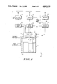
- FIG. 1 is a block diagram of a memory according to a preferred of the invention.
- FIG. 2 is a circuit diagram of a first portion of the memory of FIG. 1;
- FIG. 3 is a circuit diagram of a second portion of the memory of FIG. 1;
- FIG. 4 is a timing diagram of signals present in the memory of FIG. 1.
- FIG. 1 Shown in FIG. 1 is a memory 10 comprised of an array 11, a row decoder 12, a column decoder 13, data lines 14, a data-in buffer 15, a write enable buffer 16, a data-out buffer 17, a write driver 18, a transition detector 19, a pulse control circuit 21, and a sense amplifier 22.
- Buffer 16 receives an externally provided write enable signal *WE which is active at a logic low and thus indicates that memory 10 is to be in a write mode when it is a logic low.
- the asterisk (*) in front of the signal designation indicates that the signal is active at a logic low.
- Signal *WE at a logic high indicates that memory 10 is in a read mode.
- Buffer 16 outputs a first write enable signal WE1 and a second write enable signal WE2 responsive to signal *WE for use by pulse control circuit 21 and buffer 17, respectively.
- the operation of memory 10 is described in two modes, the read mode and the write mode.
- signal *WE is a logic high
- buffer 17 outputs a data-out signal DO representative of a logic state stored in a memory cell selected by a column address and a row address.
- Row decoder 12 selects a word line in array 11 as determined by the row address. All of the memory cells coupled to the selected word line are enabled.
- the memory cells in array 11 are coupled to word lines and bit line pairs at intersections thereof. When enabled, a memory cell either outputs data onto the bit line pair to which it is coupled or receives data from the bit line pair to which it is coupled.
- a selected memory cell outputs data onto the bit line pair to which it is coupled.
- Column decoder selects a bit line pair in response to a column address.
- Column decoder 13 accomplishes the selection by coupling the selected bit line pair to data lines 14.
- Sense amplifier 22 senses the logic state provided onto data lines 14 and outputs it to buffer 17 which in turn outputs signal DO in response to the logic state provided by sense amplifier 22.
- the selection of a cell is accomplished in the same manner as in the read mode.
- a selected bit line pair is driven to a logic state by virtue of data lines 14 being driven to a logic state by write driver 18.
- Write driver 18 drives data lines 14 to a logic state representative of the logic state of data-in signal DI received by buffer 15.
- Buffer 15 provides an output to write driver 18 representative of the logic state of signal DI.
- the selected bit line pair is coupled to data lines 14 so the selected bit line pair is driven to the logic state representative of the logic state of signal DI.
- the particular approach taken for the duration of a write is a timed write approach in which write driver is active for a duration defined by an internal write driver enable pulse WDE.
- Pulse control circuit 21 provides pulse WDE to write driver 18 responsive to signal WE1 and a pulse *DT.
- Pulse WDE is generated for a predetermined length of time, for example, 5 nanoseconds (ns), in response to either a transition of signal WE1 from a logic low to a logic high or a transition of signal DI while signal WE1 is a logic high. Pulse WDE is thus generated upon entry into the write mode and may also be again generated during the write mode if there is a data change during the write mode.
- Transition detector 19, coupled to buffer 15, detects a change in signal DI and provides data transition pulse *DT if there is a data change. Pulse WDE is also provided to data lines 14 for charging data lines 14 when write driver 18 is inactive.
- Pulse control circuit 21 also provides a late data-transition pulse LDT to data lines 14 for high speed charging of data lines 14 for the case in which there is a data change near the end of the write mode. Pulses WDE and LDT are provided to data lines 14 for write recovery of data lines 14 and the selected bit line pair.
- FIG. 2 Shown in FIG. 2 is portion of array 11, column decoder 13, and data lines 14.
- the portion of array 11 shown in FIG. 2 comprises a bit line pair 26 comprised of a bit line 27 and a bit line 28, a bit line pair 29 comprised of a bit line 31 and a bit line 32, a word line 33, a word line 34, a memory cell 36 coupled to word line 33 and bit lines 27 and 28, a memory cell 37 coupled to word line 33 and bit lines 31 and 32, a memory cell 38 coupled to word line 34 and bit lines 27 and 28, a memory cell 39 coupled to word line 34 and bit lines 31 and 32, a diode-connected N channel transistor 41 connected between a positive power supply terminal VDD and bit line 27, a diode-connected N channel transistor 42 connected between VDD and bit line 28, a diode-connected N channel transistor 43 connected between VDD and bit line 31, and a diode-connected N channel transistor 44 connected between VDD and bit line 32.
- a diode-connected N channel transistor 41 connected between
- Data lines 14 comprises a data line pair 46 comprised of a data line 47 and a data line 48, a P channel transistor 51, a P channel transistor 52, an NPN transistor 53, and an NPN transistor 54.
- the portion of column decoder shown in FIG. 2 comprises an N channel transistor 56, an N channel transistor 57, an N channel transistor 58, and an N channel transistor 59.
- Transistor 51 has a source connected to VDD, a gate for receiving pulse WDE, and a drain connected to data line 47.
- Transistor 52 has a source connected to VDD, a gate for receiving pulse WDE, and a drain connected to data line 48.
- Transistor 53 has a collector connected to VDD, a base for receiving pulse LDT, and an emitter connected to data line 47.
- Transistor 54 has a collector connected to VDD, a base for receiving pulse LDT, and an emitter connected to data line 48.
- Transistor 56 which uses the bilateral characteristic of MOS-type transistors, has a first current electrode connected to data line 47, a second current electrode connected to bit line 27, and a control electrode for receiving a column decoder signal CD1.
- Transistor 57 has a first current electrode connected to data line 48, a second current electrode connected to bit line 28, and a control electrode for receiving signal CD1.
- Transistor 58 has a first current electrode coupled to data line 47, a second current electrode coupled to bit line 31, and a control electrode for receiving column decoder signal CDN.
- Transistor 59 has a first current electrode connected to a data line 48, a second current electrode coupled to bit line 32, and a gate for receiving signal CDN.
- pulse WDE When write driver 18 is active in driving data line pair 46, pulse WDE has pulsed to a logic high so that transistors 51 and 52 are non-conductive. When pulse WDE is inactive it is a logic low so that transistors 51 and 52 are conductive when memory 10 is not in the write mode.
- pulse LDT may be generated. If pulse LDT is generated, transistors 53 and 54 are conductive. Pulse LDT is generated only if the WDE pulse is extended beyond the termination of external signal *WE. This is the case in which write recovery must be most rapid because the termination of the write mode is the beginning of the read mode. Data line pair 46 and the selected bit line pair must be charged back to the precharge voltage prior to sensing. Thus, transistors 53 and 54 are enabled for the case where the actual writing occurs beyond the external termination of the write mode.
- pulse control circuit 21 which comprises an inverter 61, a transmission gate 62, a P channel transistor 64, a NAND gate 65, a NAND gate 66, an inverter 67, a NOR gate 68, a delay circuit 69, and a delay circuit 70.
- Inverter 61 has an input for receiving signal WE1, and an output.
- Delay circuit 70 has an input connected to the output of inverter 61, and an output.
- NAND gate 65 has a first input connected to the output of delay circuit 70, a second input for receiving signal WE1, and an output.
- Inverter 63 has an input for receiving signal WE1, and an output.
- Transmission gate 62 has a signal input for receiving pulse *DT, a true control input for receiving signal WE1, a complementary control input connected to the output of inverter 63, and a data output.
- Transistor 64 has a gate for receiving signal WE1, a source connected to VDD, and a drain connected to the data output of transmission gate 62.
- NAND gate 66 has a first input connected to the output of NAND gate 65, a second input connected to the data output of transmission gate 62, and an output for providing pulse WDE.
- Inverter 67 has an input connected to the output of NAND gate 66, and an output.
- NOR gate 68 has a first input connected to the output of inverter 67, a second input for receiving signal WE1, and an output.
- Delay circuit 69 has an input connected to the output of NOR gate 68, and an output for providing pulse LDT.
- signal WE1 is a logic low so that transmission gate 62 is non-conductive, transistor 64 is conductive, and NAND gate 65 is forced to provide a logic high output.
- NAND gate 66 thus has a logic high on both inputs causing NAND gate 66 to provide pulse WDE at a logic low.
- inverter 67 With the output of NAND gate 66 at a logic low, inverter 67 outputs a logic high which forces NOR gate 68 to output a logic low which causes delay circuit 69 to output pulse LDT at a logic low.
- pulses LDT and WDE are at a steady state logic low.
- NAND gate 65 Upon a transition of signal WE1 to a logic high which is caused by external signal *WE switching from a logic high to a logic low, NAND gate 65 will respond by providing a logic low output. Inverter 61 and delay circuit 70 cause a delay in the transition of signal WE1 reaching NAND gate 65. Thus upon the transition of signal WE1 switching to a logic high, both inputs of NAND gate 65 are temporarily a logic high so that NAND gate 65 outputs a logic low. The logic low output of NAND gate 65 forces NAND gate 66 to provide pulse WDE at a logic high. This responsiveness of pulse WDE to signal WE1 is shown in FIG. 4.
- Pulse *DT is a logic high except for a predetermined time duration following a transition of data-in signal DI. While signal WE1 is a logic high, transmission gate 62 couples pulse *DT to NAND gate 66. So long as there is no data change while signal WE1 is a logic high, NAND gate 66 will be responsive to the output of NAND gate 65. For a data change after signal WE1 has switched to a logic high, pulse *DT will pulse to a logic low which will force NAND gate 66 to output pulse WDE at a logic high. Inverter 67 will then output a logic low to NOR gate 68. For the case in which signal WE1 remains at a logic low, pulse WDE will remain at a logic high for the duration of pulse *DT at a logic low.
- inverter 67 will switch back to a logic high.
- the more difficult case, however, is when signal WE1 switches to a logic low the specified minimum time following a data change. This specified minimum time is commonly known as the time from data valid to write high (DVWH).
- signal WE1 switches to a logic low while pulse *DT is a logic low, pulse WDE is a logic high, and the output of inverter 67 is a logic low.
- Both inputs of NOR gate 68 are then at a logic low which causes the output of NOR gate 68 to switch to a logic high.
- Pulse LDT then switches to a logic high a delay time determined by delay circuit 69 after the output of NOR gate 68 switches to a logic high.
- Pulse WE1 switching to a logic low causes transmission gate to become nonconductive and P channel transistor to provide a logic high to NAND gate 66 and thus terminating pulse WDE.
- the delay time between the transition of signal WE1 and the termination of pulse WDE plus the specified delay between a data transition and the termination of the write mode is sufficient for write driver 18 to perform the required write.
- Pulse LDT at a logic high enables transistors 53 and 54 to precharge data lines 47 and 48 and the selected bit line pair to the necessary level as required to perform the subsequent read.
- the duration of pulse LDT is set by the delay from signal WE1 switching to a logic low and the output of inverter 67 switching to a logic high.
- the pulse width of pulse LDT can be relatively short because bipolar transistors 53 and 54 can couple charge very rapidly.
- the delay of delay circuit 69 ensures that pulse LDT will not occur until write driver 18 is disabled. Precharging of data lines 14 does occur in response to a data transition which occurs during the write mode in response to pulse LDT. Pulse LDT is suppressed, however, if signal WDE becomes inactive before signal WE1 switches to a logic low. Pulse LDT is not necessary in such a case because transistors 51 and 52 have enough time to provide the requisite precharging before the read begins.
- the WDE pulse is generated only for a logic low to logic high transition of signal WE1 or a data transition while signal WE1 is a logic high. While signal WE1 is a logic low, transmission gate 62 is non-conductive so that pulse *DT is decoupled from NAND gate 66. Furthermore, P channel transistor 64 provides a logic high to NAND gate 66 while signal WE1 is a logic low. For a logic high to logic low transition of signal WE1, NAND gates maintains a logic high output. Just prior to the transition, delay circuit 70 outputs a logic low to NAND gate 65. Upon the logic high to logic low, delay circuit 70 will provide a logic high output but only after NAND gate 65 has already received the logic low of signal WE1 so that NAND gate 65 maintains a logic high output during this transition.
- precharging the data lines in response to a data transition is useful for write recovery.
- There is a self-timed write which is used for the case in which the data is not changed during the write mode.
- This approach is known to have advantages for high speed applications. Flexibility is added by allowing data changes during the write mode. This is provided while still providing high speed operation by having a timed write following the detection of a data transition and further by enhancing the write recovery with a circuit which is also responsive to the data transition.
Landscapes
- Engineering & Computer Science (AREA)
- Microelectronics & Electronic Packaging (AREA)
- Computer Hardware Design (AREA)
- Static Random-Access Memory (AREA)
Abstract
Description
Claims (7)
Priority Applications (1)
| Application Number | Priority Date | Filing Date | Title |
|---|---|---|---|
| US07/128,559 US4802129A (en) | 1987-12-03 | 1987-12-03 | RAM with dual precharge circuit and write recovery circuitry |
Applications Claiming Priority (1)
| Application Number | Priority Date | Filing Date | Title |
|---|---|---|---|
| US07/128,559 US4802129A (en) | 1987-12-03 | 1987-12-03 | RAM with dual precharge circuit and write recovery circuitry |
Publications (1)
| Publication Number | Publication Date |
|---|---|
| US4802129A true US4802129A (en) | 1989-01-31 |
Family
ID=22435907
Family Applications (1)
| Application Number | Title | Priority Date | Filing Date |
|---|---|---|---|
| US07/128,559 Expired - Lifetime US4802129A (en) | 1987-12-03 | 1987-12-03 | RAM with dual precharge circuit and write recovery circuitry |
Country Status (1)
| Country | Link |
|---|---|
| US (1) | US4802129A (en) |
Cited By (27)
| Publication number | Priority date | Publication date | Assignee | Title |
|---|---|---|---|---|
| US4933905A (en) * | 1987-08-13 | 1990-06-12 | Kabushiki Kaisha Toshiba | Semiconductor memory device for reducing power dissipation during a write operation |
| US4945516A (en) * | 1987-10-09 | 1990-07-31 | Hitachi, Ltd. | Write control circuit for a high-speed memory device |
| US4947374A (en) * | 1987-05-12 | 1990-08-07 | Mitsubishi Denki Kabushiki Kaisha | Semiconductor memeory device in which writing is inhibited in address skew period and controlling method thereof |
| US4998222A (en) * | 1989-12-04 | 1991-03-05 | Nec Electronics Inc. | Dynamic random access memory with internally gated RAS |
| US5043945A (en) * | 1989-09-05 | 1991-08-27 | Motorola, Inc. | Memory with improved bit line and write data line equalization |
| FR2664080A1 (en) * | 1990-06-30 | 1992-01-03 | Samsung Electronics Co Ltd | Write control circuit having preload means |
| EP0490651A3 (en) * | 1990-12-13 | 1993-01-27 | Sgs-Thomson Microelectronics, Inc. (A Delaware Corp.) | A semiconductor memory with column equilibrate on change of date during a write cycle |
| US5229967A (en) * | 1990-09-04 | 1993-07-20 | Nogle Scott G | BICMOS sense circuit for sensing data during a read cycle of a memory |
| US5262995A (en) * | 1991-05-24 | 1993-11-16 | Samsung Electronics Co., Ltd. | Method for precharging imput/output lines of a memory device |
| EP0509811A3 (en) * | 1991-04-18 | 1993-12-08 | Mitsubishi Electric Corp | Semiconductor memory device |
| US5315555A (en) * | 1991-06-19 | 1994-05-24 | Samsung Electronics Co., Ltd. | Sense amplifier for performing a high-speed sensing operation |
| US5349560A (en) * | 1992-03-30 | 1994-09-20 | Samsung Electronics Co., Ltd. | Semiconductor memory device with improved bit line precharged circuits |
| US5416744A (en) * | 1994-03-08 | 1995-05-16 | Motorola Inc. | Memory having bit line load with automatic bit line precharge and equalization |
| US5418749A (en) * | 1992-11-18 | 1995-05-23 | Nec Corporation | Semiconductor memory device |
| US5574866A (en) * | 1993-04-05 | 1996-11-12 | Zenith Data Systems Corporation | Method and apparatus for providing a data write signal with a programmable duration |
| US5602785A (en) * | 1995-12-13 | 1997-02-11 | Micron Technology, Inc. | P-channel sense amplifier pull-up circuit with a timed pulse for use in DRAM memories having non-bootstrapped word lines |
| US5732036A (en) * | 1997-02-14 | 1998-03-24 | Micron Technology, Inc. | Memory device communication line control |
| US5781469A (en) * | 1997-01-24 | 1998-07-14 | Atmel Corporation | Bitline load and precharge structure for an SRAM memory |
| US5781501A (en) * | 1996-06-27 | 1998-07-14 | Hyundai Electronics Industries Co., Ltd. | Circuit and method for securing write recovery operation in a synchronous semiconductor memory device |
| EP0774757A3 (en) * | 1995-11-03 | 1999-05-26 | Samsung Electronics Co., Ltd. | Precharge circuit for a semiconductor memory device |
| US6154404A (en) * | 1998-07-23 | 2000-11-28 | Samsung Electronics Co., Ltd. | Integrated circuit memory devices having sense amplifier driver circuits therein that improve writing efficiency |
| US20040109366A1 (en) * | 2002-12-04 | 2004-06-10 | Jang-Won Moon | Variable-delay precharge circuits and methods |
| US20100157715A1 (en) * | 2008-12-18 | 2010-06-24 | Hong-Beom Pyeon | Semiconductor device with main memory unit and auxiliary memory unit requiring preset operation |
| US20100161877A1 (en) * | 2008-12-18 | 2010-06-24 | Hong Beom Pyeon | Device and method for transferring data to a non-volatile memory device |
| US20110032784A1 (en) * | 2009-08-05 | 2011-02-10 | Hong-Beom Pyeon | Semiconductor memory with multiple wordline selection |
| EP3567591A1 (en) * | 2017-05-04 | 2019-11-13 | Tang, Chao-Jing | Random-access memory and associated circuit, method and device |
| US10839875B2 (en) | 2019-03-29 | 2020-11-17 | Advanced Micro Devices, Inc. | Timer for use dual voltage supplies |
Citations (3)
| Publication number | Priority date | Publication date | Assignee | Title |
|---|---|---|---|---|
| JPS59221891A (en) * | 1983-05-31 | 1984-12-13 | Toshiba Corp | Static semiconductor storage device |
| US4712197A (en) * | 1986-01-28 | 1987-12-08 | Motorola, Inc. | High speed equalization in a memory |
| US4722074A (en) * | 1984-10-31 | 1988-01-26 | Mitsubishi Denki Kabushiki Kaisha | Semiconductor storage unit with I/O bus precharging and equalization |
-
1987
- 1987-12-03 US US07/128,559 patent/US4802129A/en not_active Expired - Lifetime
Patent Citations (3)
| Publication number | Priority date | Publication date | Assignee | Title |
|---|---|---|---|---|
| JPS59221891A (en) * | 1983-05-31 | 1984-12-13 | Toshiba Corp | Static semiconductor storage device |
| US4722074A (en) * | 1984-10-31 | 1988-01-26 | Mitsubishi Denki Kabushiki Kaisha | Semiconductor storage unit with I/O bus precharging and equalization |
| US4712197A (en) * | 1986-01-28 | 1987-12-08 | Motorola, Inc. | High speed equalization in a memory |
Cited By (47)
| Publication number | Priority date | Publication date | Assignee | Title |
|---|---|---|---|---|
| US4947374A (en) * | 1987-05-12 | 1990-08-07 | Mitsubishi Denki Kabushiki Kaisha | Semiconductor memeory device in which writing is inhibited in address skew period and controlling method thereof |
| US4933905A (en) * | 1987-08-13 | 1990-06-12 | Kabushiki Kaisha Toshiba | Semiconductor memory device for reducing power dissipation during a write operation |
| US4945516A (en) * | 1987-10-09 | 1990-07-31 | Hitachi, Ltd. | Write control circuit for a high-speed memory device |
| US5043945A (en) * | 1989-09-05 | 1991-08-27 | Motorola, Inc. | Memory with improved bit line and write data line equalization |
| US4998222A (en) * | 1989-12-04 | 1991-03-05 | Nec Electronics Inc. | Dynamic random access memory with internally gated RAS |
| FR2664080A1 (en) * | 1990-06-30 | 1992-01-03 | Samsung Electronics Co Ltd | Write control circuit having preload means |
| GB2245730A (en) * | 1990-06-30 | 1992-01-08 | Samsung Electronics Co Ltd | Memory write driver timing generator with precharge pulse for rapid write to read transition |
| GB2245730B (en) * | 1990-06-30 | 1994-08-10 | Samsung Electronics Co Ltd | A write driver having a precharging means |
| US5229967A (en) * | 1990-09-04 | 1993-07-20 | Nogle Scott G | BICMOS sense circuit for sensing data during a read cycle of a memory |
| US5305268A (en) * | 1990-12-13 | 1994-04-19 | Sgs-Thomson Microelectronics, Inc. | Semiconductor memory with column equilibrate on change of data during a write cycle |
| EP0490651A3 (en) * | 1990-12-13 | 1993-01-27 | Sgs-Thomson Microelectronics, Inc. (A Delaware Corp.) | A semiconductor memory with column equilibrate on change of date during a write cycle |
| US5623454A (en) * | 1991-04-18 | 1997-04-22 | Mitsubishi Denki Kabushiki Kaisha | Semiconductor memory device |
| US6356484B2 (en) | 1991-04-18 | 2002-03-12 | Mitsubishi Denki Kabushiki Kaisha | Semiconductor memory device |
| EP0509811A3 (en) * | 1991-04-18 | 1993-12-08 | Mitsubishi Electric Corp | Semiconductor memory device |
| US6026029A (en) * | 1991-04-18 | 2000-02-15 | Mitsubishi Denki Kabushiki Kaisha | Semiconductor memory device |
| US5848004A (en) * | 1991-04-18 | 1998-12-08 | Mitsubishi Denki Kabushiki Kaisha | Semiconductor memory device |
| EP0817198A1 (en) * | 1991-04-18 | 1998-01-07 | Mitsubishi Denki Kabushiki Kaisha | Semiconductor memory device |
| US5544121A (en) * | 1991-04-18 | 1996-08-06 | Mitsubishi Denki Kabushiki Kaisha | Semiconductor memory device |
| US5559750A (en) * | 1991-04-18 | 1996-09-24 | Mitsubishi Denki Kabushiki Kaisha | Semiconductor memory device |
| US5652723A (en) * | 1991-04-18 | 1997-07-29 | Mitsubishi Denki Kabushiki Kaisha | Semiconductor memory device |
| US5583813A (en) * | 1991-04-18 | 1996-12-10 | Mitsubishi Denki Kabushiki Kaisha | Semiconductor memory device |
| US5650968A (en) * | 1991-04-18 | 1997-07-22 | Mitsubishi Denki Kabushiki Kaisha | Semiconductor memory device |
| US5629895A (en) * | 1991-04-18 | 1997-05-13 | Mitsubishi Electric Engineering Co., Ltd. | Semiconductor memory device |
| US5262995A (en) * | 1991-05-24 | 1993-11-16 | Samsung Electronics Co., Ltd. | Method for precharging imput/output lines of a memory device |
| US5315555A (en) * | 1991-06-19 | 1994-05-24 | Samsung Electronics Co., Ltd. | Sense amplifier for performing a high-speed sensing operation |
| US5349560A (en) * | 1992-03-30 | 1994-09-20 | Samsung Electronics Co., Ltd. | Semiconductor memory device with improved bit line precharged circuits |
| US5418749A (en) * | 1992-11-18 | 1995-05-23 | Nec Corporation | Semiconductor memory device |
| US5574866A (en) * | 1993-04-05 | 1996-11-12 | Zenith Data Systems Corporation | Method and apparatus for providing a data write signal with a programmable duration |
| US5416744A (en) * | 1994-03-08 | 1995-05-16 | Motorola Inc. | Memory having bit line load with automatic bit line precharge and equalization |
| EP0774757A3 (en) * | 1995-11-03 | 1999-05-26 | Samsung Electronics Co., Ltd. | Precharge circuit for a semiconductor memory device |
| US5602785A (en) * | 1995-12-13 | 1997-02-11 | Micron Technology, Inc. | P-channel sense amplifier pull-up circuit with a timed pulse for use in DRAM memories having non-bootstrapped word lines |
| US5781501A (en) * | 1996-06-27 | 1998-07-14 | Hyundai Electronics Industries Co., Ltd. | Circuit and method for securing write recovery operation in a synchronous semiconductor memory device |
| US5781469A (en) * | 1997-01-24 | 1998-07-14 | Atmel Corporation | Bitline load and precharge structure for an SRAM memory |
| EP0960421A1 (en) | 1997-01-24 | 1999-12-01 | Atmel Corporation | Bitline load and precharge structure for an sram memory |
| US5963493A (en) * | 1997-02-14 | 1999-10-05 | Micron Technology, Inc. | Memory device communication line control |
| US5875140A (en) * | 1997-02-14 | 1999-02-23 | Micron Technology, Inc. | Memory device communication line control |
| US5732036A (en) * | 1997-02-14 | 1998-03-24 | Micron Technology, Inc. | Memory device communication line control |
| US6154404A (en) * | 1998-07-23 | 2000-11-28 | Samsung Electronics Co., Ltd. | Integrated circuit memory devices having sense amplifier driver circuits therein that improve writing efficiency |
| US20040109366A1 (en) * | 2002-12-04 | 2004-06-10 | Jang-Won Moon | Variable-delay precharge circuits and methods |
| US20100157715A1 (en) * | 2008-12-18 | 2010-06-24 | Hong-Beom Pyeon | Semiconductor device with main memory unit and auxiliary memory unit requiring preset operation |
| US20100161877A1 (en) * | 2008-12-18 | 2010-06-24 | Hong Beom Pyeon | Device and method for transferring data to a non-volatile memory device |
| US8037235B2 (en) | 2008-12-18 | 2011-10-11 | Mosaid Technologies Incorporated | Device and method for transferring data to a non-volatile memory device |
| US8194481B2 (en) | 2008-12-18 | 2012-06-05 | Mosaid Technologies Incorporated | Semiconductor device with main memory unit and auxiliary memory unit requiring preset operation |
| US20110032784A1 (en) * | 2009-08-05 | 2011-02-10 | Hong-Beom Pyeon | Semiconductor memory with multiple wordline selection |
| US8068382B2 (en) | 2009-08-05 | 2011-11-29 | Mosaid Technologies Incorporated | Semiconductor memory with multiple wordline selection |
| EP3567591A1 (en) * | 2017-05-04 | 2019-11-13 | Tang, Chao-Jing | Random-access memory and associated circuit, method and device |
| US10839875B2 (en) | 2019-03-29 | 2020-11-17 | Advanced Micro Devices, Inc. | Timer for use dual voltage supplies |
Similar Documents
| Publication | Publication Date | Title |
|---|---|---|
| US4802129A (en) | RAM with dual precharge circuit and write recovery circuitry | |
| US4355377A (en) | Asynchronously equillibrated and pre-charged static ram | |
| US4417328A (en) | Random access semiconductor memory device using MOS transistors | |
| EP0330852B1 (en) | Decoder/driver circuit for semiconductor memories | |
| US5508644A (en) | Sense amplifier for differential voltage detection with low input capacitance | |
| US5091885A (en) | Dynamic type random-access memory having improved timing characteristics | |
| US4542483A (en) | Dual stage sense amplifier for dynamic random access memory | |
| US5777935A (en) | Memory device with fast write recovery and related write recovery method | |
| KR920013447A (en) | Semiconductor memory having columns that equalize as data changes during a write cycle | |
| US4751680A (en) | Bit line equalization in a memory | |
| KR940006994B1 (en) | Dynamic random access memory and method for writing data thereto | |
| US4712197A (en) | High speed equalization in a memory | |
| US4638462A (en) | Self-timed precharge circuit | |
| GB2226900A (en) | Memory timing circuit | |
| EP0096421A2 (en) | Static memory device with signal transition detector | |
| US4712194A (en) | Static random access memory | |
| US4110840A (en) | Sense line charging system for random access memory | |
| US5748556A (en) | Tristatable driver for internal data bus lines | |
| US4689771A (en) | Memory with improved write mode to read mode transition | |
| US4131951A (en) | High speed complementary MOS memory | |
| EP0547890A2 (en) | A read/write memory with interlocked write control | |
| EP0259862A1 (en) | Semiconductor memory with improved write function | |
| US4706218A (en) | Memory input buffer with hysteresis | |
| US6067264A (en) | High speed semiconductor memory device | |
| US4764900A (en) | High speed write technique for a memory |
Legal Events
| Date | Code | Title | Description |
|---|---|---|---|
| AS | Assignment |
Owner name: MOTOROLA, INC., SCHAUMBURG, ILLINOIS, A CORP. OF D Free format text: ASSIGNMENT OF ASSIGNORS INTEREST.;ASSIGNORS:HOEKSTRA, GEORGE P.;PELLEY, PERRY H. III;REEL/FRAME:004798/0452 Effective date: 19871117 Owner name: MOTOROLA, INC., SCHAUMBURG, ILLINOIS, A CORP. OF,D Free format text: ASSIGNMENT OF ASSIGNORS INTEREST;ASSIGNORS:HOEKSTRA, GEORGE P.;PELLEY, PERRY H. III;REEL/FRAME:004798/0452 Effective date: 19871117 |
|
| STCF | Information on status: patent grant |
Free format text: PATENTED CASE |
|
| CC | Certificate of correction | ||
| FPAY | Fee payment |
Year of fee payment: 4 |
|
| FPAY | Fee payment |
Year of fee payment: 8 |
|
| FPAY | Fee payment |
Year of fee payment: 12 |
|
| AS | Assignment |
Owner name: FREESCALE SEMICONDUCTOR, INC., TEXAS Free format text: ASSIGNMENT OF ASSIGNORS INTEREST;ASSIGNOR:MOTOROLA, INC.;REEL/FRAME:015698/0657 Effective date: 20040404 Owner name: FREESCALE SEMICONDUCTOR, INC.,TEXAS Free format text: ASSIGNMENT OF ASSIGNORS INTEREST;ASSIGNOR:MOTOROLA, INC.;REEL/FRAME:015698/0657 Effective date: 20040404 |
|
| AS | Assignment |
Owner name: CITIBANK, N.A. AS COLLATERAL AGENT, NEW YORK Free format text: SECURITY AGREEMENT;ASSIGNORS:FREESCALE SEMICONDUCTOR, INC.;FREESCALE ACQUISITION CORPORATION;FREESCALE ACQUISITION HOLDINGS CORP.;AND OTHERS;REEL/FRAME:018855/0129 Effective date: 20061201 Owner name: CITIBANK, N.A. AS COLLATERAL AGENT,NEW YORK Free format text: SECURITY AGREEMENT;ASSIGNORS:FREESCALE SEMICONDUCTOR, INC.;FREESCALE ACQUISITION CORPORATION;FREESCALE ACQUISITION HOLDINGS CORP.;AND OTHERS;REEL/FRAME:018855/0129 Effective date: 20061201 |
|
| AS | Assignment |
Owner name: FREESCALE SEMICONDUCTOR, INC., TEXAS Free format text: PATENT RELEASE;ASSIGNOR:CITIBANK, N.A., AS COLLATERAL AGENT;REEL/FRAME:037354/0225 Effective date: 20151207 |