US4797577A - Bandgap reference circuit having higher-order temperature compensation - Google Patents
Bandgap reference circuit having higher-order temperature compensation Download PDFInfo
- Publication number
- US4797577A US4797577A US07/133,778 US13377887A US4797577A US 4797577 A US4797577 A US 4797577A US 13377887 A US13377887 A US 13377887A US 4797577 A US4797577 A US 4797577A
- Authority
- US
- United States
- Prior art keywords
- transistor
- transistors
- emitter
- coupled
- circuit
- Prior art date
- Legal status (The legal status is an assumption and is not a legal conclusion. Google has not performed a legal analysis and makes no representation as to the accuracy of the status listed.)
- Expired - Lifetime
Links
Images
Classifications
-
- G—PHYSICS
- G05—CONTROLLING; REGULATING
- G05F—SYSTEMS FOR REGULATING ELECTRIC OR MAGNETIC VARIABLES
- G05F3/00—Non-retroactive systems for regulating electric variables by using an uncontrolled element, or an uncontrolled combination of elements, such element or such combination having self-regulating properties
- G05F3/02—Regulating voltage or current
- G05F3/08—Regulating voltage or current wherein the variable is dc
- G05F3/10—Regulating voltage or current wherein the variable is dc using uncontrolled devices with non-linear characteristics
- G05F3/16—Regulating voltage or current wherein the variable is dc using uncontrolled devices with non-linear characteristics being semiconductor devices
- G05F3/20—Regulating voltage or current wherein the variable is dc using uncontrolled devices with non-linear characteristics being semiconductor devices using diode- transistor combinations
- G05F3/30—Regulators using the difference between the base-emitter voltages of two bipolar transistors operating at different current densities
-
- Y—GENERAL TAGGING OF NEW TECHNOLOGICAL DEVELOPMENTS; GENERAL TAGGING OF CROSS-SECTIONAL TECHNOLOGIES SPANNING OVER SEVERAL SECTIONS OF THE IPC; TECHNICAL SUBJECTS COVERED BY FORMER USPC CROSS-REFERENCE ART COLLECTIONS [XRACs] AND DIGESTS
- Y10—TECHNICAL SUBJECTS COVERED BY FORMER USPC
- Y10S—TECHNICAL SUBJECTS COVERED BY FORMER USPC CROSS-REFERENCE ART COLLECTIONS [XRACs] AND DIGESTS
- Y10S323/00—Electricity: power supply or regulation systems
- Y10S323/907—Temperature compensation of semiconductor
Definitions
- This invention relates to a bandgap reference circuit for providing a reference voltage.
- a known bandgap reference circuit comprises first and second transistors, the second of which has an emitter area N times that of the first transistor.
- the two transistors are arranged to pass equal currents, the emitter of the second transistor being coupled to ground reference potential through two series connected resistors, whilst the emitter of the first transistor is coupled to the junction of the two resistors.
- the bases of the two transistors are coupled together and to an output terminal at which the output reference voltage is provided.
- the known circuit provides correction for the linear variation with temperature of the base-emitter voltage of the first transistor by the provision of the second transistor together with the two series connected resistors, the ratio of the values of the two resistors being chosen to correct the first derivative of the base-emitter voltage with respect to temperature.
- This invention seeks to provide an improved bandgap reference circuit in which the above problem is mitigated.
- a bandgap reference circuit comprising first and second transistors arranged in parallel to share a current, each having a first, second and control electrode, the control electrodes of the transistors being coupled together and to an output terminal; first and second resistors connected in series between the first electrode of the second transistor and a reference potential, the first electrode of the first transistor being coupled to a first node between the resistors; a third transistor having a first electrode coupled to the said first node a second electrode coupled to the output terminal, and a control electrode; third and fourth resistors connected in series between the output terminal and the reference potential, the control electrode of the third transistor being coupled to a second node between the third and fourth resistors.
- the first electrodes of the first and second transistors are typically emitter electrodes.
- the emitter area of the second transistor is N times that of the first and the emitter area of the third transistor is M times that of the first.
- Negative feedback means may be provided for maintaining the output voltage substantially constant.
- a starting circuit may be provided for ensuring that the first and second transistors turn on when supply potential is applied to the circuit.
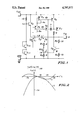
- FIG. 1 shows a preferred embodiment of the bandgap reference circuit of the invention
- FIG. 2 shows graphs of the variation of reference voltage with temperature for the prior art circuit and for the circuit of FIG. 1.
- the illustrated bandgap reference circuit comprises suppl terminals 1 and 2 which in operation are maintained at V cc and for example ground respectively.
- First and second NPN transistors T 1 and T 2 whose emitter areas are in the ratio 1 to N are connected in parallel to share equally a single current supplied from the supply terminal.
- the transistors T 1 and T 2 are fed to the transistors T 1 and T 2 from the supply terminal 1 via two PNP transistors T 3 and T 4 each having two collectors.
- the first collector 3a of the transistor T 3 is connected to the base of the same transistor to form a diode and also to the collector of the transistor T 1 .
- the second collector 3b is connected to the collector of the transistor T 2 .
- the transistor T 3 thus forms a current mirror.
- the transistor T 4 is also wired as a current mirror with first collector 4a being connected to the base electrode of transistor T 4 to form a diode, and also to the emitter of the transistor T 3 .
- the second collector 4b of the transistor T 4 is connected to the base electrode of a PNP transistor T 5 and to the emitter of a PNP transistor T 6 .
- the base of the transistor T 6 is connected to the collector 3b of the transistor T 3 , whilst the collector of transistor T 6 is connected to the ground reference terminal 2.
- the emitter of the transistor T 5 is connected to the supply terminal 1 and its collector to the base of a NPN transistor T 7 the collector of which is connected to the supply terminal 1 and whose emitter is connected to an output terminal 5.
- a resistor 6 has one terminal connected to the base of the transistor T 7 and a second terminal connected to the output terminal 5.
- a capacitor 7 has terminals connected respectively to the bases of the transistors T 6 and T 7 .
- the bases of the transistors T 1 and T 2 are connected together and to the output terminal 5.
- a pair of resistors 8 and 9 are connected in series between the emitter of the transistor T 2 and the ground terminal 2, the emitter of the transistor T 1 being connected to a first node 10 between the resistors.
- An NPN transistor T 8 with an emitter area M times that of the transistor T 1 has its emitter connected to the node 10, its collector connected to the output terminal 5 and its base connected to a second node 11 between a pair of resistors 12 and 13 connected in series between the output terminal 5 and the ground terminal 2.
- a transistor T 9 has its emitter connected to the bases of the transistors T 1 and T 2 and to the output terminal 5, its collector connected to the supply terminal 1 and its base connected to a third node 14 between a resistor 15 and two series connected transistors T 10 and T 11 which are each connected as diodes by the coupling together of their respective bases and collectors.
- the resistor 15 and the transistors T 10 and T 11 form a series connected voltage divider chain between the supply terminal 1 and the ground terminal 2.
- the transistors T 1 and T 2 are matched and a reference voltage V R will be provided at the output terminal 5 which depends on the base emitter voltage V BE of the transistor T 1 and upon temperature due to the variation of V BE with temperature.
- V R has a dependence upon temperature which has both linear and higher order components. From the analysis which follows it will be seen that by choice of the ratio of the values R 1 and R 2 of the resistors 8 and 9, the linear temperature dependent component may be compensated, whilst choice of the values R 3 and R 4 of the resistors 12 and 13 allows compensation of the quadratic dependence.
- the provision of the transistor T 8 which feeds its emitter current to the node 10, provides an additional degree of freedom to allow compensation of the second order curvature of the curve of reference voltage versus temperature.
- the current I o may be expressed as
- T absolute temperature
- resistors R 1 and R 2 , R 3 and R 4 are matched with a temperature coefficient ⁇ at a reference temperature T o , and that the respective values of the above mentioned resistors at T o are R 10 and R 20 , R 30 and R 40 then;
- transistors T 1 , T 2 and T 8 are also matched with T 2 and T 8 having above defined emitter areas N and M respectively times that of the transistor T 1 .
- V BE1 (T) is the base-emitter voltage of the transistor T 1 and n is an exponent, usually between 2 and 3 which depends upon the particular semiconductor process.
- V G (T) is the bandgap voltage which generally depends upon temperature.
- A is a constant which depends of process parameters and emitter area.
- the voltage V BE1 may be expressed as a function of temperature by taking the natural logarithm of the equation 4 as follows: ##EQU2##
- an offset also may occur due to the current gains of bipolar transistors which are generally limited.
- the circuit of the invention corrects this limitation.
- Negative feedback means is provided to maintain the output voltage V R constant. Indeed if V R decreases (or increases) the current through T 2 becomes larger (or smaller) than that through T 1 . By virtue of the action of the current mirror formed by the transistor T 3 , the difference of these currents will appear as base current of the transistor T 6 . This base current is increased (or decreased) and forces the transistors T 5 and T 7 to conduct more (or less) so that, the output voltage V R is forced to be increasing (or decreasing).
- the reference voltage V R When the circuit is first turned ⁇ on ⁇ , the reference voltage V R will be at about zero volts. To ensure that the transistors T 1 and T 2 turn on to establish the proper reference voltage, a starting circuit is provided by the transistor T 9 which is biased by the potential at node 14 of the potential divider chain formed by resistor 15 and the two diode connected transistors T 10 and T 11
- V cc When V cc is applied and the voltage at the node 14 rises more than one base-emitter voltage, the transistor T 9 will conduct, causing the voltage at the bases of the transistors T 1 and T 2 to rise, so tht T 1 and T 2 turn ⁇ on ⁇ . V R will then rise to its proper value.
- the node 14 cannot rise to a voltage more than 2V BE of the transistors T 10 and T 11 above ground potential. Since V R generally is approximately equal to this 2V BE value, the transistor T 9 will turn off when V R rises to a sufficient value to annul bias its base-emitter junction. The starting circuit then becomes inoperative.
- curve a a graph of the variation of the reference voltage with temperature for the circuit of this invention and at curve b the same graph plotted for a prior art bandgap reference circuit.
- the curves are self explanatory and clearly indicate the advantage of the circuit of the invention in providing quadratic law temperature correction which is not evident in the prior art circuit.
- the negative feedback loop formed by the transistors T 6 , T 4 , T 5 , T 7 resistor 6 and capacitor 7 may be simplified by omitting the transistors T 4 , T 6 and T 5 , resistor 6 and capacitor 7 and correcting the emitter of the transistor T 3 directly to the supply terminal 1 and the collector 3b directly to the base of the transistor T 7 and inverting the collectors of the transistors T 1 and T 2 .
- the negative feedback circuit may be omitted altogether and the emitter of the transistor T 3 connected directly to the supply terminal 1.
Abstract
Description
R.sub.1 I.sub.o =V.sub.T ln N 1.
V.sub.T =kT/q 2.
R.sub.1 /R.sub.10 =R.sub.2 /R.sub.20 =R.sub.3 /R.sub.30 =R.sub.4 /R.sub.40 1+αT.sub.o (T/T.sub.o -1) 3.
Claims (5)
Applications Claiming Priority (2)
| Application Number | Priority Date | Filing Date | Title |
|---|---|---|---|
| GB8630980 | 1986-12-29 | ||
| GB868630980A GB8630980D0 (en) | 1986-12-29 | 1986-12-29 | Bandgap reference circuit |
Publications (1)
| Publication Number | Publication Date |
|---|---|
| US4797577A true US4797577A (en) | 1989-01-10 |
Family
ID=10609640
Family Applications (1)
| Application Number | Title | Priority Date | Filing Date |
|---|---|---|---|
| US07/133,778 Expired - Lifetime US4797577A (en) | 1986-12-29 | 1987-12-14 | Bandgap reference circuit having higher-order temperature compensation |
Country Status (3)
| Country | Link |
|---|---|
| US (1) | US4797577A (en) |
| GB (2) | GB8630980D0 (en) |
| HK (1) | HK73093A (en) |
Cited By (23)
| Publication number | Priority date | Publication date | Assignee | Title |
|---|---|---|---|---|
| US4931718A (en) * | 1988-09-26 | 1990-06-05 | Siemens Aktiengesellschaft | CMOS voltage reference |
| US4954769A (en) * | 1989-02-08 | 1990-09-04 | Burr-Brown Corporation | CMOS voltage reference and buffer circuit |
| US4990846A (en) * | 1990-03-26 | 1991-02-05 | Delco Electronics Corporation | Temperature compensated voltage reference circuit |
| US5001414A (en) * | 1988-11-23 | 1991-03-19 | Thomson Microelectronics | Voltage reference circuit with linearized temperature behavior |
| US5004986A (en) * | 1989-10-02 | 1991-04-02 | Advanced Micro Devices, Inc. | Op-amp with internally generated bias and precision voltage reference using same |
| US5053640A (en) * | 1989-10-25 | 1991-10-01 | Silicon General, Inc. | Bandgap voltage reference circuit |
| US5146152A (en) * | 1991-06-12 | 1992-09-08 | Samsung Electronics Co., Ltd. | Circuit for generating internal supply voltage |
| US5198747A (en) * | 1990-05-02 | 1993-03-30 | Texas Instruments Incorporated | Liquid crystal display driver and driver method |
| US5258702A (en) * | 1989-04-01 | 1993-11-02 | Robert Bosch Gmbh | Precision reference voltage source |
| US5453712A (en) * | 1995-01-25 | 1995-09-26 | Honeywell Inc. | Circuit for accurately discharging a capacitor |
| US5519354A (en) * | 1995-06-05 | 1996-05-21 | Analog Devices, Inc. | Integrated circuit temperature sensor with a programmable offset |
| US5570008A (en) * | 1993-04-14 | 1996-10-29 | Texas Instruments Deutschland Gmbh | Band gap reference voltage source |
| US5719522A (en) * | 1992-12-11 | 1998-02-17 | Nippondenso Co., Ltd. | Reference voltage generating circuit having reduced current consumption with varying loads |
| US5814980A (en) * | 1996-09-03 | 1998-09-29 | International Business Machines Corporation | Wide range voltage regulator |
| US6535053B2 (en) | 2000-03-10 | 2003-03-18 | Austria Mikro Systeme International Aktiengesellschaft | Method for obtaining a temperature—independent voltage reference as well as a circuit arrangement for obtaining such a voltage reference |
| US6774711B2 (en) | 2002-11-15 | 2004-08-10 | Atmel Corporation | Low power bandgap voltage reference circuit |
| US20090096438A1 (en) * | 2007-10-10 | 2009-04-16 | Kazuhiko Yamada | Voltage control circuit |
| US20100046580A1 (en) * | 2008-08-20 | 2010-02-25 | Sanyo Electric Co., Ltd. | Temperature sensor circuit |
| US20130328615A1 (en) * | 2012-06-07 | 2013-12-12 | Renesas Electronics Corporation | Semiconductor dev ice having voltage generation circuit |
| DE19804747B4 (en) * | 1997-03-18 | 2016-02-04 | Tessera Advanced Technologies, Inc. (N. D. Ges. D. Staates Delaware) | Bandgap reference circuit and method |
| CN108052150A (en) * | 2017-12-14 | 2018-05-18 | 上海艾为电子技术股份有限公司 | A kind of bandgap voltage reference with source compensated by using high-order curvature |
| CN108536210A (en) * | 2018-07-10 | 2018-09-14 | 成都信息工程大学 | A kind of smoothed temperature compensation band gap reference source circuit |
| TWI662790B (en) * | 2014-12-05 | 2019-06-11 | 韓商愛思開海力士有限公司 | Buffer circuit capable of improving amplification performance |
Families Citing this family (5)
| Publication number | Priority date | Publication date | Assignee | Title |
|---|---|---|---|---|
| US4939442A (en) * | 1989-03-30 | 1990-07-03 | Texas Instruments Incorporated | Bandgap voltage reference and method with further temperature correction |
| DE4344447B4 (en) * | 1993-12-24 | 2009-04-02 | Atmel Germany Gmbh | Constant current source |
| US6084388A (en) * | 1998-09-30 | 2000-07-04 | Infineon Technologies Corporation | System and method for low power start-up circuit for bandgap voltage reference |
| JP5839953B2 (en) * | 2011-11-16 | 2016-01-06 | ルネサスエレクトロニクス株式会社 | Bandgap reference circuit and power supply circuit |
| CN102591394B (en) * | 2012-02-24 | 2013-11-06 | 电子科技大学 | Bandgap reference voltage source |
Citations (9)
| Publication number | Priority date | Publication date | Assignee | Title |
|---|---|---|---|---|
| US4263519A (en) * | 1979-06-28 | 1981-04-21 | Rca Corporation | Bandgap reference |
| US4396883A (en) * | 1981-12-23 | 1983-08-02 | International Business Machines Corporation | Bandgap reference voltage generator |
| US4443753A (en) * | 1981-08-24 | 1984-04-17 | Advanced Micro Devices, Inc. | Second order temperature compensated band cap voltage reference |
| US4524318A (en) * | 1984-05-25 | 1985-06-18 | Burr-Brown Corporation | Band gap voltage reference circuit |
| US4626770A (en) * | 1985-07-31 | 1986-12-02 | Motorola, Inc. | NPN band gap voltage reference |
| US4636710A (en) * | 1985-10-15 | 1987-01-13 | Silvo Stanojevic | Stacked bandgap voltage reference |
| US4714872A (en) * | 1986-07-10 | 1987-12-22 | Tektronix, Inc. | Voltage reference for transistor constant-current source |
| US4751463A (en) * | 1987-06-01 | 1988-06-14 | Sprague Electric Company | Integrated voltage regulator circuit with transient voltage protection |
| US4763018A (en) * | 1986-02-07 | 1988-08-09 | Plessey Overseas Limited | Transistor constant bias circuits |
-
1986
- 1986-12-29 GB GB868630980A patent/GB8630980D0/en active Pending
-
1987
- 1987-12-04 GB GB8728487A patent/GB2199677B/en not_active Expired
- 1987-12-14 US US07/133,778 patent/US4797577A/en not_active Expired - Lifetime
-
1993
- 1993-07-22 HK HK730/93A patent/HK73093A/en not_active IP Right Cessation
Patent Citations (9)
| Publication number | Priority date | Publication date | Assignee | Title |
|---|---|---|---|---|
| US4263519A (en) * | 1979-06-28 | 1981-04-21 | Rca Corporation | Bandgap reference |
| US4443753A (en) * | 1981-08-24 | 1984-04-17 | Advanced Micro Devices, Inc. | Second order temperature compensated band cap voltage reference |
| US4396883A (en) * | 1981-12-23 | 1983-08-02 | International Business Machines Corporation | Bandgap reference voltage generator |
| US4524318A (en) * | 1984-05-25 | 1985-06-18 | Burr-Brown Corporation | Band gap voltage reference circuit |
| US4626770A (en) * | 1985-07-31 | 1986-12-02 | Motorola, Inc. | NPN band gap voltage reference |
| US4636710A (en) * | 1985-10-15 | 1987-01-13 | Silvo Stanojevic | Stacked bandgap voltage reference |
| US4763018A (en) * | 1986-02-07 | 1988-08-09 | Plessey Overseas Limited | Transistor constant bias circuits |
| US4714872A (en) * | 1986-07-10 | 1987-12-22 | Tektronix, Inc. | Voltage reference for transistor constant-current source |
| US4751463A (en) * | 1987-06-01 | 1988-06-14 | Sprague Electric Company | Integrated voltage regulator circuit with transient voltage protection |
Non-Patent Citations (2)
| Title |
|---|
| Chu et al, "A New Dimension to Monolithic Voltage Regulators", IEEE Trans. Broadcast. & Telev. Receivers (U.S.A.) vol. BTR-18, No 2, May 1972, pp. 73-76. |
| Chu et al, A New Dimension to Monolithic Voltage Regulators , IEEE Trans. Broadcast. & Telev. Receivers (U.S.A.) vol. BTR 18, No 2, May 1972, pp. 73 76. * |
Cited By (32)
| Publication number | Priority date | Publication date | Assignee | Title |
|---|---|---|---|---|
| US4931718A (en) * | 1988-09-26 | 1990-06-05 | Siemens Aktiengesellschaft | CMOS voltage reference |
| US5001414A (en) * | 1988-11-23 | 1991-03-19 | Thomson Microelectronics | Voltage reference circuit with linearized temperature behavior |
| US4954769A (en) * | 1989-02-08 | 1990-09-04 | Burr-Brown Corporation | CMOS voltage reference and buffer circuit |
| US5258702A (en) * | 1989-04-01 | 1993-11-02 | Robert Bosch Gmbh | Precision reference voltage source |
| US5004986A (en) * | 1989-10-02 | 1991-04-02 | Advanced Micro Devices, Inc. | Op-amp with internally generated bias and precision voltage reference using same |
| US5053640A (en) * | 1989-10-25 | 1991-10-01 | Silicon General, Inc. | Bandgap voltage reference circuit |
| US4990846A (en) * | 1990-03-26 | 1991-02-05 | Delco Electronics Corporation | Temperature compensated voltage reference circuit |
| US5198747A (en) * | 1990-05-02 | 1993-03-30 | Texas Instruments Incorporated | Liquid crystal display driver and driver method |
| US5146152A (en) * | 1991-06-12 | 1992-09-08 | Samsung Electronics Co., Ltd. | Circuit for generating internal supply voltage |
| US5719522A (en) * | 1992-12-11 | 1998-02-17 | Nippondenso Co., Ltd. | Reference voltage generating circuit having reduced current consumption with varying loads |
| US5570008A (en) * | 1993-04-14 | 1996-10-29 | Texas Instruments Deutschland Gmbh | Band gap reference voltage source |
| US5453712A (en) * | 1995-01-25 | 1995-09-26 | Honeywell Inc. | Circuit for accurately discharging a capacitor |
| US5519354A (en) * | 1995-06-05 | 1996-05-21 | Analog Devices, Inc. | Integrated circuit temperature sensor with a programmable offset |
| WO1996039652A1 (en) * | 1995-06-05 | 1996-12-12 | Analog Devices, Inc. (Adi) | Integrated circuit temperature sensor with a programmable offset |
| US5814980A (en) * | 1996-09-03 | 1998-09-29 | International Business Machines Corporation | Wide range voltage regulator |
| DE19804747B4 (en) * | 1997-03-18 | 2016-02-04 | Tessera Advanced Technologies, Inc. (N. D. Ges. D. Staates Delaware) | Bandgap reference circuit and method |
| AT410722B (en) * | 2000-03-10 | 2003-07-25 | Austria Mikrosysteme Int | METHOD FOR OBTAINING A TEMPERATURE-INDEPENDENT VOLTAGE REFERENCE AND CIRCUIT ARRANGEMENT FOR OBTAINING SUCH A VOLTAGE REFERENCE |
| US6535053B2 (en) | 2000-03-10 | 2003-03-18 | Austria Mikro Systeme International Aktiengesellschaft | Method for obtaining a temperature—independent voltage reference as well as a circuit arrangement for obtaining such a voltage reference |
| US6774711B2 (en) | 2002-11-15 | 2004-08-10 | Atmel Corporation | Low power bandgap voltage reference circuit |
| US8013582B2 (en) * | 2007-10-10 | 2011-09-06 | Oki Semiconductor Co., Ltd. | Voltage control circuit |
| US20090096438A1 (en) * | 2007-10-10 | 2009-04-16 | Kazuhiko Yamada | Voltage control circuit |
| US20100046580A1 (en) * | 2008-08-20 | 2010-02-25 | Sanyo Electric Co., Ltd. | Temperature sensor circuit |
| US8210743B2 (en) * | 2008-08-20 | 2012-07-03 | Semiconductor Components Industries, Llc | Temperature sensor circuit |
| US20130328615A1 (en) * | 2012-06-07 | 2013-12-12 | Renesas Electronics Corporation | Semiconductor dev ice having voltage generation circuit |
| US8866539B2 (en) * | 2012-06-07 | 2014-10-21 | Renesas Electronics Corporation | Semiconductor device having voltage generation circuit |
| US9436195B2 (en) | 2012-06-07 | 2016-09-06 | Renesas Electronics Corporation | Semiconductor device having voltage generation circuit |
| TWI584100B (en) * | 2012-06-07 | 2017-05-21 | 瑞薩電子股份有限公司 | Semiconductor device having voltage generation circuit |
| US10152078B2 (en) | 2012-06-07 | 2018-12-11 | Renesas Electronics Corporation | Semiconductor device having voltage generation circuit |
| TWI662790B (en) * | 2014-12-05 | 2019-06-11 | 韓商愛思開海力士有限公司 | Buffer circuit capable of improving amplification performance |
| CN108052150A (en) * | 2017-12-14 | 2018-05-18 | 上海艾为电子技术股份有限公司 | A kind of bandgap voltage reference with source compensated by using high-order curvature |
| CN108052150B (en) * | 2017-12-14 | 2020-03-10 | 上海艾为电子技术股份有限公司 | Band-gap reference voltage source with high-order curvature compensation |
| CN108536210A (en) * | 2018-07-10 | 2018-09-14 | 成都信息工程大学 | A kind of smoothed temperature compensation band gap reference source circuit |
Also Published As
| Publication number | Publication date |
|---|---|
| GB8728487D0 (en) | 1988-01-13 |
| GB2199677B (en) | 1991-01-23 |
| GB8630980D0 (en) | 1987-02-04 |
| GB2199677A (en) | 1988-07-13 |
| HK73093A (en) | 1993-07-30 |
Similar Documents
| Publication | Publication Date | Title |
|---|---|---|
| US4797577A (en) | Bandgap reference circuit having higher-order temperature compensation | |
| US5352973A (en) | Temperature compensation bandgap voltage reference and method | |
| US4350904A (en) | Current source with modified temperature coefficient | |
| US4087758A (en) | Reference voltage source circuit | |
| US4789819A (en) | Breakpoint compensation and thermal limit circuit | |
| US4352056A (en) | Solid-state voltage reference providing a regulated voltage having a high magnitude | |
| US3069617A (en) | Voltage regulated power supply | |
| US4085359A (en) | Self-starting amplifier circuit | |
| US4633165A (en) | Temperature compensated voltage reference | |
| US9110485B2 (en) | Band-gap voltage reference circuit having multiple branches | |
| US4099115A (en) | Constant-voltage regulated power supply | |
| US4446419A (en) | Current stabilizing arrangement | |
| EP0656574B1 (en) | Voltage reference with linear, negative, temperature coefficient | |
| US4399398A (en) | Voltage reference circuit with feedback circuit | |
| US4587478A (en) | Temperature-compensated current source having current and voltage stabilizing circuits | |
| US4017788A (en) | Programmable shunt voltage regulator circuit | |
| US6509783B2 (en) | Generation of a voltage proportional to temperature with a negative variation | |
| US8085029B2 (en) | Bandgap voltage and current reference | |
| US5337012A (en) | Amplifier having temperature compensated bias control | |
| US4325019A (en) | Current stabilizer | |
| US5001414A (en) | Voltage reference circuit with linearized temperature behavior | |
| US4843303A (en) | Voltage regulator circuit | |
| US5013999A (en) | Voltage generating circuit using a Schottky barrier diode | |
| US4571536A (en) | Semiconductor voltage supply circuit having constant output voltage characteristic | |
| US4096452A (en) | Temperature compensated crystal oscillator |
Legal Events
| Date | Code | Title | Description |
|---|---|---|---|
| AS | Assignment |
Owner name: MOTOROLA INC., 1303 EAST ALGONQUIN ROAD, SCHAUMBUR Free format text: ASSIGNMENT OF ASSIGNORS INTEREST.;ASSIGNOR:HING, SAM A.;REEL/FRAME:004808/0407 Effective date: 19870917 Owner name: MOTOROLA INC., 1303 EAST ALGONQUIN ROAD, SCHAUMBUR Free format text: ASSIGNMENT OF ASSIGNORS INTEREST;ASSIGNOR:HING, SAM A.;REEL/FRAME:004808/0407 Effective date: 19870917 |
|
| STCF | Information on status: patent grant |
Free format text: PATENTED CASE |
|
| FEPP | Fee payment procedure |
Free format text: PAYOR NUMBER ASSIGNED (ORIGINAL EVENT CODE: ASPN); ENTITY STATUS OF PATENT OWNER: LARGE ENTITY |
|
| FPAY | Fee payment |
Year of fee payment: 4 |
|
| FPAY | Fee payment |
Year of fee payment: 8 |
|
| FPAY | Fee payment |
Year of fee payment: 12 |
|
| AS | Assignment |
Owner name: FREESCALE SEMICONDUCTOR, INC., TEXAS Free format text: ASSIGNMENT OF ASSIGNORS INTEREST;ASSIGNOR:MOTOROLA, INC.;REEL/FRAME:015698/0657 Effective date: 20040404 Owner name: FREESCALE SEMICONDUCTOR, INC.,TEXAS Free format text: ASSIGNMENT OF ASSIGNORS INTEREST;ASSIGNOR:MOTOROLA, INC.;REEL/FRAME:015698/0657 Effective date: 20040404 |
|
| AS | Assignment |
Owner name: CITIBANK, N.A. AS COLLATERAL AGENT, NEW YORK Free format text: SECURITY AGREEMENT;ASSIGNORS:FREESCALE SEMICONDUCTOR, INC.;FREESCALE ACQUISITION CORPORATION;FREESCALE ACQUISITION HOLDINGS CORP.;AND OTHERS;REEL/FRAME:018855/0129 Effective date: 20061201 Owner name: CITIBANK, N.A. AS COLLATERAL AGENT,NEW YORK Free format text: SECURITY AGREEMENT;ASSIGNORS:FREESCALE SEMICONDUCTOR, INC.;FREESCALE ACQUISITION CORPORATION;FREESCALE ACQUISITION HOLDINGS CORP.;AND OTHERS;REEL/FRAME:018855/0129 Effective date: 20061201 |
|
| AS | Assignment |
Owner name: FREESCALE SEMICONDUCTOR, INC., TEXAS Free format text: PATENT RELEASE;ASSIGNOR:CITIBANK, N.A., AS COLLATERAL AGENT;REEL/FRAME:037354/0225 Effective date: 20151207 |