US4789809A - High frequency discharge apparatus with impedance matching - Google Patents
High frequency discharge apparatus with impedance matching Download PDFInfo
- Publication number
- US4789809A US4789809A US07/028,111 US2811187A US4789809A US 4789809 A US4789809 A US 4789809A US 2811187 A US2811187 A US 2811187A US 4789809 A US4789809 A US 4789809A
- Authority
- US
- United States
- Prior art keywords
- electrode
- ground plane
- discharge
- transmission line
- dielectric
- Prior art date
- Legal status (The legal status is an assumption and is not a legal conclusion. Google has not performed a legal analysis and makes no representation as to the accuracy of the status listed.)
- Expired - Lifetime
Links
- 239000004020 conductor Substances 0.000 claims abstract description 28
- 230000005540 biological transmission Effects 0.000 claims abstract description 25
- 230000005684 electric field Effects 0.000 claims abstract description 15
- 241000237858 Gastropoda Species 0.000 claims abstract description 12
- 239000012530 fluid Substances 0.000 claims description 4
- 230000008878 coupling Effects 0.000 claims 2
- 238000010168 coupling process Methods 0.000 claims 2
- 238000005859 coupling reaction Methods 0.000 claims 2
- 239000002184 metal Substances 0.000 abstract 1
- 210000002381 plasma Anatomy 0.000 description 11
- 230000005284 excitation Effects 0.000 description 10
- 238000000926 separation method Methods 0.000 description 5
- 239000003989 dielectric material Substances 0.000 description 4
- 239000003990 capacitor Substances 0.000 description 2
- 230000007423 decrease Effects 0.000 description 2
- 230000000694 effects Effects 0.000 description 2
- 239000000463 material Substances 0.000 description 2
- 239000007769 metal material Substances 0.000 description 2
- 230000001131 transforming effect Effects 0.000 description 2
- 238000012993 chemical processing Methods 0.000 description 1
- 238000010276 construction Methods 0.000 description 1
- 230000008021 deposition Effects 0.000 description 1
- 230000005672 electromagnetic field Effects 0.000 description 1
- 238000005516 engineering process Methods 0.000 description 1
- 230000000977 initiatory effect Effects 0.000 description 1
- 238000003780 insertion Methods 0.000 description 1
- 230000037431 insertion Effects 0.000 description 1
- 238000012545 processing Methods 0.000 description 1
- 239000004065 semiconductor Substances 0.000 description 1
- 238000007493 shaping process Methods 0.000 description 1
- 239000007787 solid Substances 0.000 description 1
Images


Classifications
-
- H—ELECTRICITY
- H01—ELECTRIC ELEMENTS
- H01J—ELECTRIC DISCHARGE TUBES OR DISCHARGE LAMPS
- H01J37/00—Discharge tubes with provision for introducing objects or material to be exposed to the discharge, e.g. for the purpose of examination or processing thereof
- H01J37/32—Gas-filled discharge tubes
- H01J37/32009—Arrangements for generation of plasma specially adapted for examination or treatment of objects, e.g. plasma sources
- H01J37/32192—Microwave generated discharge
- H01J37/32211—Means for coupling power to the plasma
- H01J37/3222—Antennas
-
- H—ELECTRICITY
- H01—ELECTRIC ELEMENTS
- H01J—ELECTRIC DISCHARGE TUBES OR DISCHARGE LAMPS
- H01J37/00—Discharge tubes with provision for introducing objects or material to be exposed to the discharge, e.g. for the purpose of examination or processing thereof
- H01J37/32—Gas-filled discharge tubes
- H01J37/32009—Arrangements for generation of plasma specially adapted for examination or treatment of objects, e.g. plasma sources
- H01J37/32192—Microwave generated discharge
-
- H—ELECTRICITY
- H01—ELECTRIC ELEMENTS
- H01J—ELECTRIC DISCHARGE TUBES OR DISCHARGE LAMPS
- H01J37/00—Discharge tubes with provision for introducing objects or material to be exposed to the discharge, e.g. for the purpose of examination or processing thereof
- H01J37/32—Gas-filled discharge tubes
- H01J37/32431—Constructional details of the reactor
- H01J37/32532—Electrodes
- H01J37/32541—Shape
-
- H—ELECTRICITY
- H01—ELECTRIC ELEMENTS
- H01S—DEVICES USING THE PROCESS OF LIGHT AMPLIFICATION BY STIMULATED EMISSION OF RADIATION [LASER] TO AMPLIFY OR GENERATE LIGHT; DEVICES USING STIMULATED EMISSION OF ELECTROMAGNETIC RADIATION IN WAVE RANGES OTHER THAN OPTICAL
- H01S3/00—Lasers, i.e. devices using stimulated emission of electromagnetic radiation in the infrared, visible or ultraviolet wave range
- H01S3/09—Processes or apparatus for excitation, e.g. pumping
- H01S3/097—Processes or apparatus for excitation, e.g. pumping by gas discharge of a gas laser
- H01S3/0975—Processes or apparatus for excitation, e.g. pumping by gas discharge of a gas laser using inductive or capacitive excitation
-
- H—ELECTRICITY
- H05—ELECTRIC TECHNIQUES NOT OTHERWISE PROVIDED FOR
- H05H—PLASMA TECHNIQUE; PRODUCTION OF ACCELERATED ELECTRICALLY-CHARGED PARTICLES OR OF NEUTRONS; PRODUCTION OR ACCELERATION OF NEUTRAL MOLECULAR OR ATOMIC BEAMS
- H05H1/00—Generating plasma; Handling plasma
- H05H1/24—Generating plasma
- H05H1/46—Generating plasma using applied electromagnetic fields, e.g. high frequency or microwave energy
Definitions
- This invention relates to the contruction and operation of gas discharge devices excited with high freqency (200 MHz to 10 GHz) electromagnetic fields of the type often used for excitation of lasers or chemical processing of solid surfaces.
- the invention relates to a transmission line and electrode arrangement for enabling efficient delivery of high frequency electrical power to a gas discharge plasma contained in a dielectric tube.
- An object of the invention is to provide a compact device for efficient delivery of high frequency power from an R-F source to the discharge plasma with minimal electrical reflection due to impedance mismatch.
- a second object of the invention is to provide a device which is easily tuned to compensate for changes in electrical impedance of the discharge.
- a third object of the invention is to provide a plasma excitation circuit that is capable of withstanding high electrical fields.
- a fourth object of the invention is to provide an electrode structure which creates a spatially uniform field in the discharge plasma.
- a fifth object of the invention is to provide a means for electrically isolating low frequency electric fields which may be used for discharge initiation from the high frequency power source.
- This invention utilizes a high-frequency electric field to excite a gaseous plasma contained in a discharge tube inserted between an electrically conducting electrode and a ground plane.
- the electrode may be specially shaped to enhance electric field uniformity in the discharge plasma.
- the electrode is conductively or capacitively connected to a conductor that is positioned over the same ground plane to form a transmission line for delivery of high frequency power from the generator to the discharge. Impedance matching is accomplished by positioning two quarter wavelength slugs fabricated from metal and/or dielectric materials between the transmission line conductor and the ground plane to decrease the characteristic impedance of the transmission line in their vacinity.
- a thin sheet of dielectric material may be inserted between the discharge electrode and the transmission line conductor when it is desirable to apply low frequency (0-50 MHz) voltages to the discharge electrode for discharge control and simultaneously isolate these voltages from the high frequency generator.
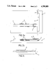
- FIG. 1 there is shown a simplified sketch of the top view and side view of one embodiment of the high-frequency excitation apparatus.
- FIG. 2 shows another embodiment of the high-frequency excitation apparatus in which provision is made for mounting the discharge tube in a manner that allows use of a flat ground plane.
- FIG. 3 shows a side view of the apparatus of FIG. 1 immersed in a non-conducting fluid.
- FIG. 1 The principal features of construction of the microwave system are shown in FIG. 1.
- a high-power high-frequency (200 MHz to 10 GHz) electrical wave is guided to the discharge region 1 by the transmission line formed by conductor 2 and ground plane 3.
- the characteristic impedance of this line is primarily determined by the width of the conductor and its separation from the ground plane, and the dielectric constant of the material 4 in the high-field region between the conductor and ground plane.
- Insertion of tuning slugs 5 constructed from materials with dielectric constant different from that of metal and/or dielectric material 4 between the conductor and ground plane perturbs the characteristic impedance of the transmission line and produces an impedance transforming effect as the electrical wave traverses the portion of the transmission line occupied by the tuning slugs.
- the two slugs together form an impedance transforming device known in the art of microwave engineering as a double slug tuner.
- the magnitude of the effective impedance of the microwave source at an arbitrary position 6 on the transmission line can be varied by adjusting the slug separation, S, and the phase of the effective source impedance at arbitrary position 6 can be adjsuted by changing the length, L. Consequently the effective impedance of the generator at point 6 can be adjusted to be the complex conjugate of the impedance presented by the discharge at 6 providing completely efficient transfer of power from the generating to the discharge.
- Uniform excitation of the discharge plasma along the length of the discharge tube 7 requires that the electric field in the region occupied by the discharge tube also be relatively uniform.
- the electric field at any point along the length of the electrode 8 is proportional to the voltage on the electrode 8 at that point and approximately inversely proportional to separation between the electrode 8 and the groud plane 3 at that point. If the length of the electrode 8 is greater than approximately 1/8 of the wavelength of the applied electric field, standing wave effects are likely to cause variation of the local electrode voltage along its length of the electrode. This voltage variation will result in nonuniform excitation of the plasma if the separation between the electrode 8 and ground plane 3 is constant.
- the electrode 8 by shaping the electrode 8 so that the separation between the electrode and ground plate 3 increases in regions where the local electrode voltage is high and decreases in regions where the electrode voltage is low, power deposition into the plasma can be maintained at a relatively uniform level along the portion of the discharge tube 7 lying between the electrode 8 and the ground plane 3.
- the voltage variation is first measured and then the electrode 8 is shaped to compensate for the variance due to the standing wave.
- the electrode distance to the tube 7 is therefore proportioned to the voltage.
- a high-voltage pulse to the discharge electrode prior to excitation by high-frequency fields effects preionization of the gas and assures effective delivery of the high-frequency electrical power to the discharge plasma.
- This pulse may be applied by means of a conductor bonded or otherwise attached to the electrode 8. Since the high-voltage preionization pulse can damage the high-frequency generator and associated circuitry, and the high-frequency circuitry can interfere with proper delivery of the high-voltage pulse to the electrode it is desirable to electrically isolate the high-frequency portion of the excitation system from the electrode by inserting a suitable capacitor between the electrode 8 and the transmission line conductor 2. An appropriate capacitor can be formed by placing a dielectric sheet 9 between electrode 8 and conductor 2. The dielectric material 9 should exhibit low loss at the excitation frequency utilized and sufficient dielectric strength and thickness to withstand the electric fields produced by the discharge control pulse.
- FIG. 2 shows a variation of the embodiment of FIG. 1, wherein the ground plane 3 is formed as a flat sheet and the electrode 8 extends above the discharge tube 7.
- the operation of the apparatus of FIG. 2 is the same as that of FIG. 1.
- FIG. 3 shows the apparatus of FIG. 1 immersed in a nonconducting fluid 10.
Landscapes
- Physics & Mathematics (AREA)
- Engineering & Computer Science (AREA)
- Plasma & Fusion (AREA)
- Chemical & Material Sciences (AREA)
- Analytical Chemistry (AREA)
- Electromagnetism (AREA)
- Optics & Photonics (AREA)
- Spectroscopy & Molecular Physics (AREA)
- Plasma Technology (AREA)
Abstract
Description
Claims (14)
Priority Applications (1)
| Application Number | Priority Date | Filing Date | Title |
|---|---|---|---|
| US07/028,111 US4789809A (en) | 1987-03-19 | 1987-03-19 | High frequency discharge apparatus with impedance matching |
Applications Claiming Priority (1)
| Application Number | Priority Date | Filing Date | Title |
|---|---|---|---|
| US07/028,111 US4789809A (en) | 1987-03-19 | 1987-03-19 | High frequency discharge apparatus with impedance matching |
Publications (1)
| Publication Number | Publication Date |
|---|---|
| US4789809A true US4789809A (en) | 1988-12-06 |
Family
ID=21841638
Family Applications (1)
| Application Number | Title | Priority Date | Filing Date |
|---|---|---|---|
| US07/028,111 Expired - Lifetime US4789809A (en) | 1987-03-19 | 1987-03-19 | High frequency discharge apparatus with impedance matching |
Country Status (1)
| Country | Link |
|---|---|
| US (1) | US4789809A (en) |
Cited By (7)
| Publication number | Priority date | Publication date | Assignee | Title |
|---|---|---|---|---|
| WO1990014749A1 (en) * | 1989-05-19 | 1990-11-29 | The University Of British Columbia | Furnace atomization atmospheric pressure capacitively coupled plasma excitation source |
| US4990829A (en) * | 1989-04-21 | 1991-02-05 | Potomac Photonics, Inc. | High frequency discharge apparatus with hollow waveguide input section |
| FR2826542A1 (en) * | 2001-06-22 | 2002-12-27 | Pantechnik | DEVICE FOR THE PRODUCTION OF VARIABLE POSITIVE LOADS WITH CYCLOTRON RESONANCE |
| US6518703B1 (en) * | 1998-03-16 | 2003-02-11 | Matsushita Electrical Industrial Co., Ltd. | Electrodeless discharge energy supply apparatus and electrodeless discharge lamp device using surface wave transmission line |
| US6747299B2 (en) * | 2001-03-30 | 2004-06-08 | Fujitsu Quantum Devices Limited | High frequency semiconductor device |
| US20110025139A1 (en) * | 2009-08-03 | 2011-02-03 | Schulte David J | Power generator |
| US20110127776A1 (en) * | 2009-08-03 | 2011-06-02 | Schulte David J | Power generator |
Citations (5)
| Publication number | Priority date | Publication date | Assignee | Title |
|---|---|---|---|---|
| US2760163A (en) * | 1954-10-11 | 1956-08-21 | Itt | Radio frequency propagating systems |
| US2798186A (en) * | 1955-04-19 | 1957-07-02 | Bomac Lab Inc | Electron discharge device for microstrip transmission systems |
| US3621463A (en) * | 1970-04-27 | 1971-11-16 | Bell Telephone Labor Inc | Negative resistance diode coaxial oscillator with resistive spurious frequency suppressor |
| US4472690A (en) * | 1982-06-14 | 1984-09-18 | Rockwell International Corporation | Universal transistor characteristic matching apparatus |
| US4631732A (en) * | 1984-04-25 | 1986-12-23 | Christensen Clad P | High frequency RF discharge laser |
-
1987
- 1987-03-19 US US07/028,111 patent/US4789809A/en not_active Expired - Lifetime
Patent Citations (5)
| Publication number | Priority date | Publication date | Assignee | Title |
|---|---|---|---|---|
| US2760163A (en) * | 1954-10-11 | 1956-08-21 | Itt | Radio frequency propagating systems |
| US2798186A (en) * | 1955-04-19 | 1957-07-02 | Bomac Lab Inc | Electron discharge device for microstrip transmission systems |
| US3621463A (en) * | 1970-04-27 | 1971-11-16 | Bell Telephone Labor Inc | Negative resistance diode coaxial oscillator with resistive spurious frequency suppressor |
| US4472690A (en) * | 1982-06-14 | 1984-09-18 | Rockwell International Corporation | Universal transistor characteristic matching apparatus |
| US4631732A (en) * | 1984-04-25 | 1986-12-23 | Christensen Clad P | High frequency RF discharge laser |
Cited By (10)
| Publication number | Priority date | Publication date | Assignee | Title |
|---|---|---|---|---|
| US4990829A (en) * | 1989-04-21 | 1991-02-05 | Potomac Photonics, Inc. | High frequency discharge apparatus with hollow waveguide input section |
| WO1990014749A1 (en) * | 1989-05-19 | 1990-11-29 | The University Of British Columbia | Furnace atomization atmospheric pressure capacitively coupled plasma excitation source |
| US6518703B1 (en) * | 1998-03-16 | 2003-02-11 | Matsushita Electrical Industrial Co., Ltd. | Electrodeless discharge energy supply apparatus and electrodeless discharge lamp device using surface wave transmission line |
| US6747299B2 (en) * | 2001-03-30 | 2004-06-08 | Fujitsu Quantum Devices Limited | High frequency semiconductor device |
| FR2826542A1 (en) * | 2001-06-22 | 2002-12-27 | Pantechnik | DEVICE FOR THE PRODUCTION OF VARIABLE POSITIVE LOADS WITH CYCLOTRON RESONANCE |
| EP1272015A1 (en) * | 2001-06-22 | 2003-01-02 | Pantechnik | Cyclotron resonance device for the generation of ions with variable positive charge |
| US20110025139A1 (en) * | 2009-08-03 | 2011-02-03 | Schulte David J | Power generator |
| US20110127776A1 (en) * | 2009-08-03 | 2011-06-02 | Schulte David J | Power generator |
| US8203224B2 (en) * | 2009-08-03 | 2012-06-19 | Schulte David J | Power generator |
| US8508057B2 (en) * | 2009-08-03 | 2013-08-13 | David J. Schulte | Power generator |
Similar Documents
| Publication | Publication Date | Title |
|---|---|---|
| JPH09293600A (en) | High frequency power application device, plasma generation device, plasma processing device, high frequency power application method, plasma generation method and plasma processing method | |
| JPH0130319B2 (en) | ||
| US2323201A (en) | Tuned circuit and associated devices therefor | |
| US4789809A (en) | High frequency discharge apparatus with impedance matching | |
| US2557180A (en) | Apparatus for coupling ultra high frequency systems | |
| US3212034A (en) | Electromagnetic wave energy filtering | |
| US3443244A (en) | Coaxial resonator structure for solid-state negative resistance devices | |
| US3546624A (en) | Electronically tuned solid state oscillator | |
| US3909746A (en) | YIG-tuned push-pull microwave diode oscillator | |
| US3601723A (en) | Electronic tuning apparatus for microwave circuits | |
| US4083016A (en) | Coupled-cavity microwave oscillator | |
| US3659222A (en) | High efficiency mode avalanche diode oscillator | |
| Lee et al. | Bandwidth enhancement of dielectric resonator antennas | |
| US4342009A (en) | Electronically tuned Gunn oscillator and mixer including the same | |
| US4990829A (en) | High frequency discharge apparatus with hollow waveguide input section | |
| US4656438A (en) | Power combining cavity | |
| US2951207A (en) | Parametric amplifier | |
| US3659223A (en) | Microwave oscillator with two or more paralleled semiconductive devices | |
| US3416099A (en) | Bulk-effect negative-resistance microwave device employing a half wave open circuit resonator structure | |
| US3969689A (en) | Dual diode oscillator and airstrip transmission line apparatus | |
| US3842370A (en) | Coaxial trapatt oscillator operable at a fixed frequency and at a high efficiency | |
| JPH08316212A (en) | Plasma processing method and plasma processing apparatus | |
| US2725531A (en) | Gas discharge coupling device for waveguides | |
| US3731180A (en) | Frequency translator circuit | |
| US3842359A (en) | Balanced parametric amplifier |
Legal Events
| Date | Code | Title | Description |
|---|---|---|---|
| AS | Assignment |
Owner name: POTOMAC PHOTONICS, INC., ENGINEERING RRESEARCH CEN Free format text: ASSIGNMENT OF ASSIGNORS INTEREST.;ASSIGNOR:CHRISTENSEN, C. PAUL;REEL/FRAME:004913/0417 Effective date: 19880516 Owner name: POTOMAC PHOTONICS, INC.,MARYLAND Free format text: ASSIGNMENT OF ASSIGNORS INTEREST;ASSIGNOR:CHRISTENSEN, C. PAUL;REEL/FRAME:004913/0417 Effective date: 19880516 |
|
| STCF | Information on status: patent grant |
Free format text: PATENTED CASE |
|
| FPAY | Fee payment |
Year of fee payment: 4 |
|
| FEPP | Fee payment procedure |
Free format text: PAYOR NUMBER ASSIGNED (ORIGINAL EVENT CODE: ASPN); ENTITY STATUS OF PATENT OWNER: SMALL ENTITY |
|
| FPAY | Fee payment |
Year of fee payment: 8 |
|
| REMI | Maintenance fee reminder mailed | ||
| FPAY | Fee payment |
Year of fee payment: 12 |
|
| SULP | Surcharge for late payment |