US4788593A - High resolution scanning system including optical enlargement - Google Patents
High resolution scanning system including optical enlargement Download PDFInfo
- Publication number
- US4788593A US4788593A US06/918,953 US91895386A US4788593A US 4788593 A US4788593 A US 4788593A US 91895386 A US91895386 A US 91895386A US 4788593 A US4788593 A US 4788593A
- Authority
- US
- United States
- Prior art keywords
- thin film
- pattern
- photosensor array
- information
- array
- Prior art date
- Legal status (The legal status is an assumption and is not a legal conclusion. Google has not performed a legal analysis and makes no representation as to the accuracy of the status listed.)
- Expired - Lifetime
Links
Images

Classifications
-
- H—ELECTRICITY
- H04—ELECTRIC COMMUNICATION TECHNIQUE
- H04N—PICTORIAL COMMUNICATION, e.g. TELEVISION
- H04N1/00—Scanning, transmission or reproduction of documents or the like, e.g. facsimile transmission; Details thereof
- H04N1/04—Scanning arrangements, i.e. arrangements for the displacement of active reading or reproducing elements relative to the original or reproducing medium, or vice versa
- H04N1/19—Scanning arrangements, i.e. arrangements for the displacement of active reading or reproducing elements relative to the original or reproducing medium, or vice versa using multi-element arrays
- H04N1/195—Scanning arrangements, i.e. arrangements for the displacement of active reading or reproducing elements relative to the original or reproducing medium, or vice versa using multi-element arrays the array comprising a two-dimensional [2D] array
Definitions
- This invention relates generally to image scanning systems and, more particularly, to electronic imaging systems which include therein a thin film photosensor array and which are adapted to detect a pattern of information and provide an output signal corresponding thereto.
- image or optical scanners are defined as systems including one or more photosensor arrays operatively disposed to scan a pattern of information or data and generate electrical signals corresponding thereto.
- Optical scanners may be readily adapted to address a wide variety of data inputs.
- the data may be a pattern of graphic information in the form of a photograph, a drawing, a design on fabric or the like, or the information being scanned may be alpha-numeric data such as printed or written matter. In other instances, the information may be a three dimensional pattern, such as the surface of a solid.
- optical scanners convert a pattern of data into electrical signals which may be supplied to downstream apparatus for further processing, storage or display.
- Image scanners are incorporated into facsimile machines, copying machines, computer input terminals, CAD-CAM systems and the like. Additionally, image scanners are utilized in production processes to inspect surfaces of materials such as plywood, fabric, plastic's textile, and metal.
- the typical image scanner includes one or more photoresponsive circuits configured and disposed so as to either simultaneously or sequentially address various portions of the surface being scanned.
- CCDs Charge coupled devices
- CCDs are solid state devices, typically formed from single crystal silicon and include therein an array of photosensor elements.
- CCDs have a high degree of photosensitivity and are capable of providing high resolution.
- CCDs are relatively small in size; the typical CCD array is a two dimensional matrix approximately one centimeter square, and the largest CCDs currently produced are one dimensional arrays no greater than approximately 3 to 4 inches in length.
- These size contraints impose restrictions on the utility of CCDs in scanners.
- an optical system must be utilized to project that pattern of information at a reduced size onto the surface of the CCD. Such optical systems will effectively reduce the resolution of the CCD.
- a typical two dimensional CCD array is one centimeter square and includes therein 256,000 photosensor units, generally referred to as pixels.
- the equivalent resolution would be about 50 lines/mm for the one centimeter square CCD array. If a pattern of information occupying an area of 35 ⁇ 35 millimeters were projected down onto this one centimeter square charge coupled device, the effective resolution of the 35 millimeter square image would fall to approximately 15 lines/mm.
- medium resolution photographic film is generally capable of resolving approximately 120 lines/mm.
- Efforts to improve resolution using single crystal integrated circuits encounter at least two significant problems.
- the first is that integrated circuit chips formed on single crystal silicon wafers must be as small as possible to enable acceptable yields and to meet requirements of economical manufacturing.
- the second problem, related to the first, is that in order to increase the packing density in the small available chip area, finer and finer photolithography must be used with resulting increases in the cost of manufacture. For these reasons, among others, high resolution sensing (high resolution being defined relative to photographic capabilities) of patterns of information of practical size with present CCD technology is not economically achievable.
- one centimeter square CCDs may ultimately be fabricated to include 1.4 million pixels therein. This translates to a resolution of approximately 120 lines/mm on the one centimeter square device and a corresponding effective resolution of 34 lines/mm for a 35 millimeter square pattern of information projected thereonto.
- the only way the resolution of the CCD could be further increased is by increasing either the density of pixels in the CCD or the size of the device itself. Both approaches present significant problems.
- the difraction limit of light will ultimately impose limits on any photolithographic process utilized to pattern CCDs although constraints of practicality and cost will generally intervene first to set the limit on pixel density.
- processing constraints will limit the size of crystalline CCDs that can be manufactured.
- Single crystal wafers cannot generally be economically manufactured in sizes exceeding perhaps six to eight inches in diameter. Furthermore, processing steps can introduce defects into such devices. Increasing the size of a crystalline device, especially while maintaining strict limits on the size of the photolithographic features thereof imposes a great burden of cost insofar as the likelihood of creating defects exponentially increases along with a dramatic decrease in the yield of devices. The result is that the cost of finished product increases exponentially with increasing device size. It will thus be appreciated that even utilizing the most optimistically projected pixel densities and single crystalline CCD sizes, high resolution optical scanners adapted to sense a pattern of information in an area exceeding several square inches cannot be economically manufactured utilizing such technology.
- Deposited thin film devices represent another approach to the fabrication of optical scanners.
- Thin film devices may be economically manufactured over large areas by the vapor deposition of layers of appropriate semiconductor materials onto a variety of substrates. By appropriately patterning these layers, for example, through the use of presently available photolithographic techniques, a variety of device configurations may be provided.
- amorphous materials include all materials or alloys which have long range disorder although they may have short or intermediate range order, or even contain at times, crystalline inclusions.
- microcrystalline is defined as a unique class of said amorphous materials characterized by a volume fraction of crystalline inclusions, said volume fraction of inclusions being greater than a threshold value at which the onset of substantial changes in certain key parameters such as electrical conductivity, band gap and absorption constant occur.
- Thin film semiconductor alloys may be readily manufactured to cover large areas by mass production processes and therefore provide for the economic fabrication of large scale image sensor arrays.
- the use of such large arrays eliminates the need for optically reducing a pattern of information so as to conform that pattern to a small area sensor array, thereby eliminating the loss of resolution described above for CCD arrays.
- the thin film sensor arrays can be fabricated to be larger than the pattern of information being scanned, that pattern can be optically projected onto the array in an enlarged form thereby increasing the effective resolution of the array. In this manner, high resolution image reproduction may be achieved without the need for employing precision photolithographic techniques, thereby maintaining high product yields and low manufacturing costs.
- a thin film photosensor array is fabricated having a 50 micron pitch, that is to say 50 microns center-to-center spacing between the adjacent photosensitive elements thereof, the array will provide a resolution of 20 lines/mm. This resolution is better than that attainable when scanning a 35 millimeter square pattern of information with presently available CCDs. A fifty micron pitch is readily achieved at very high yields utilizing conventional photolithographic techniques. If the pitch remained the same and a photosensor array of approximately 54 millimeters on an edge were fabricated, a 1.4 million pixel array would be realized. Thus, it may be seen that by increasing the size of the photosensor array, and with presently available processing techniques, resolution equivalent to the best anticipated resolution for single crystal charge coupled devices is presently equaled. Since thin film photosensor arrays can be made in sizes up to several feet, even assuming no new advances in said technology, the resolving power of charge coupled devices can be exceeded by orders of magnitude with such thin film arrays.
- Sensing a pattern of information may be accomplished with a linear array of photosensitive elements by scanning, or passing that array across the pattern of information. It is presently possible to fabricate linear photosensor arrays in sizes exceeding several meters. The use of such arrays in conjunction with the projection of an enlarged image there provides for ultra-high resolution photosensing of informational patterns. Techniques for the fabrication of such large arrays are found in U.S. patent application Ser. No. 885,907, now U.S. Pat. No.
- the instant invention eliminates constraints heretofore present in optical scanning systems utilizing charge coupled or similar integrated circuits fabricated on single crystal wafers devices as photosensors.
- the present invention thus makes possible high resolution optical scanning systems which are easy to fabricate, low in cost and adaptable for the scanning of graphic and/or alpha-numeric data.
- the method includes the steps of providing a thin film photosensor array, providing optical means adapted to generate an enlarged image of a pattern of information, projecting said enlarged image for sensing by said photosensor array and sensing the enlarged image with the thin film photosensor array so as to provide a signal corresponding thereto.
- the apparatus includes optical means adapted to generate an enlarged image of the pattern of information and a thin film photosensor array disposed so as to sense the enlarged image and provide a signal corresponding thereto.
- the thin film photosensor array includes at least one layer of semiconductor material chosen from the group consisting essentially of: amorphous silicon alloy materials, amorphous germanium alloy materials, and amorphous silicon germanium alloy materials.
- the optical means may include a lens or a mirror. In some instances the optical means is adapted to project the enlarged image directly onto the thin film photosensor array whereas in other instances it is adapted to project the image onto a screen and the thin film photosensor array is disposed so as to sense the image projected on the screen.
- the pattern of information may be a transparency which is projected by the optical means to form an enlarged image thereof.
- the pattern of information may be a three dimensional body and the optical means may be adapted to generate an enlarged two dimensional image of at least a portion of the surface of the three dimensional body.
- the thin film photosensor array may comprise a planar array or may be a flexible array contoured to generally correspond to the focal plane of the optical means.
- the thin film photosensor array may be a linear array of photosensitive elements, in which case the apparatus will further include means for scanning the enlarged image with the linear array.
- the thin film photosensor array is a two dimensional array.
- the photosensor array may include photoresponsive elements selected from the group consisting essentially of photodiodes, phototransistors, photoconductive devices, photovoltaic devices, and combinations thereof.
- the photoresponsive devices of the array may include two oppositely doped layers of semiconductor material and in yet other instances, may also include a layer of substantially intrinsic semiconductor material interposed therebetween.
- the apparatus may be adapted to provide a digital signal or an analog signal corresponding to the pattern of information being sensed and may further include a display device or a printer.
- One specific embodiment of the instant invention includes a method and apparatus for providing an electronic signal indicative of the pattern of information in a fingerprint.
- This apparatus includes optical means adapted to project an enlarged image of the fingerprint and a thin film photosensor array disposed so as to sense the enlarged image and provide a corresponding output signal.
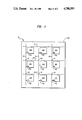
- FIG. 1 is a top plan view of one particular type of thin film photosensor array which may be utilized in the practice of the instant invention
- FIG. 2 is a schematic illustration of a prior art optical scanning system utilizing a single crystalline charge coupled device
- FIG. 3 is a schematic illustration of an optical scanning system of the present invention as adapted to utilize a two dimensional, thin film photosensor array
- FIG. 4 is a schematic illustration of an optical scanning system of the instant invention as adapted to utilize a linear, thin film photosensor array.
- FIG. 1 there is shown in top plan view one particular thin film photosensor array 10, typical of those which may be utilized in the practice of the present invention, it being kept in mind that other photosensor arrays may be similarly employed.
- the photosensor array 10 is comprised of a plurality of photosensitive elements 12a-12i arrayed in a two-dimensional matrix form. Each of the photosensitive elements, 12a-12i, has associated therewith an isolation device 14a-14i interconnecting that element 12 to a grid of address lines. As illustrated the grid includes a plurality of X address lines 16, 18 and 20 and a plurality of Y address lines 22, 24 and 26, formed of an electrically conductive material such as a metal or the like.
- the photosensor array 10 is formed upon a substrate 28, which may be a rigid member substrate such as a glass, or metallic plate, or a flexible member such as a thin metallic member, or a sheet of synthetic polymeric material. In those instances where the substrate 28 is electrically conductive, it may be desirable to provide an insulating coating thereatop prior to the deposition of the address lines thereon.
- the photosensor elements 12a-12i are photoresponsive elements, that is to say they are adapted to produce a detectable signal in response to the absorption of illumination. This signal may comprise a current, a voltage, a change in resistivity or the like.
- devices which may be utilized as photosensors 12 are photodiodes, phototransistors, photoconductive devices, photovoltaic devices and the like taken either singly or in combination.
- One group of photosensor devices having particular utility are p-i-n photovoltaic devices comprised of two oppositely doped layers of semiconductor material having a body of substantially intrinsic semiconductor material therebetween. Such devices may be used either singly or in stacked tandem combinations to produce voltage and/or current in response to the absorption of illumination.
- the isolation device 14, associated with each of the photosensor elements is utilized to restrict the flow of electrical current through the photosensor array 10 to predetermined paths so as to facilitate addressing of particular photosensor elements 12.
- the isolation device 14 may comprise any type of control device such as a diode, a transistor, a threshold switch, a relay or the like. P-I-N type diodes have been found to be particularly useful in the fabrication of photosensor arrays.
- the address lines 16, 18, 20, 22, 24 and 26 are arrayed in a X-Y matrix and electrically isolated at cross-over points 19. By addressing particular pairs of address lines, distinct photosensors may be accessed. For example, by addressing line 24 and line 18 sensor 12e is accessed. The presence of the blocking devices 14 on adjoining elements prevents the communication of unwanted electrical signals during addressing.
- amorphous silicon alloy materials refers to those alloys of silicon with other elements or materials as for example, compensating or modifying elements such as hydrogen, halogens, carbon and/or nitrogen.
- germanium alloy materials shall refer to germanium in combination with other elements or materials.
- amorphous silicon germanium alloy shall include all alloys which include both silicon and germanium in any proportion with or without other elements or materials.
- photosensor array 10 of FIG. 1 is depicted as being a two dimensional matrix comprised of nine photosensor elements, in practicality an array comprised of a much larger number of elements will generally be preferred. It will also be apparent that while the array 10 of FIG. 1 is depicted as being a two dimensional array similar technology may be readily modified to provide a one dimensional, i.e. linear, array. Detailed descriptions of the operations and fabrication of both one and two dimensional sensor arrays will be found in the patents referred to and incorporated by reference hereinabove.
- FIG. 2 there is illustrated in schematic form an apparatus as adapted for sensing of a pattern of information with a charge coupled device. As such, FIG. 2 represents the state of the prior art.
- a charge coupled device such as a two dimensional, single crystalline charge coupled device 30 is disposed so as to sense a pattern of information embodied in an object 32, shown here as an arrow. Since the object 32 is larger than the active area of the charge coupled device 30, an optical system, represented here schematically as a lens 34 is utilized to project a reduced size image 36 of the object 32 onto the charge coupled device 30.
- an optical system represented here schematically as a lens 34 is utilized to project a reduced size image 36 of the object 32 onto the charge coupled device 30.
- the charge coupled device 30 is 1 centimeter square and includes 256,000 pixels, it will have a resolving power of approximately 50 lines per millimeter. If the object 32 being sensed is 3.5 centimeters long and is projected in a reduced form to provide an image 36 which fills the active area of the charge coupled device 30; that object 32, will be imaged with an effective resoultion of approximately 15 lines per millimeter.
- FIG. 3 there is shown also in schematic form one embodiment of the instant invention as adapted to provide for the high resolution sensing of a pattern of information.
- the illustrated embodiment depicts an object 32 and an optical system shown as a lens 34, as disposed to project an image 38 of the object 32 onto a thin film photosensor array 40.
- the projected image 38 is considerably larger than the original object 32.
- the photosensor array 40 is a thin film photosensor array generally similar to those described with reference to FIG. 1.
- effective resolution of the array is increased.
- photosensor arrays may be readily fabricated in high yield having a pitch of approximately 50 microns, that is to say a center-to-center spacing of 50 microns between adjacent photosensor elements. This provides a resolution of 20 line pairs per millimeter, a number exceeding the effective resolution of the charge coupled device in the FIG. 2 embodiment. If the image 38 of the object 32 being sensed is being projected onto the array 40 at a twofold magnification this resolution will effectively be doubled. Still higher magnifications will produce correspondingly greater effective resolution values.
- the photosensor array 40 has downstream signal processing equipment 42 associated therewith.
- downstream processing equipment may include a computer for enhancing, manipulating or otherwise processing images produced by the sensor array.
- the downstream processing apparatus may also include a video display terminal or printing apparatus for producing an image of the object being sensed; likewise, downstream processing may include storage apparatus such as a magnetic disk or an optical disk.
- FIG. 4 illustrates still another embodiment of the present invention utilizing a linear array of photosensors 44 to scan a projected image 38 of an object 32.
- the apparatus of the FIG. 4 embodiment may include drive means to advance the linear photosensor array 44 across the plane of the image 38, as indicated by broken arrows A, A'.
- the optical system 34 may be adapted to sweep the projected image 38 across the linear array 44.
- the optical system although indicated by a lens 34 in the Figures, may alternatively include a mirror or other such optical element for providing the enlarged image.
- the object being imaged may comprise a three dimensional solid body, which has a two dimensional representation thereof projected onto the photosensor array, but in other instances the object being imaged may be a planar member, such as a photograph, a page of text or a pattern upon a sheet of material, which is projected onto the sensor array.
- the object bearing the pattern of information being scanned may comprise a transparency which is projected onto the sensor array by an optical system akin to that of a slide projector. In some instances, it may be more expedient to project the image of the object onto a translucent screen, and to then scan the screen with the photosensor array.
- the present invention will have utility in many imaging applications, such as systems for the scanning, transmitting and processing of data.
- One such embodiment is as a fingerprint scanning device adapted to sense the pattern of information present in a fingerprint and provide an electrical signal indicative thereof.
- Fingerprint patterns may be readily provided on transparent or semi-transparent media such as paper, plastic films, glass and the like by conventionally applying ink to the surface of a finger and contacting it to the medium; an image sensing system structured in accord with the present invention may then be utilized to scan the fingerprint image.
- High resolution transparency images of fingerprints, or other such topological features of tissue may be instantaneously recorded in a photodispersion film by the application of a brief light and/or heat pulse thereto.
- the method and apparatus for practice of such invention are disclosed in U.S. Pat. No. 4,251,564 entitled "Heat Sink Imaging Method And Apparatus For Live Skin Tissue Using Pulsed Energy Source," the disclosure of which is disclosed herein by reference.
- a high resolution enlarged image of the fingerprint pattern may be readily projected onto a photosensor array for the generation of an electrical signal corresponding thereto.
- the information on the fingerprint may be analyzed and encoded through a cross reference scheme for later analysis, retrieval, or transmission to remote locations for storage or display.
- Thin film photosensor arrays may be readily fabricated in large areas upon flexible substrates making them adaptable for a wide variety of imaging applications.
- the sensor array need not be planar as shown in the Figures, but may curved so as to accomodate the optical system being employed. For example, if an optical system has a degree of abberation producing a curved plane of focus, a flexible array of photosensors may be disposed so as to correspond to this curved image plane.
- Thin film photosensor arrays may be readily fabricated in very large areas and accordingly may be utilized with optical systems giving high magnification ratios to produce ultra-high resolution image scans.
- resolution of an imaging array is enhanced by the use of optical enlargement of a data pattern prior to sensing thereof.
- Such an arrangement allows for very high resolution scanning and permits the use of relatively coarse featured photolithography in the preparation of the sensor arrays.
Landscapes
- Engineering & Computer Science (AREA)
- Multimedia (AREA)
- Signal Processing (AREA)
- Facsimile Heads (AREA)
- Solid State Image Pick-Up Elements (AREA)
- Facsimile Scanning Arrangements (AREA)
- Transforming Light Signals Into Electric Signals (AREA)
Abstract
Description
Claims (19)
Priority Applications (4)
| Application Number | Priority Date | Filing Date | Title |
|---|---|---|---|
| US06/918,953 US4788593A (en) | 1986-10-15 | 1986-10-15 | High resolution scanning system including optical enlargement |
| CA000545886A CA1278078C (en) | 1986-10-15 | 1987-09-01 | High resolution optical scanning system and method |
| EP87308140A EP0265067A3 (en) | 1986-10-15 | 1987-09-15 | High resolution optical scanning and method |
| JP62260739A JPS63108772A (en) | 1986-10-15 | 1987-10-15 | Method and apparatus for high resolution optical scanning |
Applications Claiming Priority (1)
| Application Number | Priority Date | Filing Date | Title |
|---|---|---|---|
| US06/918,953 US4788593A (en) | 1986-10-15 | 1986-10-15 | High resolution scanning system including optical enlargement |
Publications (1)
| Publication Number | Publication Date |
|---|---|
| US4788593A true US4788593A (en) | 1988-11-29 |
Family
ID=25441221
Family Applications (1)
| Application Number | Title | Priority Date | Filing Date |
|---|---|---|---|
| US06/918,953 Expired - Lifetime US4788593A (en) | 1986-10-15 | 1986-10-15 | High resolution scanning system including optical enlargement |
Country Status (4)
| Country | Link |
|---|---|
| US (1) | US4788593A (en) |
| EP (1) | EP0265067A3 (en) |
| JP (1) | JPS63108772A (en) |
| CA (1) | CA1278078C (en) |
Cited By (4)
| Publication number | Priority date | Publication date | Assignee | Title |
|---|---|---|---|---|
| US5274456A (en) * | 1987-12-28 | 1993-12-28 | Hitachi, Ltd. | Semiconductor device and video camera unit using it and their manufacturing method |
| US6573507B1 (en) * | 1998-12-24 | 2003-06-03 | Fuji Photo Film Co., Ltd. | Radiation image read-out method and apparatus with transformed pixel density based on radiation image size |
| US8360973B2 (en) * | 2000-11-29 | 2013-01-29 | L'oreal | Process for acquiring scanned image data relating to an external body portion and/or a product applied thereto |
| US10366493B2 (en) | 2016-05-27 | 2019-07-30 | Samsung Display Co., Ltd. | Display device and method of fabricating the same |
Families Citing this family (1)
| Publication number | Priority date | Publication date | Assignee | Title |
|---|---|---|---|---|
| US4845552A (en) * | 1987-08-20 | 1989-07-04 | Bruno Jaggi | Quantitative light microscope using a solid state detector in the primary image plane |
Citations (2)
| Publication number | Priority date | Publication date | Assignee | Title |
|---|---|---|---|---|
| US4607168A (en) * | 1982-07-09 | 1986-08-19 | Hitachi, Ltd. | Photosensor array devices |
| US4660095A (en) * | 1984-05-04 | 1987-04-21 | Energy Conversion Devices, Inc. | Contact-type document scanner and method |
Family Cites Families (6)
| Publication number | Priority date | Publication date | Assignee | Title |
|---|---|---|---|---|
| EP0053946B1 (en) * | 1980-12-10 | 1988-06-01 | Fuji Xerox Co., Ltd. | Elongate thin-film reader |
| JPS59226557A (en) * | 1983-06-07 | 1984-12-19 | Sharp Corp | Two-dimensional picture reading device |
| SE446801B (en) * | 1983-09-20 | 1986-10-06 | Hasselblad Ab Victor | DEVICE FOR MANUFACTURING ELECTRONIC, DIGITAL IMAGE INFORMATION |
| JPS60161664A (en) * | 1984-02-01 | 1985-08-23 | Sharp Corp | Tightly adhered two-dimensional image readout device |
| EP0163956A3 (en) * | 1984-05-04 | 1988-04-06 | Energy Conversion Devices, Inc. | Intergrated radiation sensing array |
| JPS61124168A (en) * | 1984-11-20 | 1986-06-11 | Matsushita Electric Ind Co Ltd | Close-contact image sensor |
-
1986
- 1986-10-15 US US06/918,953 patent/US4788593A/en not_active Expired - Lifetime
-
1987
- 1987-09-01 CA CA000545886A patent/CA1278078C/en not_active Expired - Fee Related
- 1987-09-15 EP EP87308140A patent/EP0265067A3/en not_active Withdrawn
- 1987-10-15 JP JP62260739A patent/JPS63108772A/en active Pending
Patent Citations (2)
| Publication number | Priority date | Publication date | Assignee | Title |
|---|---|---|---|---|
| US4607168A (en) * | 1982-07-09 | 1986-08-19 | Hitachi, Ltd. | Photosensor array devices |
| US4660095A (en) * | 1984-05-04 | 1987-04-21 | Energy Conversion Devices, Inc. | Contact-type document scanner and method |
Cited By (4)
| Publication number | Priority date | Publication date | Assignee | Title |
|---|---|---|---|---|
| US5274456A (en) * | 1987-12-28 | 1993-12-28 | Hitachi, Ltd. | Semiconductor device and video camera unit using it and their manufacturing method |
| US6573507B1 (en) * | 1998-12-24 | 2003-06-03 | Fuji Photo Film Co., Ltd. | Radiation image read-out method and apparatus with transformed pixel density based on radiation image size |
| US8360973B2 (en) * | 2000-11-29 | 2013-01-29 | L'oreal | Process for acquiring scanned image data relating to an external body portion and/or a product applied thereto |
| US10366493B2 (en) | 2016-05-27 | 2019-07-30 | Samsung Display Co., Ltd. | Display device and method of fabricating the same |
Also Published As
| Publication number | Publication date |
|---|---|
| EP0265067A3 (en) | 1989-07-19 |
| EP0265067A2 (en) | 1988-04-27 |
| CA1278078C (en) | 1990-12-18 |
| JPS63108772A (en) | 1988-05-13 |
Similar Documents
| Publication | Publication Date | Title |
|---|---|---|
| CA1292313C (en) | Electronic camera | |
| US4853785A (en) | Electronic camera including electronic signal storage cartridge | |
| US4644406A (en) | Large scale contact type image reading unit using two-dimensional sensor array | |
| US4587621A (en) | Device for electrical variable magnification of document image | |
| US4479149A (en) | Photo-electric converter and image forming apparatus incorporating the same | |
| US4768096A (en) | Contact-type portable digitizing wand for scanning image-bearing surfaces | |
| US4764682A (en) | Photosensitive pixel sized and shaped to optimize packing density and eliminate optical cross-talk | |
| US4788593A (en) | High resolution scanning system including optical enlargement | |
| GB2150785A (en) | Two-dimensional image read-out device | |
| JPS6366117B2 (en) | ||
| US4714836A (en) | Photosensitive pixel with exposed blocking element | |
| EP0119742B1 (en) | Two-dimensional image readout device | |
| US4659920A (en) | Image sensor arrays with series redundancy | |
| JPH0783098B2 (en) | Optical image detector manufacturing method and two-dimensional matrix detector manufactured by the manufacturing method | |
| US4746804A (en) | Photosensitive pixel with exposed blocking element | |
| EP3461114B1 (en) | Contact image sensor and image scanning device | |
| JPH0590557A (en) | Photoelectric converter and data processor | |
| Mimura et al. | A two-dimensional image sensor with aSi: H pin diodes | |
| JPS6276357A (en) | Solid-state image pickup device | |
| JPH022301B2 (en) | ||
| US4907088A (en) | Contact-type imager for use as the front end of copier apparatus | |
| JPS59161176A (en) | Two-dimensional picture reader | |
| US5734178A (en) | Imaging system using area sensor | |
| JPH01184951A (en) | Image scanner | |
| JPS6222299B2 (en) |
Legal Events
| Date | Code | Title | Description |
|---|---|---|---|
| AS | Assignment |
Owner name: ENERGY CONVERSION DEVICES, INC., 1675 W. MAPLE ROA Free format text: ASSIGNMENT OF ASSIGNORS INTEREST.;ASSIGNORS:OVSHINSKY, STANFORD R.;NORRIS, LAWRENCE G.;REEL/FRAME:004617/0727 Effective date: 19861010 |
|
| AS | Assignment |
Owner name: NATIONAL BANK OF DETROIT, 611 WOODWARD AVE., DETRO Free format text: SECURITY INTEREST;ASSIGNOR:ENERGY CONVERSION DEVICES, INC., A DE CORP;REEL/FRAME:004702/0031 Effective date: 19870324 Owner name: NATIONAL BANK OF DETROIT, A NATIONAL BANKING ASSO Free format text: SECURITY INTEREST;ASSIGNOR:ENERGY CONVERSION DEVICES, INC., A DE CORP;REEL/FRAME:004702/0031 Effective date: 19870324 |
|
| FEPP | Fee payment procedure |
Free format text: PAYOR NUMBER ASSIGNED (ORIGINAL EVENT CODE: ASPN); ENTITY STATUS OF PATENT OWNER: LARGE ENTITY |
|
| STCF | Information on status: patent grant |
Free format text: PATENTED CASE |
|
| AS | Assignment |
Owner name: ENERGY CONVERSION DEVICES, INC., MICHIGAN Free format text: RELEASED BY SECURED PARTY;ASSIGNOR:NATIONAL BANK OF DETROIT;REEL/FRAME:005300/0328 Effective date: 19861030 |
|
| REMI | Maintenance fee reminder mailed | ||
| FPAY | Fee payment |
Year of fee payment: 4 |
|
| SULP | Surcharge for late payment | ||
| FEPP | Fee payment procedure |
Free format text: PAYER NUMBER DE-ASSIGNED (ORIGINAL EVENT CODE: RMPN); ENTITY STATUS OF PATENT OWNER: LARGE ENTITY |
|
| FPAY | Fee payment |
Year of fee payment: 8 |
|
| FPAY | Fee payment |
Year of fee payment: 12 |