US4697248A - Arithmetic circuit for obtaining the vector product of two vectors - Google Patents
Arithmetic circuit for obtaining the vector product of two vectors Download PDFInfo
- Publication number
- US4697248A US4697248A US06/685,125 US68512584A US4697248A US 4697248 A US4697248 A US 4697248A US 68512584 A US68512584 A US 68512584A US 4697248 A US4697248 A US 4697248A
- Authority
- US
- United States
- Prior art keywords
- gates
- output
- arithmetic circuit
- sup
- supplied
- Prior art date
- Legal status (The legal status is an assumption and is not a legal conclusion. Google has not performed a legal analysis and makes no representation as to the accuracy of the status listed.)
- Expired - Lifetime
Links
Images


Classifications
-
- G—PHYSICS
- G06—COMPUTING OR CALCULATING; COUNTING
- G06F—ELECTRIC DIGITAL DATA PROCESSING
- G06F7/00—Methods or arrangements for processing data by operating upon the order or content of the data handled
- G06F7/60—Methods or arrangements for performing computations using a digital non-denominational number representation, i.e. number representation without radix; Computing devices using combinations of denominational and non-denominational quantity representations, e.g. using difunction pulse trains, STEELE computers, phase computers
- G06F7/72—Methods or arrangements for performing computations using a digital non-denominational number representation, i.e. number representation without radix; Computing devices using combinations of denominational and non-denominational quantity representations, e.g. using difunction pulse trains, STEELE computers, phase computers using residue arithmetic
- G06F7/724—Finite field arithmetic
-
- H—ELECTRICITY
- H03—ELECTRONIC CIRCUITRY
- H03M—CODING; DECODING; CODE CONVERSION IN GENERAL
- H03M13/00—Coding, decoding or code conversion, for error detection or error correction; Coding theory basic assumptions; Coding bounds; Error probability evaluation methods; Channel models; Simulation or testing of codes
- H03M13/03—Error detection or forward error correction by redundancy in data representation, i.e. code words containing more digits than the source words
- H03M13/033—Theoretical methods to calculate these checking codes
-
- H—ELECTRICITY
- H03—ELECTRONIC CIRCUITRY
- H03M—CODING; DECODING; CODE CONVERSION IN GENERAL
- H03M13/00—Coding, decoding or code conversion, for error detection or error correction; Coding theory basic assumptions; Coding bounds; Error probability evaluation methods; Channel models; Simulation or testing of codes
- H03M13/03—Error detection or forward error correction by redundancy in data representation, i.e. code words containing more digits than the source words
- H03M13/05—Error detection or forward error correction by redundancy in data representation, i.e. code words containing more digits than the source words using block codes, i.e. a predetermined number of check bits joined to a predetermined number of information bits
- H03M13/13—Linear codes
- H03M13/15—Cyclic codes, i.e. cyclic shifts of codewords produce other codewords, e.g. codes defined by a generator polynomial, Bose-Chaudhuri-Hocquenghem [BCH] codes
- H03M13/151—Cyclic codes, i.e. cyclic shifts of codewords produce other codewords, e.g. codes defined by a generator polynomial, Bose-Chaudhuri-Hocquenghem [BCH] codes using error location or error correction polynomials
Definitions
- This invention relates to an arithmetic circuit applied to an encoder and a decoder of an error correction code.
- Parity data (redundant data) is generated in an encoder of such error correction signal, and a syndrome is generated in a decoder from a received word including the parity data. Error correction is performed using the syndrome.
- An arithmetic circuit for processing the elements of a finite field is used as the hardware of the parity generating circuit, the syndrome generating circuit and the error correction circuit.
- ⁇ i is stored in a ROM (read-only memory) so as to obtain the exponent i
- ⁇ j is similarly stored in a ROM so as to obtain the exponent j.
- An adder produces the exponent (i+j) which is stored in a ROM, whereby conversion to ⁇ i+j is achieved.
- addition also subtraction
- GF finite field GF (2m)
- addition can be simply implemented using an exclusive-OR gate, but as clearly seen from above-mentioned example, a number of ROMs and registers are required to execute multiplication or division and thereby the scale of the circuit is inevitably enlarged.
- the conventional arithmetic circuit is constituted by dedicated hardware of each kind of polynomial or operation and therefore cannot be used for general purposes.
- an object of the invention is to provide an improved arithmetic circuit wherein the necessary amount of memories such as ROMs and registers is decreased and the scale of the circuit is reduced.
- Another object of the invention is to provide an arithmetic circuit that can execute an operation such as multiplication, division or raising to a power, using arbitarary elements of a finite field.
- Still another object of the invention is to provide an arithmetic circuit that is suitable for use as an encoder and a decoder of an error correction code.
- a first input of m bits being a vector expression of the elements of a finite field GF (2m) is converted into components of a matrix expression of the same components.
- Each component of the matrix is multiplied with a second input of m bits which are a vector expression of the elements of the finite field GF (2m). This multiplication of the first and second inputs is obtained as a vector expression of the finite field GF (2m).
- FIG. 1 is a schematic diagram illustrating the relation between the elements of a finite field and the matrix expression thereof;
- FIG. 2 is a connection diagram of a converter to convert data of a vector expression into components of a matrix expression
- FIG. 3 is a connection diagram of an embodiment of the invention.
- FIG. 4 is a block diagram of another embodiment of the invention.
- FIG. 5 is a time chart illustrating operation of embodiment in FIG. 4;
- FIG. 6 is a connection diagram of still another embodiment of the invention.
- a generator polynomial g(x) and an element ⁇ i of GF (2m) will be described.
- g(x) x 4 +x+1.
- the coefficients of the generator polynomial g(x) in power descending order are respectively (1, 0, 0, 1, 1).
- a shift register circuit having a feedback loop can be constituted as shown in FIG. 1(A).
- an adder inserted between a register of the first stage and a register of the next stage adds (mod. 2).
- T 2 [ ⁇ 2 , ⁇ 3 , ⁇ 4 , ⁇ 5 ]. That is,
- the first row of T i is coincident with ⁇ i , the vector expression of ⁇ .
- the ⁇ i and the T i may be deemed identical in multiplication, and therefore in order to calculate the expression ⁇ i ⁇ j , the expression T i ⁇ j may be calculated.
- each register ⁇ i is set and the shift operation is executed three times so as to generate ⁇ i+1 , ⁇ i+2 , ⁇ i+3 in sequence. Consequently, four registers 1, 2, 3, 4 in FIG. 2 are supplied with ⁇ i , say ⁇ 1 , from outside, and, by means of a connection equivalent to thence shift operations, the components of the matrix T 1 can be generated simultaneously at the outputs of the four input registers at positions shown by broken lines in FIG. 2. That is, the output side of the registers 1 through 4 is shifted downwards by one bit, and the most significant bit and the least significant bit are added by adders 22, 23, 24 (mod. 2) at every shifting operation.
- FIG. 3 shows a circuit construction showing an embodiment of the invention, wherein the inputs ⁇ i (a o , a 1 , a 2 , a 3 from the LSB (least significant bit)) are supplied.
- the coefficient g 1 is supplied to AND gates 8, 11, 14, the coefficient g 2 is supplied to AND gates 9, 12, 15, and the coefficient g 3 is supplied to AND gates 10, 13, 16.
- Outputs of the AND gates 8, 9, 10 are supplied to exclusive-OR gates (hereinafter referred to as EXOR gates) 22, 32, 42 respectively at respective first inputs of the EXOR gates.
- Outputs of the AND gates 11, 12, 13 are supplied to EXOR gates 23, 33, 43 respectively at respective first inputs thereof.
- Outputs of the AND gates 14, 15, 16 are supplied to EXOR gates 24, 34, 44 respectively at respective first inputs thereof.
- the respective sets of the three AND gates in each line are commonly supplied with the MSB (most significant bit) from the previous line.
- the respective sets of the three AND gates in each line always become 0 when the coefficient g i of the generator polynomial is 0, and the former supplies the feedback data to the EXOR gate when the coefficient g i is 1.
- the EXOR gates 22, 23, 24 act as an adder mod. 2 and other EXOR gates only make the state of the preceding AND gates pass as it is.
- the MSB in the previous line and outputs of the EXOR gates 22, 23, 24, . . . , 44 constitute all the components of a matrix corresponding to the inputs a 0 through a 3 .
- Elements (b o , b 1 , b 2 , b 3 ) of another field GF(2m) multiplied with the inputs converted into a matrix expression are written in registers 51, 52, 53, 54.
- the multiplication of the elements (b o , b 1 , b 2 , b 3 ,) by the matrix components is represented by ##EQU6## and the outputs c o , c 1 , c 2 , c 3 of the multiplication are as follows: ##EQU7##
- the multiplication to generate the output c o is executed by AND gates 61, 62, 63, 64, and the addition is executed by EXOR gates 65, 66, 67.
- the output of the EXOR gate 67 is stored as c o in a register 101.
- the multiplication to generate the output c 1 is executed by AND gates 71, 72, 73, 74, and the addition is executed by EXOR gates 75, 76, 77.
- the output of the EXOR gate 77 is stored as c 1 in a register 102.
- the output c 2 formed by AND gates 81, 82, 83, 84 and EXOR gates 85, 86, 87 is stored in a register 103
- the output c 3 formed by AND gates 91, 92, 93, 94 and EXOR gates 95, 96, 97 is stored in a register 104.
- circuit shown in FIG. 3 can be used for multiplying the two vectors of the finite field GF(2m) so as to generate a vector product output and change the generator polynomial g(x).
- FIG. 4 Another embodiment of the invention, shown in FIG. 4, is an arithmetic circuit where a multiplier shown in FIG. 3 is used, and various operations as are described above can be executed without using a ROM.
- reference numerals 111 and 121 designate converters to convert input data expressed as vectors into components of matrix T
- numerals 112 and 122 designate registers of m bits to store inputs to the converters 111 and 121.
- the converters 111 and 121 are supplied with coefficients of the generation polynominal from a shift register 117.
- the shift register 117 executes a shift operation in response to a clock CKG.
- Numerals 113 and 123 designate multiplication gates to execute matrix multiplication of components of the matrix T from the converters 111 and 121 with data of m bits representing a vector.
- the multiplication gates 113 and 123 are supplied with data of m bits from registers 114 and 124.
- Input data to the register 112 is selected by a multiplexer 115 which is controlled by select signal S 1 .
- Input data to the register 114 is selected by a multiplexer 116 which is controlled by select signal S 2 .
- the registers 122 and 124 are supplied with data selected by multiplexers 125 and 126, respectively.
- the multiplexers 125 and 126 are controlled by select signals S 3 and S 4 , respectively.
- the multiplication output of the multiplication gate 113 is supplied to EXOR gate 118; the multiplication output of the multiplication gate 123 is supplied through AND gate 119 to the EXOR gate 118.
- the AND gate 119 is supplied with a control signal SA, and, if the control signal SA is 1, the addition output (mod. 2) from outputs of both multiplication gates 113 and 123 is taken as output signal C. If the control signal SA is 0, the output of the multiplication gate 113 becomes output signal C.
- the multiplexers 115, 116, 125, 126 are supplied with input data of m bits E, A, F, B respectively at data inputs of the multiplexers.
- the output data C is fed back as additional input data to the multiplexers 115, 116, 125.
- the multiplication output of the multiplication gate 123 is fed back as additional input data to the multiplexer 126.
- the output data of the multiplication gate 123 is taken as output data P.
- n o , n 1 , n 2 , n 3 are 0 or 1. Consequently, ⁇ 2 , ⁇ 4 , ⁇ 8 may be formed from a given ⁇ , and the power operation be executed according to the number of the power.
- FIG. 5(A) shows clocks of the arithmetic circuit, and the select signals S 1 and S 2 are 0 during the time t 1 , t 2 as shown in FIG. 5(B) and FIG. 5(C).
- the select signals S 1 and S 2 become 1 at time t 3 and calculation is started.
- Input data ⁇ and ⁇ o are outputted from the multiplexer 115 and 116 as shown in FIG. 5(D) and FIG. 5(E), and these data are outputted from the registers 112 and 114 with a delay of one clock as shown in FIG. 5(F) and FIG. 5(G).
- the output of the register 112 becomes ⁇ and the output of the register 114 becomes ⁇ o .
- the control signal SA is 0 and output ⁇ of the multiplication gate 113 is fed back through the multiplexer 115 and 116 to the registers 112 and 114, the outputs of the registers 112 and 114 become ⁇ at time t 4 .
- the outputs of the registers 112 and 114 become ⁇ 2 at time t 5 , and then vary to ⁇ 4 , ⁇ 6 , ⁇ 8 .
- FIG. 5(H) shows the output of the multiplication gate 113.
- the output of the multiplication gate 113 is supplied through the EXOR gate 118 to the multiplexer 125.
- the output of the multiplexer 125 becomes ⁇ n .sbsp.o, ⁇ 2n .sbsp.1, ⁇ 4n .sbsp.2, ⁇ 8n .sbsp.3 in sequence as shown in FIG. 5(K), and the output of the register 122 becomes the output of the multiplexer 125 with a delay of one clock as shown in FIG. 5(M).
- FIG. 5(L) shows the output of the multiplexer 126, and the output of the multiplexer 126 is taken in the register 124 which produces the output shown in FIG. 5(N).
- ⁇ n .sbsp.o from the register 122 and ⁇ o from the register 124 are supplied to the multiplication gate 123.
- the output P of the multiplication gate 123 becomes ⁇ n .sbsp.o +2n .sbsp.1.
- the output P of ⁇ n .sbsp.o +2n .sbsp.1.sup. +4n.sbsp.2 +8n .sbsp.3 is obtained from the multiplication gate 123.
- the output data P is passed through a register and thereby synchronized with the clock and value ⁇ 8 is outputted at time t 8 .
- values of N in binary notation may be all converted in order to change N into -N.
- ⁇ -N binary notation of the number of power N may be only converted. Consequently, if ⁇ is supplied as input data E and ⁇ o is supplied as input data A, F, B, and the converted number of the power N as the select signal S 3 is supplied from the LSB in sequence, ⁇ -N can be obtained as the output data P.
- a fifth operation mode ( ⁇ N ⁇ , ⁇ -N ⁇ ) will be described. This is nearly identical to the second and third operation modes, and ⁇ may be entered as input data B in place of ⁇ o .
- ⁇ may be supplied as input data E
- ⁇ o be supplied as input data A
- F and ⁇ be supplied as input data B
- further binary notation data of exponent i or -i be supplied from the LSB in sequence.
- each register of the shift register circuit is designated by a suffix of each component of the matrix, and AND gates and EXOR gates to constitute the multiplication gate are designated by reference numerals identical to those in FIG. 3.
Landscapes
- Physics & Mathematics (AREA)
- Engineering & Computer Science (AREA)
- General Physics & Mathematics (AREA)
- Theoretical Computer Science (AREA)
- Pure & Applied Mathematics (AREA)
- Mathematical Physics (AREA)
- Probability & Statistics with Applications (AREA)
- Computational Mathematics (AREA)
- Mathematical Analysis (AREA)
- Mathematical Optimization (AREA)
- Algebra (AREA)
- Computing Systems (AREA)
- General Engineering & Computer Science (AREA)
- Error Detection And Correction (AREA)
- Detection And Correction Of Errors (AREA)
Abstract
In an arithmetic circuit, a first input of m bits representing the vector expression of a first set of elements of a finite field GF(2m) is converted into the components of a matrix, and each component of the matrix is multiplied by second input of m bits representing the vector expression of a second set of elements of the finite field. A vector product of the first and second inputs is thereby obtained.
Description
1. Field of the Invention
This invention relates to an arithmetic circuit applied to an encoder and a decoder of an error correction code.
2. Background of the Invention
When a digital video signal, a digital audio signal and the like are recorded and reproduced, an adjacent code or Reed-Solomon code is practically normally used as an error correction code. Parity data (redundant data) is generated in an encoder of such error correction signal, and a syndrome is generated in a decoder from a received word including the parity data. Error correction is performed using the syndrome. An arithmetic circuit for processing the elements of a finite field is used as the hardware of the parity generating circuit, the syndrome generating circuit and the error correction circuit. The finite field is a field of pm elements derived from an irreducible polynomial of m-th order, and the case where p=2 is important for the error correction code. Consequently, this invention is applied to the finite field where p=2.
In a conventional arithmetic circuit used in an encoder and a decoder, when multiplication of elements of the finite field is executed, for example, in the case of (αi, αj), αi is stored in a ROM (read-only memory) so as to obtain the exponent i and αj is similarly stored in a ROM so as to obtain the exponent j. An adder produces the exponent (i+j) which is stored in a ROM, whereby conversion to αi+j is achieved. In the finite field GF (2m), addition (also subtraction) can be simply implemented using an exclusive-OR gate, but as clearly seen from above-mentioned example, a number of ROMs and registers are required to execute multiplication or division and thereby the scale of the circuit is inevitably enlarged. Moreover, the conventional arithmetic circuit is constituted by dedicated hardware of each kind of polynomial or operation and therefore cannot be used for general purposes.
Accordingly, an object of the invention is to provide an improved arithmetic circuit wherein the necessary amount of memories such as ROMs and registers is decreased and the scale of the circuit is reduced.
Another object of the invention is to provide an arithmetic circuit that can execute an operation such as multiplication, division or raising to a power, using arbitarary elements of a finite field.
Still another object of the invention is to provide an arithmetic circuit that is suitable for use as an encoder and a decoder of an error correction code.
According to this invention, a first input of m bits, being a vector expression of the elements of a finite field GF (2m), is converted into components of a matrix expression of the same components. Each component of the matrix is multiplied with a second input of m bits which are a vector expression of the elements of the finite field GF (2m). This multiplication of the first and second inputs is obtained as a vector expression of the finite field GF (2m).
FIG. 1 is a schematic diagram illustrating the relation between the elements of a finite field and the matrix expression thereof;
FIG. 2 is a connection diagram of a converter to convert data of a vector expression into components of a matrix expression;
FIG. 3 is a connection diagram of an embodiment of the invention;
FIG. 4 is a block diagram of another embodiment of the invention;
FIG. 5 is a time chart illustrating operation of embodiment in FIG. 4;
and FIG. 6 is a connection diagram of still another embodiment of the invention.
An embodiment of the invention will now be described regarding the finite field GF (2m) for easy understanding.
First, the relation between a generator polynomial g(x) and an element αi of GF (2m) will be described. For example, assume that g(x)=x4 +x+1. The coefficients of the generator polynomial g(x) in power descending order are respectively (1, 0, 0, 1, 1). Corresponding to the coefficients, a shift register circuit having a feedback loop can be constituted as shown in FIG. 1(A). In FIG. 1(A), an adder inserted between a register of the first stage and a register of the next stage adds (mod. 2).
If an initial value (1000) is set in the shift register circuit as shown in FIG. 1(B) and then the shift operation is executed in sequence, the content of each register varies as shown in FIG. 1(B). If the root of g(x)=0 is made α(=α1), α4 +α+1=0 hence α4 =α+1. Consequently, variation in the content of the registers shown in FIG. 1(B) is expressed as a power of α as follows: ##EQU1##
Elements having a value of α4 or more are expressed as linear combinations of αo, α1, α2, α3 using the equation (α4 =α+1). That is, ##EQU2## Thus the expression of α4 or more using a vector expression of α0 -α3 is shown in FIG. 1(B).
Next, a relation between α and the matrix T will be described. If g(x)=x4 +x+1, the adjoint matrix T becomes ##EQU3## If αi is FIG. 1(B) in a column vector, it follows that
T=[α.sup.1, α.sup.2, α.sup.3, α.sup.4 ]
Then T2 becomes ##EQU4## Expressing T2 using αi, it follows that T2 =[α2, α3, α4, α5 ]. That is,
T.sup.i =[α.sup.i, α.sup.i+1, α.sup.i+2, α.sup.i+3 ]
wherein i=0, 1, 2, . . . , 14, and i+1, i+2, i+3 may be estimated in (mod. 15). In other words, the first row of Ti is coincident with αi, the vector expression of α.
Next, the expression αi ×αj =αi+j will be described. Although vectors cannot be mutually multiplied, a matrix can be multiplied with a vector. Consequently, if the αi is converted into the matrix expression Ti, the multiplication of αi ×αj becomes possible. The multiplication of T with α is ##EQU5## If i=2 or more, it follows that
T×α.sup.i =T×α×α.sup.i-1 =α.sup.2 ×α.sup.i-1 =α.sup.i+1
It is understood generally that Tαi =αi+1. From this relation, it follows that
α.sup.4 =Tα.sup.3 =T.sup.2 α.sup.2 =T.sup.3 α.sup.1 =T.sup.4 α.sup.o
In general, the expression αi+j =Ti ·αj holds. As a result of the above relation, the αi and the Ti may be deemed identical in multiplication, and therefore in order to calculate the expression αi ×αj, the expression Ti ×αj may be calculated.
Since Ti may be expressed as Ti =[αi, αi+1, αi+2, αi+3 ] as above described, if another vector can be produced from αi, it follows that all components of the matrix Ti can be known. Consequently, by multiplying these components with αj, the multiplication of (αi ×αj) can be executed.
FIG. 2 shows a circuit for converting α1 expressed as a vector into a matrix expression T1 wherein g(x)=x4 +x+1. Using the shift register circuit having the feedback loop shown in FIG. 1(A), each register αi is set and the shift operation is executed three times so as to generate αi+1, αi+2, αi+3 in sequence. Consequently, four registers 1, 2, 3, 4 in FIG. 2 are supplied with αi, say α1, from outside, and, by means of a connection equivalent to thence shift operations, the components of the matrix T1 can be generated simultaneously at the outputs of the four input registers at positions shown by broken lines in FIG. 2. That is, the output side of the registers 1 through 4 is shifted downwards by one bit, and the most significant bit and the least significant bit are added by adders 22, 23, 24 (mod. 2) at every shifting operation.
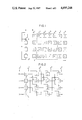
FIG. 3 shows a circuit construction showing an embodiment of the invention, wherein the inputs αi (ao, a1, a2, a3 from the LSB (least significant bit)) are supplied. Coefficients gi of the generator polynomial g(x) are supplied to cascade connected registers 5, 6, 7, and the coefficients g3, g2, g1 are taken from the registers 5, 6, 7. If g(x)=x4 +x+1, it follows that g1 -1, g2 =g3 =0. The coefficient g1 is supplied to AND gates 8, 11, 14, the coefficient g2 is supplied to AND gates 9, 12, 15, and the coefficient g3 is supplied to AND gates 10, 13, 16.
Outputs of the AND gates 8, 9, 10 are supplied to exclusive-OR gates (hereinafter referred to as EXOR gates) 22, 32, 42 respectively at respective first inputs of the EXOR gates. Outputs of the AND gates 11, 12, 13 are supplied to EXOR gates 23, 33, 43 respectively at respective first inputs thereof. Outputs of the AND gates 14, 15, 16 are supplied to EXOR gates 24, 34, 44 respectively at respective first inputs thereof. The respective sets of the three AND gates in each line are commonly supplied with the MSB (most significant bit) from the previous line. The respective sets of the three AND gates in each line always become 0 when the coefficient gi of the generator polynomial is 0, and the former supplies the feedback data to the EXOR gate when the coefficient gi is 1. For example, when g1 =1 and g2 =g3 =0, the EXOR gates 22, 23, 24 act as an adder mod. 2 and other EXOR gates only make the state of the preceding AND gates pass as it is.
Consequently, the MSB in the previous line and outputs of the EXOR gates 22, 23, 24, . . . , 44 constitute all the components of a matrix corresponding to the inputs a0 through a3. Elements (bo, b1, b2, b3) of another field GF(2m) multiplied with the inputs converted into a matrix expression are written in registers 51, 52, 53, 54. The multiplication of the elements (bo, b1, b2, b3,) by the matrix components is represented by ##EQU6## and the outputs co, c1, c2, c3 of the multiplication are as follows: ##EQU7##
The multiplication to generate the output co is executed by AND gates 61, 62, 63, 64, and the addition is executed by EXOR gates 65, 66, 67. The output of the EXOR gate 67 is stored as co in a register 101.
The multiplication to generate the output c1 is executed by AND gates 71, 72, 73, 74, and the addition is executed by EXOR gates 75, 76, 77. The output of the EXOR gate 77 is stored as c1 in a register 102. Similarly, the output c2 formed by AND gates 81, 82, 83, 84 and EXOR gates 85, 86, 87 is stored in a register 103, and the output c3 formed by AND gates 91, 92, 93, 94 and EXOR gates 95, 96, 97 is stored in a register 104.
Thus the circuit shown in FIG. 3 can be used for multiplying the two vectors of the finite field GF(2m) so as to generate a vector product output and change the generator polynomial g(x).
In above-mentioned embodiment of the invention, assume that (ao, a1, a2, a3) is input A, (bo, b1, b2, b3) is input B, and (co, c1, c2, c3) is output C. Then if αN is supplied as input A, output C of αN. B is obtained, wherein N is a value arbitrarily determined among (0, 1, 2, . . . , 2m-2), and αN can be formed by supplying N as the address of a ROM. Similarly, αN can be generated by another ROM so as to form the output C of α-N. B, and further α-i can be generated by another ROM so as to form output C of α-i ·B.
Another embodiment of the invention, shown in FIG. 4, is an arithmetic circuit where a multiplier shown in FIG. 3 is used, and various operations as are described above can be executed without using a ROM.
In FIG. 4, reference numerals 111 and 121 designate converters to convert input data expressed as vectors into components of matrix T, and numerals 112 and 122 designate registers of m bits to store inputs to the converters 111 and 121. The converters 111 and 121 are supplied with coefficients of the generation polynominal from a shift register 117. The shift register 117 executes a shift operation in response to a clock CKG. Numerals 113 and 123 designate multiplication gates to execute matrix multiplication of components of the matrix T from the converters 111 and 121 with data of m bits representing a vector. The multiplication gates 113 and 123 are supplied with data of m bits from registers 114 and 124.
Input data to the register 112 is selected by a multiplexer 115 which is controlled by select signal S1. Input data to the register 114 is selected by a multiplexer 116 which is controlled by select signal S2. Similarly, the registers 122 and 124 are supplied with data selected by multiplexers 125 and 126, respectively. The multiplexers 125 and 126 are controlled by select signals S3 and S4, respectively. The multiplication output of the multiplication gate 113 is supplied to EXOR gate 118; the multiplication output of the multiplication gate 123 is supplied through AND gate 119 to the EXOR gate 118. The AND gate 119 is supplied with a control signal SA, and, if the control signal SA is 1, the addition output (mod. 2) from outputs of both multiplication gates 113 and 123 is taken as output signal C. If the control signal SA is 0, the output of the multiplication gate 113 becomes output signal C.
The multiplexers 115, 116, 125, 126 are supplied with input data of m bits E, A, F, B respectively at data inputs of the multiplexers. The output data C is fed back as additional input data to the multiplexers 115, 116, 125. Further, the multiplication output of the multiplication gate 123 is fed back as additional input data to the multiplexer 126. The output data of the multiplication gate 123 is taken as output data P.
In the arithmetic circuit shown in FIG. 4, the operation mode set by the select signals S1 -S4 and the control signal SA will be described.
First, the operation mode will be described when all select signals S1, S2, S3, S4 are 0 and the control signal SA is 1. Then the input data E, A, F, B are selected by the multiplexers 115, 116, 125, 126 respectively, and the multiplication output of the multiplication gate 123 is supplied through the AND gate 119 to the EXOR gate 118. Consequently, if matrices of the converters 111 and 121 are designated by T1 and T2 respectively, the output data C of (C=T1 A+T2 B) is obtained. If the input data E and F are αi and αj respectively, it follows that T1 =Ti, T2 =Tj. Consequently, the operation
C=T.sup.i ·A+T.sup.j ·B
can be executed. This operation is required in order to implement an error correction circuit.
The operation βN will be described as a second example. Since the number of the power is usually given in binary notation, GF(24) where m=4 will be studied. Then the number of the power N is expressed as follows:
N=n.sub.o ·2.sup.o +n.sub.1 ·2.sup.1 +n.sub.2 ·2.sup.2 n.sub.3 ·2.sup.3
Consequently, the operation βN is executed as follows:
β.sup.N =β.sup.n.sbsp.o.sup.+2n.sbsp.1.sup.+4n.sbsp.2.sup.+8n.sbsp.3
=β.sup.n.sbsp.o ×β.sup.2n.sbsp.1 ×β.sup.4n.sbsp.2 ×β.sup.8n.sbsp.3
wherein no, n1, n2, n3 are 0 or 1. Consequently, β2, β4, β8 may be formed from a given β, and the power operation be executed according to the number of the power.
The procedure during the arithmetic operation of βN will be described referring to FIG. 5. FIG. 5(A) shows clocks of the arithmetic circuit, and the select signals S1 and S2 are 0 during the time t1, t2 as shown in FIG. 5(B) and FIG. 5(C). Data β of four bits is entered as input data E, and αo (=1000) is entered as input data A, F, B. The select signals S1 and S2 become 1 at time t3 and calculation is started.
Input data β and αo are outputted from the multiplexer 115 and 116 as shown in FIG. 5(D) and FIG. 5(E), and these data are outputted from the registers 112 and 114 with a delay of one clock as shown in FIG. 5(F) and FIG. 5(G). At time t3, the output of the register 112 becomes β and the output of the register 114 becomes αo. Since the control signal SA is 0 and output β of the multiplication gate 113 is fed back through the multiplexer 115 and 116 to the registers 112 and 114, the outputs of the registers 112 and 114 become β at time t4. The outputs of the registers 112 and 114 become β2 at time t5, and then vary to β4, β6, β8. FIG. 5(H) shows the output of the multiplication gate 113.
The output of the multiplication gate 113 is supplied through the EXOR gate 118 to the multiplexer 125. Select signal S3 of the multiplexer 125 is changed at every clock corresponding to binary expression of the exponent N (no, n1, n2, n3) as shown in FIG. 5(I). If the select signal S3 is 0, the input data F (=αo) is selected; if the select signal S3 is 1, the output data of the multiplication gate 113 is selected. Consequently, the output of the multiplexer 125 becomes βn.sbsp.o, β2n.sbsp.1, β4n.sbsp.2, β8n.sbsp.3 in sequence as shown in FIG. 5(K), and the output of the register 122 becomes the output of the multiplexer 125 with a delay of one clock as shown in FIG. 5(M).
Select signal S4 becomes 1 at time t4 as shown in FIG. 5(J), and the output of the multiplication gate 123 is selected from input data B (=αo) after time t4. FIG. 5(L) shows the output of the multiplexer 126, and the output of the multiplexer 126 is taken in the register 124 which produces the output shown in FIG. 5(N). At time t4, βn.sbsp.o from the register 122 and αo from the register 124 are supplied to the multiplication gate 123. The output data P of (αo xβn.sbsp.o =βn.sbsp.o) shown in FIG. 5(O) is generated. At time t5, since the input to the multiplication gate 123 becomes β2n.sbsp.1 and β.sup..sbsp.o, the output P of the multiplication gate 123 becomes βn.sbsp.o+2n.sbsp.1. Similarly, corresponding to the input supplied to the multiplication gate 123 at time t6, t7, the output P of βn.sbsp.o+2n.sbsp.1.sup. +4n.sbsp.2+8n.sbsp.3 is obtained from the multiplication gate 123. Although not shown, the output data P is passed through a register and thereby synchronized with the clock and value β8 is outputted at time t8.
The operation mode of β-1 will be described as a third example. In a finite field of GF(24), since an arbitrary element β other than 0 is
β.sup.15 =1
it follows that
β.sup.-1 =β14
That is, N may be made (N=14) and if N=(0111) is inputted as a select signal S3, β-1 is outputted as output data P. In calculating mod. (2m-1), values of N in binary notation may be all converted in order to change N into -N.
In a fourth operation mode of β-N, binary notation of the number of power N may be only converted. Consequently, if β is supplied as input data E and αo is supplied as input data A, F, B, and the converted number of the power N as the select signal S3 is supplied from the LSB in sequence, β-N can be obtained as the output data P.
A fifth operation mode (βN ×γ, β-N ×γ) will be described. This is nearly identical to the second and third operation modes, and γ may be entered as input data B in place of αo.
A sixth operation mode (αi x, α-i x) will be described. In this case, α may be supplied as input data E, αo be supplied as input data A, F and γ be supplied as input data B, and further binary notation data of exponent i or -i be supplied from the LSB in sequence.
As shown in FIG. 6, in order to mutually multiply elements of a finite field GF(24) representing vectors, all components of one element in the matrix expression (16 bits) may be entered from input terminal 131 in series to the shift register circuit, and components of 16 bits be multiplied by the vector (b0, b1, b2, b3). In FIG. 6, each register of the shift register circuit is designated by a suffix of each component of the matrix, and AND gates and EXOR gates to constitute the multiplication gate are designated by reference numerals identical to those in FIG. 3.
Claims (5)
1. An arithmetic circuit comprising:
means for generating as a first input a first set of m bits representing a first vector of a finite field GF(2m) and for generating as a second input a second set of m bits representing a second vector of said finite field;
means for converting said first set of m bits into components of a matrix corresponding to said first vector; and
means for multiplying each of said components by said second set of m bits, thereby to obtain as an output a vector product of said first and second inputs.
2. An arithmetic circuit according to claim 1, in which said converting means comprises a shift register which has a plurality of stages and a feedback loop corresponding to coefficients of a generator polynomial.
3. An arithmetic circuit according to claim 2, in which said converting means further comprises a clock pulse generator, from which a clock pulse is supplied to said shift register, so that a value stored in said shift register is sequentially shifted in response to said clock signal, and means for generating a plurality of outputs from each stage of said shift register at every clock signal to obtain said components.
4. An arithmetic circuit according to claim 3, in which said shift register comprises a plurality of sets of exclusive-OR gates which are connected one after another in such a manner that the exclusive-OR gates of one set produce outputs ranging from a most significant bit to a least significant bit that are respectively applied to one bit higher inputs of the exclusive-OR gates of a following set, and that the most significant bit output of the exclusive-OR gates of said one set becomes a least significant bit input of the exclusive-OR gates of said following set.
5. An arithmetic circuit according to claim 4, in which said multiplying means comprises a plurality of AND gates to which each of said components and each bit of said second set of bits are supplied.
Applications Claiming Priority (2)
| Application Number | Priority Date | Filing Date | Title |
|---|---|---|---|
| JP58-248204 | 1983-12-30 | ||
| JP58248204A JPH0680491B2 (en) | 1983-12-30 | 1983-12-30 | Finite field arithmetic circuit |
Publications (1)
| Publication Number | Publication Date |
|---|---|
| US4697248A true US4697248A (en) | 1987-09-29 |
Family
ID=17174737
Family Applications (1)
| Application Number | Title | Priority Date | Filing Date |
|---|---|---|---|
| US06/685,125 Expired - Lifetime US4697248A (en) | 1983-12-30 | 1984-12-21 | Arithmetic circuit for obtaining the vector product of two vectors |
Country Status (4)
| Country | Link |
|---|---|
| US (1) | US4697248A (en) |
| EP (1) | EP0152702B1 (en) |
| JP (1) | JPH0680491B2 (en) |
| DE (1) | DE3482766D1 (en) |
Cited By (18)
| Publication number | Priority date | Publication date | Assignee | Title |
|---|---|---|---|---|
| US4797848A (en) * | 1986-04-18 | 1989-01-10 | Hughes Aircraft Company | Pipelined bit-serial Galois Field multiplier |
| US4891781A (en) * | 1987-03-04 | 1990-01-02 | Cylink Corporation | Modulo arithmetic processor chip |
| US4918638A (en) * | 1986-10-15 | 1990-04-17 | Matsushita Electric Industrial Co., Ltd. | Multiplier in a galois field |
| US4989171A (en) * | 1988-10-18 | 1991-01-29 | U.S. Philips Corporation | Data processing method and apparatus for calculating a multiplicatively inverted element of a finite field |
| WO1991020028A1 (en) * | 1990-06-15 | 1991-12-26 | Edoardo Mastrovito | Universal galois field multiplier |
| US5165039A (en) * | 1986-03-28 | 1992-11-17 | Texas Instruments Incorporated | Register file for bit slice processor with simultaneous accessing of plural memory array cells |
| US5210710A (en) * | 1990-10-17 | 1993-05-11 | Cylink Corporation | Modulo arithmetic processor chip |
| US5768168A (en) * | 1996-05-30 | 1998-06-16 | Lg Semicon Co., Ltd. | Universal galois field multiplier |
| US5815212A (en) * | 1995-06-21 | 1998-09-29 | Sony Corporation | Video overlay circuit for synchronizing and combining analog and digital signals |
| US20020138534A1 (en) * | 2001-02-08 | 2002-09-26 | Wolfram Drescher | Process and apparatus for finite field multiplication (FFM) |
| GB2389677A (en) * | 2002-06-13 | 2003-12-17 | Guang Yang | A computer method for representing the elements of a binary Galois finite field in the form of a power index array |
| EP1016959A3 (en) * | 1998-12-29 | 2005-07-27 | Texas Instruments Incorporated | Pseudorandom number generator for WCDMA |
| US20060095495A1 (en) * | 2004-10-29 | 2006-05-04 | Choi Yong J | Apparatus for hybrid multiplier in GF(2M) and method thereof |
| EP1449063A4 (en) * | 2001-11-30 | 2006-09-06 | Analog Devices Inc | Galois field multiplier system |
| US20140149479A1 (en) * | 2012-11-29 | 2014-05-29 | Electronics And Telecommunications Research Institute | Method of performing multiplication operation in binary extension finite field |
| US8892495B2 (en) | 1991-12-23 | 2014-11-18 | Blanding Hovenweep, Llc | Adaptive pattern recognition based controller apparatus and method and human-interface therefore |
| US9535563B2 (en) | 1999-02-01 | 2017-01-03 | Blanding Hovenweep, Llc | Internet appliance system and method |
| US10361802B1 (en) | 1999-02-01 | 2019-07-23 | Blanding Hovenweep, Llc | Adaptive pattern recognition based control system and method |
Families Citing this family (5)
| Publication number | Priority date | Publication date | Assignee | Title |
|---|---|---|---|---|
| EP0566215B1 (en) * | 1986-09-30 | 1996-11-20 | Canon Kabushiki Kaisha | Error correction apparatus |
| US5185711A (en) | 1989-12-08 | 1993-02-09 | Sony Corporation | Apparatus for dividing elements of a finite galois field and decoding error correction codes |
| JPH03182122A (en) * | 1989-12-11 | 1991-08-08 | Sony Corp | Division circuit for finite field |
| JPH03179924A (en) * | 1989-12-08 | 1991-08-05 | Sony Corp | Multiplying circuit for finite field |
| US7082452B2 (en) * | 2001-11-30 | 2006-07-25 | Analog Devices, Inc. | Galois field multiply/multiply-add/multiply accumulate |
Citations (4)
| Publication number | Priority date | Publication date | Assignee | Title |
|---|---|---|---|---|
| US4037093A (en) * | 1975-12-29 | 1977-07-19 | Honeywell Information Systems, Inc. | Matrix multiplier in GF(2m) |
| US4251875A (en) * | 1979-02-12 | 1981-02-17 | Sperry Corporation | Sequential Galois multiplication in GF(2n) with GF(2m) Galois multiplication gates |
| US4473887A (en) * | 1981-03-23 | 1984-09-25 | Sony Corporation | Processing circuit for operating on elements of a Galois field |
| US4587627A (en) * | 1981-11-30 | 1986-05-06 | Omnet Associates | Computational method and apparatus for finite field arithmetic |
Family Cites Families (6)
| Publication number | Priority date | Publication date | Assignee | Title |
|---|---|---|---|---|
| US3868632A (en) * | 1972-11-15 | 1975-02-25 | Ibm | Plural channel error correcting apparatus and methods |
| JPS55149551A (en) * | 1979-05-10 | 1980-11-20 | Toshiba Corp | Data correcting circuit |
| JPS5758210A (en) * | 1980-09-26 | 1982-04-07 | Hitachi Ltd | Error correction range controlling circuit |
| EP0096163B1 (en) * | 1982-06-15 | 1988-06-01 | Kabushiki Kaisha Toshiba | Apparatus for dividing the elements of a galois field |
| JPS58219852A (en) * | 1982-06-15 | 1983-12-21 | Toshiba Corp | Correcting circuit of error |
| EP0096165B1 (en) * | 1982-06-15 | 1988-06-08 | Kabushiki Kaisha Toshiba | Apparatus for dividing the elements of a galois field |
-
1983
- 1983-12-30 JP JP58248204A patent/JPH0680491B2/en not_active Expired - Lifetime
-
1984
- 1984-12-21 US US06/685,125 patent/US4697248A/en not_active Expired - Lifetime
- 1984-12-27 DE DE8484309110T patent/DE3482766D1/en not_active Expired - Lifetime
- 1984-12-27 EP EP84309110A patent/EP0152702B1/en not_active Expired - Lifetime
Patent Citations (4)
| Publication number | Priority date | Publication date | Assignee | Title |
|---|---|---|---|---|
| US4037093A (en) * | 1975-12-29 | 1977-07-19 | Honeywell Information Systems, Inc. | Matrix multiplier in GF(2m) |
| US4251875A (en) * | 1979-02-12 | 1981-02-17 | Sperry Corporation | Sequential Galois multiplication in GF(2n) with GF(2m) Galois multiplication gates |
| US4473887A (en) * | 1981-03-23 | 1984-09-25 | Sony Corporation | Processing circuit for operating on elements of a Galois field |
| US4587627A (en) * | 1981-11-30 | 1986-05-06 | Omnet Associates | Computational method and apparatus for finite field arithmetic |
Non-Patent Citations (2)
| Title |
|---|
| Laws, Jr. et al., "A Cellular-Array Multiplier for GF(2m)" IEEE Trans. on Computers, Dec. 1971, pp. 1573-1578. |
| Laws, Jr. et al., A Cellular Array Multiplier for GF(2m) IEEE Trans. on Computers, Dec. 1971, pp. 1573 1578. * |
Cited By (22)
| Publication number | Priority date | Publication date | Assignee | Title |
|---|---|---|---|---|
| US5165039A (en) * | 1986-03-28 | 1992-11-17 | Texas Instruments Incorporated | Register file for bit slice processor with simultaneous accessing of plural memory array cells |
| US4797848A (en) * | 1986-04-18 | 1989-01-10 | Hughes Aircraft Company | Pipelined bit-serial Galois Field multiplier |
| US4918638A (en) * | 1986-10-15 | 1990-04-17 | Matsushita Electric Industrial Co., Ltd. | Multiplier in a galois field |
| US4891781A (en) * | 1987-03-04 | 1990-01-02 | Cylink Corporation | Modulo arithmetic processor chip |
| US4989171A (en) * | 1988-10-18 | 1991-01-29 | U.S. Philips Corporation | Data processing method and apparatus for calculating a multiplicatively inverted element of a finite field |
| WO1991020028A1 (en) * | 1990-06-15 | 1991-12-26 | Edoardo Mastrovito | Universal galois field multiplier |
| US5210710A (en) * | 1990-10-17 | 1993-05-11 | Cylink Corporation | Modulo arithmetic processor chip |
| US8892495B2 (en) | 1991-12-23 | 2014-11-18 | Blanding Hovenweep, Llc | Adaptive pattern recognition based controller apparatus and method and human-interface therefore |
| US5815212A (en) * | 1995-06-21 | 1998-09-29 | Sony Corporation | Video overlay circuit for synchronizing and combining analog and digital signals |
| US5907367A (en) * | 1995-06-21 | 1999-05-25 | Sony Corporation | Video overlay circuit for synchronizing and combining analog and digital signals |
| US5768168A (en) * | 1996-05-30 | 1998-06-16 | Lg Semicon Co., Ltd. | Universal galois field multiplier |
| EP1016959A3 (en) * | 1998-12-29 | 2005-07-27 | Texas Instruments Incorporated | Pseudorandom number generator for WCDMA |
| US10361802B1 (en) | 1999-02-01 | 2019-07-23 | Blanding Hovenweep, Llc | Adaptive pattern recognition based control system and method |
| US9535563B2 (en) | 1999-02-01 | 2017-01-03 | Blanding Hovenweep, Llc | Internet appliance system and method |
| US20020138534A1 (en) * | 2001-02-08 | 2002-09-26 | Wolfram Drescher | Process and apparatus for finite field multiplication (FFM) |
| US7003538B2 (en) * | 2001-02-08 | 2006-02-21 | Systemonic Ag | Process and apparatus for finite field multiplication (FFM) |
| EP1449063A4 (en) * | 2001-11-30 | 2006-09-06 | Analog Devices Inc | Galois field multiplier system |
| GB2389677A (en) * | 2002-06-13 | 2003-12-17 | Guang Yang | A computer method for representing the elements of a binary Galois finite field in the form of a power index array |
| US7599979B2 (en) | 2004-10-29 | 2009-10-06 | Electronics And Telecommunications Research Institute | Apparatus for hybrid multiplier in GF(2m) and method thereof |
| US20060095495A1 (en) * | 2004-10-29 | 2006-05-04 | Choi Yong J | Apparatus for hybrid multiplier in GF(2M) and method thereof |
| US20140149479A1 (en) * | 2012-11-29 | 2014-05-29 | Electronics And Telecommunications Research Institute | Method of performing multiplication operation in binary extension finite field |
| US9311052B2 (en) * | 2012-11-29 | 2016-04-12 | Electronics And Telecommunications Research Institute | Method of performing multiplication operation in binary extension finite field |
Also Published As
| Publication number | Publication date |
|---|---|
| EP0152702B1 (en) | 1990-07-18 |
| DE3482766D1 (en) | 1990-08-23 |
| JPH0680491B2 (en) | 1994-10-12 |
| EP0152702A2 (en) | 1985-08-28 |
| EP0152702A3 (en) | 1986-10-01 |
| JPS60144834A (en) | 1985-07-31 |
Similar Documents
| Publication | Publication Date | Title |
|---|---|---|
| US4697248A (en) | Arithmetic circuit for obtaining the vector product of two vectors | |
| US5185711A (en) | Apparatus for dividing elements of a finite galois field and decoding error correction codes | |
| US4852098A (en) | Polynomial operator in galois fields and a digital signal processor comprising an operator of this type | |
| US5699368A (en) | Error-correcting encoder, error-correcting decoder, and data transmitting system with error-correcting codes | |
| US5446743A (en) | Coefficient updating method and apparatus for Reed-Solomon decoder | |
| US5805617A (en) | Apparatus for computing error correction syndromes | |
| US4797848A (en) | Pipelined bit-serial Galois Field multiplier | |
| KR100309724B1 (en) | Reed solomon coding apparatus and reed solomon coding method | |
| KR100305618B1 (en) | Multipurpose error correction calculation circuit | |
| US6304994B1 (en) | Reed Solomon decoder and decoding method utilizing a control signal indicating a new root for an initial error locator polynomial with respect to new erasure information | |
| JP3279624B2 (en) | 1-bit error correction circuit based on CRC operation | |
| JP2694792B2 (en) | Error position polynomial arithmetic circuit | |
| US4809275A (en) | Parity signal generating circuit | |
| US4368533A (en) | Error data correcting system | |
| US5971607A (en) | Polynomial evaluator for use in a Reed-Solomon decoder | |
| US5448510A (en) | Method and apparatus for producing the reciprocal of an arbitrary element in a finite field | |
| JP3351413B2 (en) | Parallel processing Reed-Solomon encoding circuit and parallel processing Reed-Solomon encoding method used therefor | |
| US6138133A (en) | Circuit for calculating the inverse of an arbitrary element of a finite field | |
| US6145113A (en) | Series reed-solomon decoder synchronized with bit clock signal | |
| US5751732A (en) | Polynomial evaluator for use in a reed-solomon decoder | |
| JPS63107319A (en) | Polynomial division circuit on extended Galois field | |
| JP3131969B2 (en) | Arithmetic unit | |
| JP2570251B2 (en) | Arithmetic circuit of finite field | |
| JP2622957B2 (en) | Coding and decoding method of BCH code | |
| JP2603244B2 (en) | Error correction device |
Legal Events
| Date | Code | Title | Description |
|---|---|---|---|
| AS | Assignment |
Owner name: SONY CORPORATION, 7-35 KITASHINAGAWA-6, SHINAGAWA- Free format text: ASSIGNMENT OF ASSIGNORS INTEREST.;ASSIGNOR:SHIROTA, NORIHISA;REEL/FRAME:004350/0653 Effective date: 19841214 |
|
| STCF | Information on status: patent grant |
Free format text: PATENTED CASE |
|
| FEPP | Fee payment procedure |
Free format text: PAYOR NUMBER ASSIGNED (ORIGINAL EVENT CODE: ASPN); ENTITY STATUS OF PATENT OWNER: LARGE ENTITY |
|
| FPAY | Fee payment |
Year of fee payment: 4 |
|
| FPAY | Fee payment |
Year of fee payment: 8 |
|
| FPAY | Fee payment |
Year of fee payment: 12 |