US4694392A - Video display control - Google Patents
Video display control Download PDFInfo
- Publication number
- US4694392A US4694392A US06/779,819 US77981985A US4694392A US 4694392 A US4694392 A US 4694392A US 77981985 A US77981985 A US 77981985A US 4694392 A US4694392 A US 4694392A
- Authority
- US
- United States
- Prior art keywords
- video
- controller
- processing unit
- central processing
- output
- Prior art date
- Legal status (The legal status is an assumption and is not a legal conclusion. Google has not performed a legal analysis and makes no representation as to the accuracy of the status listed.)
- Expired - Lifetime
Links
Images


Classifications
-
- G—PHYSICS
- G09—EDUCATION; CRYPTOGRAPHY; DISPLAY; ADVERTISING; SEALS
- G09G—ARRANGEMENTS OR CIRCUITS FOR CONTROL OF INDICATING DEVICES USING STATIC MEANS TO PRESENT VARIABLE INFORMATION
- G09G5/00—Control arrangements or circuits for visual indicators common to cathode-ray tube indicators and other visual indicators
- G09G5/001—Arbitration of resources in a display system, e.g. control of access to frame buffer by video controller and/or main processor
-
- G—PHYSICS
- G09—EDUCATION; CRYPTOGRAPHY; DISPLAY; ADVERTISING; SEALS
- G09G—ARRANGEMENTS OR CIRCUITS FOR CONTROL OF INDICATING DEVICES USING STATIC MEANS TO PRESENT VARIABLE INFORMATION
- G09G5/00—Control arrangements or circuits for visual indicators common to cathode-ray tube indicators and other visual indicators
- G09G5/22—Control arrangements or circuits for visual indicators common to cathode-ray tube indicators and other visual indicators characterised by the display of characters or indicia using display control signals derived from coded signals representing the characters or indicia, e.g. with a character-code memory
- G09G5/222—Control of the character-code memory
-
- G—PHYSICS
- G09—EDUCATION; CRYPTOGRAPHY; DISPLAY; ADVERTISING; SEALS
- G09G—ARRANGEMENTS OR CIRCUITS FOR CONTROL OF INDICATING DEVICES USING STATIC MEANS TO PRESENT VARIABLE INFORMATION
- G09G5/00—Control arrangements or circuits for visual indicators common to cathode-ray tube indicators and other visual indicators
- G09G5/36—Control arrangements or circuits for visual indicators common to cathode-ray tube indicators and other visual indicators characterised by the display of a graphic pattern, e.g. using an all-points-addressable [APA] memory
- G09G5/39—Control of the bit-mapped memory
- G09G5/393—Arrangements for updating the contents of the bit-mapped memory
-
- G—PHYSICS
- G09—EDUCATION; CRYPTOGRAPHY; DISPLAY; ADVERTISING; SEALS
- G09G—ARRANGEMENTS OR CIRCUITS FOR CONTROL OF INDICATING DEVICES USING STATIC MEANS TO PRESENT VARIABLE INFORMATION
- G09G2360/00—Aspects of the architecture of display systems
- G09G2360/12—Frame memory handling
- G09G2360/123—Frame memory handling using interleaving
Definitions
- the present invention relates in general to a micro computer system and pertains more particularly to video controller means which form a part of the micro computer system.
- the video controller in accordance with the present invention provides for video display and is capable of both character generation control and cell generation control along with many other forms of control to be described hereinafter.
- an object of the present invention to provide an improved video controller circuit, preferably for use on the micro computer system, and which provides for enhancement of the screen display.
- Another object of the present invention is to provide an improved video controller in accordance with the preceeding objects and in which communication between the central processing unit and the video RAM is accomplished on an interleaved basis which permits during one portion of the cycle screen refresh and during a second portion of the cycle permits a read/write sequence between the central processing unit and the video RAM.
- a video controller preferrably for use in a micro computer system.
- This system includes a video memory means for storing video character codes and including means for controlling writing into and reading from the video memory means.
- This video memory means also has means defining a memory address and memory data.
- a video data bus coupled to the video memory means.
- the central processing unit of the micro computer system has both a data bus and an address bus.
- a cathode ray tube controller means which has address lines coupled therefrom.
- a multiplexer means having first and second input sets and an output set.
- Means are provided for coupling the central processing unit address bus to the first imput set.
- Means are also provided for coupling the cathode ray tube controller means address lines to the second input set.
- means are provided for coupling the output set from the multiplexer means to the video memory means address input.
- Control means are provided for controlling the multiplexer means so that in one state the video memory means is addressed from the cathode ray tube controller means and in the other state the video memory means is addressed from the central processing unit. This occurs on a continuous cyclic basis.
- the central processing unit includes a data bus and video data read latch means coupling from the video data bus to the central processing unit data bus.
- video data write register and means coupling the video data write register from the central processing unit data bus to the video data bus.
- a character generator means coupled from the video output latch means.
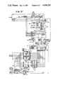
- FIGS. 1A and 1B show one portion of the micro computer system including the basic Z80 processor
- FIGS. 2A, 2B, and 2C show a portion of the micro computer system including programmable array logic (PAL) circuits and decoders used in generating timing signals used in the system;
- PAL programmable array logic
- FIGS. 3A, 3B, and 3C show video circuitry along with the system random access memory and cathode ray tube controller
- FIGS. 4A and 4B show additional timing for the system including keyboard circuitry
- FIGS. 5A and 5B show a portion of the micro computer system including cassette porting
- FIGS. 6A and 6B show a portion of the micro computer system including the video RAM and random access memory timing circuitry
- FIGS. 7-9 show timing diagrams associated with the micro computer system of this invention.
- the video controller of the present invention is preferably adapted for use in a microcomputer which may be of the self-contained desk-top microcomputer type.
- the microcomputer system includes a microprocessor such as the conventional Z-80 microprocessor shown in FIG. 1A which in the microcomputer system of the present invention is capable of running at either of two different clock rates. It also included preferably two programmable array logic (PAL) circuits used for frequency division and routing of appropriate timing signals.
- PAL programmable array logic
- the computer system is provided with main CPU timing from a 20-MHz. clock.
- a first PAL U3 divides the main clock signal by five to provide 4 MHz. CPU operation.
- the main clock is also divided by ten to provide a 2 MHz. rate.
- the logic also waits the CPU at 4 MHz. clock rate for the M1 cycle.
- This first PAL U3 also divides the master clock by four to obtain a 5 MHz. clock to be sent to the RS-232 option connector as a reference for the band rate generator.
- the second PAL U4 selects an appropriate 10 MHz. or 12 MHz. clock video shift clock, and by means of a divider U5, provides additional timing signals to the video display circuitry to be described in further detail hereinafter.
- Low level signals from and to the CPU need to be buffered or current amplified in order to drive many other circuits.
- the 16 address lines are buffered by devices U55 and U66 shown in FIG. 1A, which are uni-directional buffers that are permanently enabled.
- the eight data lines are buffered by device U71. Since data must flow both to and from the CPU, the device U71 is a bi-directional buffer which can go to a three state condition when not in use. Both direction and enable controls come from the address decoding section.
- the clock signal to the CPU is buffered by the active pull-up circuit Q3.
- the RESET and WAIT inputs to the CPU are buffered by gates U17 and U46.
- Control outputs from the Z80 processor include the signals M1--, RD--, WR--, MREQ--and IORQ--. These signals are sent to the PAL U58 shown in FIG. 2A which combine these into other appropriate control signals.
- the raw control signals go to no other components and hence require no additional buffering.
- the address decoding section is divided into two sub-sections, namely port address decoding and memory address decoding.
- port address decoding lower order address lines are sent to the address and enable inputs of decoders U48, U49 nd U50.
- the decoder U48 is also enabled by the signal IN--, which means that it decodes port input signals, while decoder U49 decodes port output signals.
- Memory mapping is accomplished by the PAL U59 shown in FIG. 2A in the basic 16K or 64K system. In a 120K system, the PAL U72 along with the select and memory bit of the option regiser, also enter into the memory mapping function.
- the read-only memory shown in FIG. 1B.
- the ROM is preferably of 14K capacity divided into an 8K ROM, a 4K ROM and a 2K ROM.
- the ROMS that are used preferably have three-state outputs which are disabled if the ROMS are deselected. ROM data outputs are connected directly to the CPU databus.
- the ROMS contain a basic operating system, as well as a floppy disk boot routine.
- the random access memories are available as options in three different capacities including 16K , 64K or 128K of RAM.
- the 16K option uses memory type 4116.
- the 64K and 128K options which are described in detail herein use memory type 6665. This type is of 64K by 1 capacity requiring only a single supply voltage.
- random access memory 10 which is comprises of eight memory units 10-0, 10-1, 10-2, 10-3, 10-4, 10-5, 10-6 and 10-7. Each of these memory units as mentioned previously is of type 6665 having associated therewith input control lines such as lines 12, address lines 14 and output data lines 16. The data outputs from the RAM 10 couple to the databus 18. The databus is identified by the signals D0-D7.
- a dynamic RAM as used herein requires multiplexed incoming address lines. This is accomplished by means of circuits 20 and 22. These circuits are each of type 74157 referred to as quad-multiplexers. The four output lines from the multiplexers 20 and 22 connect by way of resistor array 24 to the address inputs of the RAM. The inputs to the multiplexers 20 and 22 are taken from the address bus 24. The address bus 24 is designated by address lines A0-A15 as noted.
- the random access memory 10 is of conventional design in a readily available circuit chip and has signals coupled thereto such as memory read-write signals and memory request signals. Reference has been made hereinbefore to control lines 12. These include a memory read-write signal (MWR) and a row address strobe signal (RAS). There is also provided as shown at the bottom of the RAM 10 a column address select (CAS).
- MWR memory read-write signal
- RAS row address strobe signal
- CAS column address select
- the data lines 16 from the RAM 10 are coupled to the RAM data buffer 26.
- This buffer may be of type 74LS244 referred to typically as an octal buffer.
- the output of the RAM data buffer 26 couples to the databus and cathode ray tube controller 30.
- the output data lines 27 from the RAM data buffer 26 couple as data signals D0-D7 to the cathode ray tube controller (CRTC) 30.
- the controller 30 is in a sense the heart of the video display circuitry. This controller is of type MC6835.
- the controller 30 allows two screen formats; 64 by 16 and 80 by 24. Since the 80 by 24 screen requires 1,920 screen memory locations, a 2K by 8 static RAM is used for the video RAM.
- the 64 by 16 mode has a two-page screen display and a byte in the options register for determining which page is active for the CPU. One offsets the start address of the controller 30 to gain access to the second page 64 by 16 mode.
- the input control signal on line 32 which is a mode control signal controlling either 64 by 16 or 80 by 24 operation.
- the controller 30 as mentioned previously is a conventional circuit that generates all of the necessary timing and control signals associated with video control including addresses for the video RAM 34.
- the video RAM 34 is of type 4016 and is a 200 nanoseconds RAM of capacity 2K by 8. This is a static RAM.
- the address lines from the controller 30 are coupled in groups to three address multiplexers 36, 38 and 40. These multiplexers are controlled by the CRT clock signal (CRTCLK).
- CRTCLK CRT clock signal
- addresses to the video RAM 34 are provided from the controller 30 when the screen is being refreshed and are provided directly from the CPU by way of the address bus 24 when updating the screen data.
- This alternate control is controlled by the signal CRTCLK which is a bi-level signal that controls the operation.
- This signal CRTCLK is coupled to pin 1 of each of these multiplexers.
- Each of the multiplexers 36, 38 and 40 is referred to as a quad multiplexer of type 74LS157.
- the data lines of the video RAM 34 may be referred to as a video databus 42.
- This video databus intercouples the video RAM with a video data read latch 44, a video data write buffer 46, and a video output latch 48.
- the video data read latch 44 is an octal latch of type 74LS373.
- the video data write buffer 46 is a octal buffer of type 74LS244.
- the video output latch 48 is an octal flip-flop circuit of type 74LS273.
- the data transfer between the CPU and the video RAM 34 is latched by the video data read latch 44 whose output connects to the databus 18. Input data passes to the video data write buffer 46 from the databus 18 to the video RAM.
- the data outputs of the video RAM 34 are latched by the video output latch 48.
- the outputs from the video RAM 34 are ASCII character codes. These data outputs become the addresses for the character generator ROM 50.
- the character generator ROM 50 may be of type MCM68A316E.
- an alternate display in the form of low resolution graphics Accordingly, there is provided a data selector 52 and associated video data output buffer 54.
- the selector 52 may be in the form of a dual multiplexer of type 74LS153.
- the video data output buffer 54 may be a octal buffer of type 74LS244.
- the multiplexer or selector 52 receives the data signals from the video output latch and provides two control signals which are coupled in common separately to the video data output buffer 54.
- the output of the character generator ROM 50 and the video data output buffer 54 couple in common to the shift register 56 which may be of type 74LS166.
- the shift register 56 which may be of type 74LS166.
- the line 58 is the basic video output from the shift register 56.
- the inputs to the shift register 56 are the latched data outputs from either the character generator ROM 50 or the cell generator at the video data output buffer 54.
- the shift clock input on line 57 is a timing signal generated from PAL U4 and is at a frequency of 10.1376 MHz. for the 64 by 16 mode and at a frequency of 12.672 MHz. for the 80 by 24 mode of operation.
- the latch 60 may be a quad flip-flop of type 74LS175. In this regard, it is noted that there are four input data lines and four pairs of output lines including assertion and negation outputs.
- This timing or synchronization provided by the latch 60 includes a blanking control originating from the controller 30 and shift register clocking originating from a PAL of the microcomputer system.
- additional video control and timing functions such as sync buffering, inversion selection, dot clock chopping, and graphics disable of a normal video, are handled by logic gating shown on the drawing and to be soon described.
- Logic set 62 controls, inter alia, the formentioned video inversion.
- INVVIDE inverse video
- the output of the inverter 70 coupled to an AND gate 72.
- the output of the AND gate 72 in turn coupled to a NAND gate 74.
- the logic set 62 also includes NAND gate 75 and AND gate 76.
- the line 66 When the mode of operation is not in inverse video, then the line 66 is low and an enabling signal is coupled by way of the inverter 70 to AND gate 72.
- the other input to the gate 72 is the dataline D7. It is noted that this also couples to one input of the NAND gate 68.
- the logic set 62 also receives the data line signal D6 which it is noted is coupled by way of inverter 75 to one input of the NAND gate 74.
- the output of the gate 74 by way of line 71 couples to a control flip-flop 78.
- the flip-flop 78 has its assertion output coupled by way of line 79 to the buffer 54 and has its negation output coupled by way of line 80 to the character generator ROM 50.
- a load timing signal is coupled to the clock input of the flip-flop 78. This signal is coupled on line 81.
- the flip-flop 78 is set and the low output on line 80 enables the character generator.
- the signal on line 71 is low, this causes a resetting of the flip-flop 78 upon occurrence of the clocking thereof and this causes a low signal on the line 79 for enabling the cell generator section by directly enabling the video data output buffer 54.
- an inversion of the video black-to-white and white-to-black.
- the signal on line 66 is low.
- This signal is inverted by inverter 70 and couples to the AND gate 72 to enable the gate 72.
- the output of the AND gate 72 is also high.
- the output from the gate 72 couples to two different locations. This signal couples directly to the video output latch 48 so as to provide, in normal, non-inverted operation, all eight bytes from the video output latch 48 to the character generator 50.
- the signal from the gate 72 also couples to the NAND gate 74.
- the data line D6 which couples to the inverter 75 has its state establish whether one is generating graphics or characters. For graphics the data bit D6 is low and for characters the data bit D6 is high. Assuming that the data bit D6 is low for graphics, then the inverter 75 causes two high inputs to occur at the gate 74 thus causing a low output therefrom. The output from the gate 74 couples to two different places. The output of this gate couples by way of the aforementioned line 71 to the flip-flop 78 and this output from gate 74 also couples to NAND gate 75. This low level signal at the output of gate 74 provides a high signal at the output of gate 75 and also a high at the output of gate 76.
- the output of gate 76 at line 73 is shown coupling to the latch 60.
- the latch 60 forms a synchronizer providing predetermined delays so that all operations on the character are synchronized at the output video.
- the signal on line 73 entering the latch 60 is delayed at the output line 82.
- This signal couples to the AND gate 83.
- the AND gate 83 also receives on its line 58 the direct character code bits from the shift register 56.
- the output of gate 76 is high and this high level signal, delayed by the latch 60 is coupled to the gate 83.
- the character code bits are capable of passing by way of the gate 84, by way of NAND gate 85 and inverter 86 to the output video line 59.
- the gate 85 has inverted sensing inputs.
- the gate 86 is shown as an exclusive OR gate but is logically an inverter having one of its inputs permanently connected to a voltage high.
- the output on the video line 59 is the dot pattern for generating graphics and characters on a line-by-line basis on the screen at a typical raster scan rate.
- the low output from the gate 74 also couples by way of line 71 to the flip-flop 78 and upon clocking of the flip-flop, it is reset so that the output on the line 79 goes low thus enabling the video data output buffer 54 for enabling data transfer from the cell generator rather than the character generator.
- the high signal on line 80 from the flip-flop 78 causes a disabling of the character generator ROM 50.
- this signal is inverted by the inverter 75 providing a low input to the gate 74 which in turn is inverted by the gate 74 to provide a high output.
- This high output signal from gate 74 couples by way of line 71 to the flip-flop 78 so that upon occurrence of the next clock pulse at line 81, the flip-flop 78 is set, assuming that it had been previously reset.
- the setting of the flip-flop 71 causes a low signal on line 80 for enabling the character generator ROM 50.
- the signal on line 79 from the flip-flop 78 is high and disables the cell generation portion of the circuit or in particular it disables the video data output buffer 54.
- the high output from the gate 74 also couples to the gate 75.
- the other input to gate 75 is the signal RA3 which is a row select signal from the cathode ray tube controller 30.
- This gate 75 is used for blanking to provide a blanking signal between character rows.
- the signal RA3 is high and the output of gate 75 low.
- This low level signal is passed by way of line 73 to the latch 60.
- the delayed signal is coupled by way of line 82 to the gate 83.
- This low level signal inhibits the gate 83.
- the character code bits on line 58 coupled to gate 83 are blanked by virtue of this inhibit signal delayed so as to be properly synchronized by means of the synchronizing latch 60.
- a line intercouples the output of the first flip-flop at output Q1 to the data input 2D of the second flip-flop. It is the output Q2 from the second flip-flop of the latch that couples by way of the line 82 to the AND gate 83.
- the inputs to gate 86 look for low level signals. Thus, when the signal on line 69 is at its high level and when one is not enabling external graphics, then the output of the gate 86 is low. This low level signal is inverted by the gate 88 to a high level signal on line 89. A further inversion occurs in the latch 60 and thus the signal on line 90 is low, thus disabling both sections of the combination AND and NOR gate 92.
- the signal on the line 69 is essentially an inhibiting signal.
- the signal on line 66 goes to its high state.
- this signal couples by way of gate 70 to AND gate 72 to inhibit the gate 72 so that it has a low output.
- This low output is coupled to the video output latch 48 so that the data bit D7 is always at a low state.
- This low level signal also couples to gate 74 so as to provide a high output from gate 74.
- This high output signal from gate 74 couples on line 71 to cause a setting of the flip-flop 78. In this state, the line 80 is low and thus the character generator is enabled.
- the high level signal from NAND gate 74 also couples to the NAND gate 75 and provides operation as previously mentioned for providing blanking between character rows. As indicated previously, this is under control of the signal RA3 from the cathode ray tube controller 30.
- the inverse video signal on line 66 when at its high state, also couples to gate 68 and assuming that the other input to the gate 68 is also high, then the output from 68 goes low.
- This low going signal on line 69 is indicative of character inversion.
- This signal is coupled to gate 86 for causing a high output therefrom which is inverted by gate 88 as long as the display enable signal is present at the other input of the gate.
- This provides a low output signal from the gate 88 which couples to the 3D input of the latch 60. It is noted that the interconnection from the third to the fourth stage is taken at the negation output Q3-- and thus the output at line 90 is a high level signal coupling to the gate 92. for causing enabling thereof.
- the latch 60 as m,entioned previously, is used primarily for synchronization and it is noted that there is a delay provided between the output of the gate 88 and the signal on line 90 coupled to the gate 92. This allows for the proper synchronization between the data presented to the shift register and the occurrence of the inversion signal.
- the signal ENGRAF on line 94.
- This signal couples directly to thegate 92B and also by way of the inverter 87 to the gate 92A.
- the character code bit from gate 83 are essentially overlayed by means of an input graphic control signal referred to as the signal ENGRAF.
- the gate 92B is enabled instead of the gate 92A and as long as the signal GRAFVID is present, then there may be a low signal on line 93 for providing inversion.
- This type of control is possible on a character-by-character basis or bit-by-bit (cell-by-cell) basis.
- OR gate 96 having inverted inputs and AND gate 98.
- One input to the gate 96 is the data line D7.
- the other input to the gate 96 is the signal ENALTSET on line 99.
- this signal on line 99 is present, this signals the generation of an alternate character set from the character generator ROM.
- the alternate character set provides additional characters above the normal characters that are used.
- bits 0-127 represent normal characters
- bits 128-255 represent inverse video characters. If the inverse video signal is low and the alternate set signal is low, then bits 0-127 are normal characters, bits 128-191 are graphics snd bits 192-255 represent a kana character set. If the inverse video signal is low and the alternate character set signal is high, then bits 0-127 are normal characters, bits 128-191 are graphics and bits 192-255 are alternate set characters.
- the output of gate 96 is high and this enables the gate 98.
- the gate 98 is enabled regradless of the state of the signal on the line 97 which is the date line D7.
- the data bit D6 simply passes without inversion through the gate 98 to the corresonding D6 input fothe character generator ROM 50.
- FIGS. 6A and 6B shows the generation of timing signals inconnection with timing for memory access in connection with the microcomputer system.
- the timing control shown in FIG. 16 includes the generation of timing signals fro the random access memory of FIG. 3A as well as timing signals for the video RAM.
- FIG. 3A shows the main memory 10 and the video ram 34.
- the signals that have to do with the timing for the random access memory include the signals SMUX--, RAS--, and ICAS--.
- the timing signals that relate to the video RAM include the signals PWAIT--, OE--, WID--, VBON--, and LATCH DAT--.
- FIGS. 6A and 6B also shows the number of input signals, many of which originate from the central processing unit, which in the preferred embodiment, is a type Z80 processor. Also shown in FIGS. 6A and 6B is part of the circuitry of FIG. 3A shown in block form. This part includes themultiplexer 36 and the video RAM 34. It is the signal identified in FIGS. 6A and 6B as the signal WID-- that is coupled to pin 11 of the multiplexer 36. This is a window signal for providing a window for writing to the the video RAM.
- Read and write signals are coupled directly from the Z80 processor and are identified in FIGS. 6A and 6B as signals ZWR-- and ZRD--. These two signals couple to the gate 110.
- THe output of the gate 110 couples to thedata input of the flip-flop 114.
- the clocking of the flip-flop 114 is from the signal XADR7--. This signal is basically an inversion of the signal CRT CLK shown and discussed in connection with FIG. 3A.
- the clearing of flip-flop 114 is from the signal VIDEO-- by way of the inverter gate 116.
- the signal VIDEO-- also couples to one input of the gate 118 to assert RWAIT--.
- the assertion output of the flip-flop 114 couples to the other input of the gate 118.
- the setting of the flip-flop 114 indicates video access in progress. Since it is known that the video access is now in progress, the signal PWAIT-- is released.
- the output of flip-flop 114 also enables gate 124 and by way of gate 122 starts the timing of the delay line 120.
- the setting of flip-flop 114 occurs upon either a read or write signal from the central processing unit passing by way of the gate 110 with a high level signal at the output thereof for presentation to the flip-flop 114.
- the output signal from gate 118 is the signal PWAIT-- which couples back to the central processing unit. This signal functions as a wait line for the Z80 processor. This action is utilized by the Z80 processor to synchronize to asynchronous signals.
- FIG. 6A also shows a delay line 120 which has an input from the NOR gate 122.
- One input to the gate 122 is the output of flip-flop 114 and the others to the gate 122 is the signal MCYCEN which is a memory cycle enable signal. This is generated through logic from the central processing unit and is for enabling the memory cycle.
- the delay line 120 has a series of taps that provide for different timing functions with different predetermined delays used to carry out controls of the signals particularly for control of the random access memory 10 and the video RAM 34 shown in FIGS. 3A and 3B.
- the gate 118 which generates the signal PWAIT-- is connected so that the signal is present when the signal VIDEO-- occurs but terminates upon the setting of the flip-flop 114. It is noted that the output of the flip-flop 114 also connects to the gate 124.
- the gate 124 is instrumental in control of the video window. While the output of gate 124 is high, the output at inverter 126 is low and this provides one input enable to the gate 128. The other input to the gate 128 is the signal MWR--. If the system is in a write cycle, then the gate 128 is enabled and has a low output. This in turn enables gate 130. This is the signal that is coupled to the multiplexer 36.
- the access in progress signal on line 115 has a line that couples to the NOR gate 122.
- the output of the NOR gate 122 couples to the delay line 120.
- This access in progress signal on line 115 essentially starts the delay line 120 and upon receipt of a low going signal at the pin 12 of the delay 120, the gate 130 is enabled.
- the dispersed output of the delay line 120 is a 30 nanosecond tap.
- the first tap of the delay line essentially starts the video window at the gate 130.
- This signal identified as the signal SMUX-- also couples to gate 136 and provides the video buffer on signal identified as signal VBON--. This is for enabling the video buffer 46, as noted in FIG. 3B. This occurs when the signal WE-- is low.
- the second signal from the delay line at tap 60 is a signal ICAS--.
- the delayed pulse travels down the delay line to the third tap which is tap 150 which couples to a second input of the AND gate 124.
- This low signal provides a high output to pin 4 of gage 130, thus terminating the window signal with the signal WID-- going high. This brings the signal WE-- high and concludes the right cycle to the video ram. This also disables the signal VBON-- which in turn turns off the video buffer 46.
- the signal MWR-- as mentioned previously is instrumental in not only control of the gate 128 but also in generating of the signal OE-- which is the output enable signal for the video RAM 34.
- the gate set 134 also receives the signal CRT CLK and the output therefrom is the aforementioned signal OE--.
- the signal CRT CLK is an alternating signal and depending upon the state thereof, there is essentially an interlacing between control from the cathode ray tube controller (CRTC) 30 or the address lines from the central processing unit (CPU).
- CRTC cathode ray tube controller
- CPU central processing unit
- the address lines are presented from the cathode ray tube controller 30 and the write enable input to the video RAM is held enabled.
- the signal OE-- is also at a state that provides an output enabling of the video RAM.
- the output of the gate set 134 has only one condition that brings its output high and that is when the signal CRT CLK is low and during a write cycle as controlled by the signal MWR--.
- a window is established by the signal WID-- and data is written by way of the video data write buffer 46 into the video RAM 34.
- FIG. 6A also shows additional logic control such as the gate 136 which is used for generating the signal VBON--. As indicated previously, this signal is used in the control of the video data write buffer 46. There is also provided a second gate set 138 that generates at its output the signal RAS--. This signal is used in connection with control of the random access memory shown in FIG. 1.
- the inputs to the gate set 138 are from the tap 300 delay line 120 and also from the signal PRECHG coupled by way of the inverter 139.
- the other input signal to this gate set is the Z80 signal for a memory request, namely signal MREQ. It is noted that the delay line 120 also generates on a properly timed basis, the signal ICAS-- and the signal SMUX-- for the dynamic RAM timing.
- FIG. 6A also shows the generation of the signal WAIT-- from the flip-flop 140. This signal is coupled to the central processing unit and is another one of the WAIT functions for the control of the Z80 processor.
- FIG. 3 With regard to the control in accordance with the present invention, reference is made to FIG. 3 and the video RAM 34 and also to the cathode ray tube controller 30.
- the central processing unit address lines couple to the three multiplexers 36, 38, and 40.
- the control input to each of these multiplexers is at the input pin 1.
- This control is the signal CRT CLK.
- This is an alternating signal which, it is noted, is also coupled to the cathode ray tube controller 30.
- the signal VBON-- enables the video data write buffer and data is written into the video RAM.
- the signal OE-- is high and thus the output of the video RAM is disabled because it is being written into. This control is provided by way of the gate set 134 of FIG. 6A.
Landscapes
- Engineering & Computer Science (AREA)
- Physics & Mathematics (AREA)
- Computer Hardware Design (AREA)
- General Physics & Mathematics (AREA)
- Theoretical Computer Science (AREA)
- Multimedia (AREA)
- Controls And Circuits For Display Device (AREA)
Abstract
Description
Claims (46)
Priority Applications (2)
| Application Number | Priority Date | Filing Date | Title |
|---|---|---|---|
| US06/779,819 US4694392A (en) | 1983-04-27 | 1985-09-25 | Video display control |
| US07/048,906 US4866600A (en) | 1983-04-27 | 1987-05-11 | Computer video control system |
Applications Claiming Priority (2)
| Application Number | Priority Date | Filing Date | Title |
|---|---|---|---|
| US48926283A | 1983-04-27 | 1983-04-27 | |
| US06/779,819 US4694392A (en) | 1983-04-27 | 1985-09-25 | Video display control |
Related Parent Applications (1)
| Application Number | Title | Priority Date | Filing Date |
|---|---|---|---|
| US48926283A Continuation | 1983-04-27 | 1983-04-27 |
Related Child Applications (1)
| Application Number | Title | Priority Date | Filing Date |
|---|---|---|---|
| US07/048,906 Continuation US4866600A (en) | 1983-04-27 | 1987-05-11 | Computer video control system |
Publications (1)
| Publication Number | Publication Date |
|---|---|
| US4694392A true US4694392A (en) | 1987-09-15 |
Family
ID=27049652
Family Applications (1)
| Application Number | Title | Priority Date | Filing Date |
|---|---|---|---|
| US06/779,819 Expired - Lifetime US4694392A (en) | 1983-04-27 | 1985-09-25 | Video display control |
Country Status (1)
| Country | Link |
|---|---|
| US (1) | US4694392A (en) |
Cited By (6)
| Publication number | Priority date | Publication date | Assignee | Title |
|---|---|---|---|---|
| US4860218A (en) * | 1985-09-18 | 1989-08-22 | Michael Sleator | Display with windowing capability by addressing |
| US4866600A (en) * | 1983-04-27 | 1989-09-12 | Tandy Corporation | Computer video control system |
| US4935893A (en) * | 1986-05-30 | 1990-06-19 | International Computers Limited | Data display apparatus |
| US5093902A (en) * | 1987-03-31 | 1992-03-03 | Kabushiki Kaisha Toshiba | Memory control apparatus for accessing an image memory in cycle stealing fashion to read and write videotex signals |
| US5276804A (en) * | 1988-04-27 | 1994-01-04 | Mitsubishi Denki Kabushiki Kaisha | Display control system with memory access timing based on display mode |
| US5742788A (en) * | 1991-07-26 | 1998-04-21 | Sun Microsystems, Inc. | Method and apparatus for providing a configurable display memory for single buffered and double buffered application programs to be run singly or simultaneously |
Citations (5)
| Publication number | Priority date | Publication date | Assignee | Title |
|---|---|---|---|---|
| US3648250A (en) * | 1970-11-13 | 1972-03-07 | Nasa | Digital video display system using cathode-ray tube |
| US4150429A (en) * | 1974-09-23 | 1979-04-17 | Atex, Incorporated | Text editing and display system having a multiplexer circuit interconnecting plural visual displays |
| US4156904A (en) * | 1976-08-25 | 1979-05-29 | Hitachi, Ltd. | Computer systems having a common memory shared between a central processor and a CRT display |
| US4203107A (en) * | 1978-11-08 | 1980-05-13 | Zentec Corporation | Microcomputer terminal system having a list mode operation for the video refresh circuit |
| US4500956A (en) * | 1978-07-21 | 1985-02-19 | Tandy Corporation | Memory addressing system |
-
1985
- 1985-09-25 US US06/779,819 patent/US4694392A/en not_active Expired - Lifetime
Patent Citations (5)
| Publication number | Priority date | Publication date | Assignee | Title |
|---|---|---|---|---|
| US3648250A (en) * | 1970-11-13 | 1972-03-07 | Nasa | Digital video display system using cathode-ray tube |
| US4150429A (en) * | 1974-09-23 | 1979-04-17 | Atex, Incorporated | Text editing and display system having a multiplexer circuit interconnecting plural visual displays |
| US4156904A (en) * | 1976-08-25 | 1979-05-29 | Hitachi, Ltd. | Computer systems having a common memory shared between a central processor and a CRT display |
| US4500956A (en) * | 1978-07-21 | 1985-02-19 | Tandy Corporation | Memory addressing system |
| US4203107A (en) * | 1978-11-08 | 1980-05-13 | Zentec Corporation | Microcomputer terminal system having a list mode operation for the video refresh circuit |
Cited By (6)
| Publication number | Priority date | Publication date | Assignee | Title |
|---|---|---|---|---|
| US4866600A (en) * | 1983-04-27 | 1989-09-12 | Tandy Corporation | Computer video control system |
| US4860218A (en) * | 1985-09-18 | 1989-08-22 | Michael Sleator | Display with windowing capability by addressing |
| US4935893A (en) * | 1986-05-30 | 1990-06-19 | International Computers Limited | Data display apparatus |
| US5093902A (en) * | 1987-03-31 | 1992-03-03 | Kabushiki Kaisha Toshiba | Memory control apparatus for accessing an image memory in cycle stealing fashion to read and write videotex signals |
| US5276804A (en) * | 1988-04-27 | 1994-01-04 | Mitsubishi Denki Kabushiki Kaisha | Display control system with memory access timing based on display mode |
| US5742788A (en) * | 1991-07-26 | 1998-04-21 | Sun Microsystems, Inc. | Method and apparatus for providing a configurable display memory for single buffered and double buffered application programs to be run singly or simultaneously |
Similar Documents
| Publication | Publication Date | Title |
|---|---|---|
| US4663617A (en) | Graphics image relocation for display viewporting and pel scrolling | |
| US5815169A (en) | Frame memory device for graphics allowing simultaneous selection of adjacent horizontal and vertical addresses | |
| US5594473A (en) | Personal computer apparatus for holding and modifying video output signals | |
| US5251298A (en) | Method and apparatus for auxiliary pixel color management using monomap addresses which map to color pixel addresses | |
| US4987551A (en) | Apparatus for creating a cursor pattern by strips related to individual scan lines | |
| CA1253258A (en) | Memory access modes for a video display generator | |
| WO1988000490A1 (en) | Display generator circuitry for personal computer system | |
| KR960013418B1 (en) | Computer video demultiplexer | |
| CA1141021A (en) | Processor for a graphic terminal | |
| US5146211A (en) | Bit mapped color cursor | |
| EP0492840B1 (en) | Videographics display system | |
| US4866600A (en) | Computer video control system | |
| US4694392A (en) | Video display control | |
| EP0215984B1 (en) | Graphic display apparatus with combined bit buffer and character graphics store | |
| JPH05281934A (en) | Data processor | |
| US5230064A (en) | High resolution graphic display organization | |
| US4737780A (en) | Display control circuit for reading display data from a video RAM constituted by a dynamic RAM, thereby refreshing memory cells of the video RAM | |
| US4626839A (en) | Programmable video display generator | |
| US4742342A (en) | Video display generator having alternate display modes | |
| EP0126307A2 (en) | Video controller | |
| EP0126305A2 (en) | Video control system | |
| US5289575A (en) | Graphics coprocessor board with hardware scrolling window | |
| US4646262A (en) | Feedback vector generator for storage of data at a selectable rate | |
| US5694585A (en) | Programmable memory controller and data terminal equipment | |
| EP0148564A2 (en) | High resolution video graphics system |
Legal Events
| Date | Code | Title | Description |
|---|---|---|---|
| STCF | Information on status: patent grant |
Free format text: PATENTED CASE |
|
| FEPP | Fee payment procedure |
Free format text: PAYOR NUMBER ASSIGNED (ORIGINAL EVENT CODE: ASPN); ENTITY STATUS OF PATENT OWNER: LARGE ENTITY |
|
| FPAY | Fee payment |
Year of fee payment: 4 |
|
| REFU | Refund |
Free format text: REFUND OF EXCESS PAYMENTS PROCESSED (ORIGINAL EVENT CODE: R169); ENTITY STATUS OF PATENT OWNER: LARGE ENTITY |
|
| FEPP | Fee payment procedure |
Free format text: PAYER NUMBER DE-ASSIGNED (ORIGINAL EVENT CODE: RMPN); ENTITY STATUS OF PATENT OWNER: LARGE ENTITY Free format text: PAYOR NUMBER ASSIGNED (ORIGINAL EVENT CODE: ASPN); ENTITY STATUS OF PATENT OWNER: LARGE ENTITY |
|
| AS | Assignment |
Owner name: AST RESEARCH, INC., CALIFORNIA Free format text: ASSIGNMENT OF ASSIGNORS INTEREST;ASSIGNOR:TANDY CORPORATION AND ITS RADIO SHACK DIVISION;REEL/FRAME:006847/0109 Effective date: 19940103 |
|
| FPAY | Fee payment |
Year of fee payment: 8 |
|
| AS | Assignment |
Owner name: BANK OF AMERICA NATIONAL TRUST AND SAVINGS ASSOCIA Free format text: SECURITY INTEREST;ASSIGNOR:AST RESEARCH, INC., A DELAWARE CORPORATION;REEL/FRAME:007288/0234 Effective date: 19941223 |
|
| AS | Assignment |
Owner name: AST RESEARCH, INC., CALIFORNIA Free format text: RELEASE BY SECURED PARTY;ASSIGNOR:BANK OF AMERICA NATIONAL TRUST AND SAVINGS ASSOCIATION;REEL/FRAME:007492/0165 Effective date: 19950901 |
|
| FPAY | Fee payment |
Year of fee payment: 12 |
|
| AS | Assignment |
Owner name: SAMSUNG ELECTRONICS CO., LTD., KOREA, REPUBLIC OF Free format text: ASSIGNMENT OF ASSIGNORS INTEREST;ASSIGNOR:AST RESEARCH, INC.;REEL/FRAME:009942/0444 Effective date: 19990421 |
|
| FEPP | Fee payment procedure |
Free format text: PAYOR NUMBER ASSIGNED (ORIGINAL EVENT CODE: ASPN); ENTITY STATUS OF PATENT OWNER: LARGE ENTITY Free format text: PAYER NUMBER DE-ASSIGNED (ORIGINAL EVENT CODE: RMPN); ENTITY STATUS OF PATENT OWNER: LARGE ENTITY |