US4668598A - Multicolor images using an electron beam - Google Patents
Multicolor images using an electron beam Download PDFInfo
- Publication number
- US4668598A US4668598A US06/754,324 US75432485A US4668598A US 4668598 A US4668598 A US 4668598A US 75432485 A US75432485 A US 75432485A US 4668598 A US4668598 A US 4668598A
- Authority
- US
- United States
- Prior art keywords
- film
- electron beam
- pattern
- exposure
- transmitted
- Prior art date
- Legal status (The legal status is an assumption and is not a legal conclusion. Google has not performed a legal analysis and makes no representation as to the accuracy of the status listed.)
- Expired - Fee Related
Links
Images
Classifications
-
- G—PHYSICS
- G03—PHOTOGRAPHY; CINEMATOGRAPHY; ANALOGOUS TECHNIQUES USING WAVES OTHER THAN OPTICAL WAVES; ELECTROGRAPHY; HOLOGRAPHY
- G03G—ELECTROGRAPHY; ELECTROPHOTOGRAPHY; MAGNETOGRAPHY
- G03G5/00—Recording members for original recording by exposure, e.g. to light, to heat, to electrons; Manufacture thereof; Selection of materials therefor
- G03G5/10—Bases for charge-receiving or other layers
- G03G5/104—Bases for charge-receiving or other layers comprising inorganic material other than metals, e.g. salts, oxides, carbon
-
- G—PHYSICS
- G03—PHOTOGRAPHY; CINEMATOGRAPHY; ANALOGOUS TECHNIQUES USING WAVES OTHER THAN OPTICAL WAVES; ELECTROGRAPHY; HOLOGRAPHY
- G03G—ELECTROGRAPHY; ELECTROPHOTOGRAPHY; MAGNETOGRAPHY
- G03G13/00—Electrographic processes using a charge pattern
- G03G13/01—Electrographic processes using a charge pattern for multicoloured copies
-
- G—PHYSICS
- G03—PHOTOGRAPHY; CINEMATOGRAPHY; ANALOGOUS TECHNIQUES USING WAVES OTHER THAN OPTICAL WAVES; ELECTROGRAPHY; HOLOGRAPHY
- G03G—ELECTROGRAPHY; ELECTROPHOTOGRAPHY; MAGNETOGRAPHY
- G03G5/00—Recording members for original recording by exposure, e.g. to light, to heat, to electrons; Manufacture thereof; Selection of materials therefor
- G03G5/12—Recording members for multicolour processes
-
- G—PHYSICS
- G03—PHOTOGRAPHY; CINEMATOGRAPHY; ANALOGOUS TECHNIQUES USING WAVES OTHER THAN OPTICAL WAVES; ELECTROGRAPHY; HOLOGRAPHY
- G03G—ELECTROGRAPHY; ELECTROPHOTOGRAPHY; MAGNETOGRAPHY
- G03G9/00—Developers
- G03G9/08—Developers with toner particles
- G03G9/12—Developers with toner particles in liquid developer mixtures
-
- Y—GENERAL TAGGING OF NEW TECHNOLOGICAL DEVELOPMENTS; GENERAL TAGGING OF CROSS-SECTIONAL TECHNOLOGIES SPANNING OVER SEVERAL SECTIONS OF THE IPC; TECHNICAL SUBJECTS COVERED BY FORMER USPC CROSS-REFERENCE ART COLLECTIONS [XRACs] AND DIGESTS
- Y10—TECHNICAL SUBJECTS COVERED BY FORMER USPC
- Y10S—TECHNICAL SUBJECTS COVERED BY FORMER USPC CROSS-REFERENCE ART COLLECTIONS [XRACs] AND DIGESTS
- Y10S430/00—Radiation imagery chemistry: process, composition, or product thereof
- Y10S430/143—Electron beam
Definitions
- this invention relates to a process for providing direct visual readout in a multicolored format permanently imprinted on a dielectric film which has been exposed to electron beam imaging.
- the invention relates to multicolor imaging of high contrast and definition on a dielectric film and to the product of the multicolored imaging process.
- Previously information received on film from an electron beam source was developed by subjecting the imaged film surface to chemical treatment causing a chemical change in the film composition in order to develop the image for optical readout.
- chemical development in certain cases requires a film having a photographic layer containing a silver halide emulsion which requires photodevelopment to produce a visual black and white image.
- prior practices are restricted to transmittal of the entire pattern or collection of data in a single exposure and provides a format in a single hue or color, e.g. a black on white transparency.
- Another object is to provide a multicolored image. display of an entire pattern or collection of data on a dielectric film imaged by an electron beam source, which image is permanently recorded on said film.
- Still another object is to provide the multicolor image display by an economical and commercially feasible process which avoids variations in the quality of the recorded image.
- a process for producing a multicolored display or readout on a dielectric film imaged by a series of electron beam exposures comprises imaging a dielectric film with a portion of the overall pattern or collection of data to be transmitted by an electrom beam gun, treating the exposed film surface with a colored toner, drying said toner on the surface of the film, re-exposing the film to a second image from said electron beam gun as a second or remaining portion of the overall pattern to be transmitted, treating the resulting re-exposed film surface with a toner of a color distinguished from the first colored toner, drying said second toner on the surface of the film and repeating the above operation, using a toner of distinguishing color after each successive film exposure intended to differentiate the data transmitted, for as many imagings as required to complete the desired pattern or collection of data in contrasting hues or colors.
- the successive images transmitted to the film may be superimposed over the entire film surface or may be recorded on a limited portion of the film by directing the electron beam to a restricted portion of the film.
- the film is preferably composed of at least three distinct layers, namely an electrically resistive dielectric resin layer capable of accepting a colored toner for image development, and having a film thickness of from about 1 to about 10 microns, preferably from about 2 to about 7 microns.
- Suitable resins include organic polymers such as polystyrene, polycarbonate, Teflon, polyethylene, acrylic resins and methacrylic resins.
- This electrically resistive material represents a charge accepting layer which overlays a thin conductive layer having a thickness of between about 0.4 and about 5 microns.
- the conductive layer limits the capacitance of the charge accepting layer and typically has a resistivity of 10 6 ohms/sq. or less.
- the conductive layer is comprised of an electrically conductive metal, metal oxide, metal alloy, metal halide or carbon black, which metal and carbon black components may or may not be suspended in a dispersion medium such as gelatin, dextran, a cellulose ether or ester, etc.
- Suitable metals include gold, silver, platinum, copper, iron, tin, aluminum, indium, nickel, palladium, rhodium, and mixtures thereof.
- Metal oxides which may be suitably employed include indium-tin oxide, copper oxide, iron oxide, etc.
- Silver bromide and copper iodide are illustra-tive of metal halides which are suitably employed for the purposes of this invention.
- the conductive layer is preferably transparent when a clear transparent support is used.
- opaque or translucent supports can tolerate thicker coatings which have reduced transparency.
- a base layer which is a vacuum and dimensionally stable material having low residual volatile gases, liquids and solids.
- An optically clear base layer is preferred and is composed of an organic polymer in a thickness between about 0.25 and about 10 mils.
- Suitable materials employed for the base support layer include polyester, polyethylene terephthalate, clay-sized paper, fiberboard, metal sheet, glazed ceramics, glass, cellulose acetate, polystyrene and polycarbonates.
- Commercially available materials suitable as a base support are, for example, commercial polyester films such as MYLAR film supplied by duPont Corporation and HOSTAPHAN supplied by American Hoechst.
- the separate conductive layer described above can be omitted and the film may comprise only two layers as shown in FIG. 2 of the drawings wherein the electron accepting layer 16 is directly coated on the metal sheet layer 18.
- the metals used for the metal sheet may be any electrically conductive metal such as the metals listed above.
- the multilayered dielectric film is imaged with a portion of the overall pattern or collected data transmitted from an electron beam source.
- the electrons under high vacuum, between about 10 -3 and about 10 31 ] torr, preferably between about 10-5 and about torr, bombard the surface of the film with negative charges, thus transmitting an image thereon for development into an optical display.
- the techniques of electron beam recording are well known, thus further amplification is not required.
- a typical conventional electron beam recording operation suitable for the present invention may utilize an electron beam characterized by having a beam diameter of from about 1 to 25 microns, a voltage of from about 10 to 30 kv., a current flow of from about 10 -] to 10 -6 amps and adapted to scan a target area at a rate such that the dwell time is from about 10 -3 to 10 31 5 seconds.
- Vacuum pressures commonly range from 10 31 3 to 10 -5 torr.
- the image recorded on the surface of the film by the electron beam is then developed by treating the imaged film surface with a toner of a distinctive color and drying the toner on the surface of the film before returning the film for additional image exposure with a further portion or the remaining portion of the pattern to be transmitted.
- the film is treated with a toner of distinguishing color and dried after each image exposure until the complete pattern or collection of data is transmitted and color coded by toner.
- the toners employed for developing the series of images may be selected for contrast, hue and emphasis in the representation appearing on the finished film product.
- These toners are electrographic, color fast, liquids or dispersions or suspensions of fine charged colored particles in a dielectric liquid.
- Preferred toners are those containing organic pigments.
- Representative of the toners which can be employed include those disclosed in British Pat. No. 1,352,067; U.S. Pat. Nos. 3,776,849 and U.S. Pat. No. 3,542,682. In general suitable conventional liquid toners or liquid toners based on toner powders are described on pages 1 and 2 of the British patent.
- liquid toners are those having a disperse pigment phase and a continuous hydrocarbon phase.
- the toners of the British patent are liquid electrostatographic materials having a liquid solvent system, a thermoplastic amphipathic polymer containing a moiety solvated by the system and another non-solvated moiety, and a charge director.
- solvated moieties include:
- Examples of preferred non-solvated moieties include:
- Examples of preferred combinations of solvated and non-solvated moieties in amphipathic polymers include:
- toners reported in U.S. Pat. No. 3,542,682 comprising an electrically insulating carrier liquid, a dispersible coloring agent, such as for example carbon black, alkali blue, nigrosine dyes etc., a soluble metal soap of a fatty acid and an alkylated polymer of a N-vinyl heterocyclic dispersant are also suitably employed herein.
- a dispersible coloring agent such as for example carbon black, alkali blue, nigrosine dyes etc.
- a soluble metal soap of a fatty acid and an alkylated polymer of a N-vinyl heterocyclic dispersant are also suitably employed herein.
- toners of U.S. Pat. No. 3,776,849 comprising a liquid carrier, a pigment and a maleic anhydride copolymer may also be used.
- liquid electrographic toner which is responsive to an electrical image charge
- any liquid electrographic toner which is responsive to an electrical image charge can be employed.
- the above toners are dried on the surface of the film by conventional means, e.g. by air drying or applied heat at a temperature slightly above room temperature up to about 100° C. but below the degradation temperature of the toner and below the distortion temperature of the substrate, for a period of from about 20 seconds to about 5 minutes, preferably from about 1 to about 3 minutes.
- the application of toner can be performed manually by dipping or mechanically by means of a roller, spray etc. in contact with the exposed film surface and is applied in an amount sufficient to provide a clear sharp visual image without tinting the background of the film.
- dielectric film comprising an electron accepting layer of polystyrene (2 microns) overlaying a 0.8 micron layer of indium-tin oxide deposited on a 5 mil polyethylene terephthalate base is exposed to an image relayed from an electron beam gun in a vacuum of 10 -7 torr at room temperature. After imaging, the film is removed and the imaged surface treated with a blue electrographic toner. The toner may be sprayed, dipped or wiped on the surface of the exposed film. After application of the toner, the film is dried at a temperature of 60° C. under atmospheric pressure and subjected to a second image transmitted from the electron beam gun under the above vacuum and temperature conditions.
- the developed film product displays a transmitted pattern wherein the first image is portrayed in a blue reproduction and the second image in a red reproduction of the pattern format.
- the above example illustrates a bicolor representation of the pattern transmitted by an electron beam source.
- more complex representations and displays may be produced in generally the same manner by additional imaging for further information, followed by toning each image in a distinguishing color such as for example magenta, black, green, violet, yellow, etc. and finally drying each toner on the surface of the film for a permanent multicolored finished product.
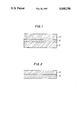
- FIG. 1 represents a vertical cross-sectional view of the preferred product of this invention.
- base support layer 10 over which is coated a thin conductive layer 12 bonded to electron accepting surface layer 14.
- Layer 14 carries the electron beam transmitted pattern in a plurality of colors (not shown).
- FIG. 2 represents a vertical cross-sectional view of film having a copper sheet 18 of from 2 to mil thickness supporting an electron accepting surface layer 16 of from 2 to 10 micron thickness on which toners of distinguishing colors or hues are applied.
- the dielectric film (hereinafter DEF) used for imaging in this example consists of a indium-tin oxide (0.5 microns) coated polyester film of 4 mil thickness supplied by Sierracin Inc., and an overlaying 5 micron dielectric layer of styrenated acrylic resin supplied by Desoto Inc. as Desoto 322.
- a 15 KeV electron beam recorder (hereinafter EBR) operating under a vacuum of 10 - 7 torr was used to image the film in 60 second exposure with a grid pattern.
- EBR KeV electron beam recorder
- the exposed DEF was removed and toned by dipping the imaged film surface into a blue toner (prepared from blue concentrate #6530A, supplied by Philip A. Hunt Corporation by diluting the concentrate 3.2 ml in 800 ml Soltrol*).
- the toner was then air dried on the DEF and the toned film was returned to the EBR where it was exposed under the above conditions to an image of numerical values to be superimposed over the preimaged graph.
- the resulting DEF was again removed from the EBR and dipped with a brown toner (prepared from #6530B concentrate, supplied by Philip A. Hunt Corporation by diluting the concentrate with Soltrol as above).
- the brown toner was then air dried on the film to provide a bicolored film format having an imaged pattern of excellent sharpness and resolution on a transparent colorless film background. After storage of several months, the film product displayed no degradation in heat and light stability.
Abstract
Description
Claims (2)
Priority Applications (7)
| Application Number | Priority Date | Filing Date | Title |
|---|---|---|---|
| US06/754,324 US4668598A (en) | 1985-07-12 | 1985-07-12 | Multicolor images using an electron beam |
| PCT/US1986/001140 WO1987000645A1 (en) | 1985-07-12 | 1986-05-29 | Multicolor images using an electron beam |
| AU59568/86A AU579740B2 (en) | 1985-07-12 | 1986-05-29 | Dielectric multi-color process |
| JP61503240A JPS63500120A (en) | 1985-07-12 | 1986-05-29 | Polychromatic image using electron beam |
| EP19860903897 EP0227741A4 (en) | 1985-07-12 | 1986-05-29 | Multicolor images using an electron beam. |
| IL79080A IL79080A0 (en) | 1985-07-12 | 1986-06-10 | Multicolor images using an electron beam |
| CA000513372A CA1249326A (en) | 1985-07-12 | 1986-07-09 | Multicolor images using an electron beam |
Applications Claiming Priority (1)
| Application Number | Priority Date | Filing Date | Title |
|---|---|---|---|
| US06/754,324 US4668598A (en) | 1985-07-12 | 1985-07-12 | Multicolor images using an electron beam |
Publications (1)
| Publication Number | Publication Date |
|---|---|
| US4668598A true US4668598A (en) | 1987-05-26 |
Family
ID=25034302
Family Applications (1)
| Application Number | Title | Priority Date | Filing Date |
|---|---|---|---|
| US06/754,324 Expired - Fee Related US4668598A (en) | 1985-07-12 | 1985-07-12 | Multicolor images using an electron beam |
Country Status (7)
| Country | Link |
|---|---|
| US (1) | US4668598A (en) |
| EP (1) | EP0227741A4 (en) |
| JP (1) | JPS63500120A (en) |
| AU (1) | AU579740B2 (en) |
| CA (1) | CA1249326A (en) |
| IL (1) | IL79080A0 (en) |
| WO (1) | WO1987000645A1 (en) |
Cited By (3)
| Publication number | Priority date | Publication date | Assignee | Title |
|---|---|---|---|---|
| US5162179A (en) * | 1990-04-17 | 1992-11-10 | Armstrong World Industries, Inc. | Electrographic structure and process |
| EP2407191A1 (en) | 2006-10-30 | 2012-01-18 | Gambro Lundia AB | Air separator extracorporeal fluid treatment sets |
| CN110597422A (en) * | 2019-09-02 | 2019-12-20 | 海宁钟江智能科技有限公司 | Aluminum metal grid capacitor touch film and manufacturing method thereof |
Families Citing this family (1)
| Publication number | Priority date | Publication date | Assignee | Title |
|---|---|---|---|---|
| US4837135A (en) * | 1987-08-13 | 1989-06-06 | E. I. Du Pont De Nemours And Company | Electron beam recording film |
Citations (10)
| Publication number | Priority date | Publication date | Assignee | Title |
|---|---|---|---|---|
| US2883257A (en) * | 1953-05-15 | 1959-04-21 | Bell Telephone Labor Inc | Electron beam recording |
| US3109062A (en) * | 1960-10-27 | 1963-10-29 | Ibm | Electrostatic writing and printing device |
| US3418640A (en) * | 1964-10-22 | 1968-12-24 | Minnesota Mining & Mfg | Method for storing and retrieving information onto and from an electroplatable recording medium |
| US3480459A (en) * | 1965-09-20 | 1969-11-25 | Owens Illinois Inc | Decorating articles utilizing high energy radiation |
| US3653064A (en) * | 1968-02-25 | 1972-03-28 | Canon Kk | Electrostatic image-forming apparatus and process |
| US3757351A (en) * | 1971-01-04 | 1973-09-04 | Corning Glass Works | High speed electostatic printing tube using a microchannel plate |
| US3818493A (en) * | 1972-05-22 | 1974-06-18 | Dyk Res Corp Van | High speed xerographic printer |
| US4378415A (en) * | 1981-10-13 | 1983-03-29 | Xerox Corporation | Color imaging, layered organic photoresponsive device having hole injection and transport layers, red sensitive layer and short wavelength sensitive layer |
| US4510223A (en) * | 1983-02-07 | 1985-04-09 | Coulter Systems Corporation | Multicolor electrophotographic imaging process |
| US4515462A (en) * | 1982-02-26 | 1985-05-07 | Tokyo Shibaura Denki Kabushiki Kaisha | Method and apparatus for forming multicolor image |
Family Cites Families (3)
| Publication number | Priority date | Publication date | Assignee | Title |
|---|---|---|---|---|
| US4006983A (en) * | 1973-10-29 | 1977-02-08 | Electroprint, Inc. | Electrostatic color printing systems using modulated ion streams |
| JPS53110853A (en) * | 1977-03-09 | 1978-09-27 | Matsushita Electric Ind Co Ltd | Color image former |
| JPS58156952A (en) * | 1982-03-15 | 1983-09-19 | Fuji Xerox Co Ltd | Formation of image |
-
1985
- 1985-07-12 US US06/754,324 patent/US4668598A/en not_active Expired - Fee Related
-
1986
- 1986-05-29 AU AU59568/86A patent/AU579740B2/en not_active Ceased
- 1986-05-29 EP EP19860903897 patent/EP0227741A4/en not_active Withdrawn
- 1986-05-29 JP JP61503240A patent/JPS63500120A/en active Pending
- 1986-05-29 WO PCT/US1986/001140 patent/WO1987000645A1/en not_active Application Discontinuation
- 1986-06-10 IL IL79080A patent/IL79080A0/en unknown
- 1986-07-09 CA CA000513372A patent/CA1249326A/en not_active Expired
Patent Citations (10)
| Publication number | Priority date | Publication date | Assignee | Title |
|---|---|---|---|---|
| US2883257A (en) * | 1953-05-15 | 1959-04-21 | Bell Telephone Labor Inc | Electron beam recording |
| US3109062A (en) * | 1960-10-27 | 1963-10-29 | Ibm | Electrostatic writing and printing device |
| US3418640A (en) * | 1964-10-22 | 1968-12-24 | Minnesota Mining & Mfg | Method for storing and retrieving information onto and from an electroplatable recording medium |
| US3480459A (en) * | 1965-09-20 | 1969-11-25 | Owens Illinois Inc | Decorating articles utilizing high energy radiation |
| US3653064A (en) * | 1968-02-25 | 1972-03-28 | Canon Kk | Electrostatic image-forming apparatus and process |
| US3757351A (en) * | 1971-01-04 | 1973-09-04 | Corning Glass Works | High speed electostatic printing tube using a microchannel plate |
| US3818493A (en) * | 1972-05-22 | 1974-06-18 | Dyk Res Corp Van | High speed xerographic printer |
| US4378415A (en) * | 1981-10-13 | 1983-03-29 | Xerox Corporation | Color imaging, layered organic photoresponsive device having hole injection and transport layers, red sensitive layer and short wavelength sensitive layer |
| US4515462A (en) * | 1982-02-26 | 1985-05-07 | Tokyo Shibaura Denki Kabushiki Kaisha | Method and apparatus for forming multicolor image |
| US4510223A (en) * | 1983-02-07 | 1985-04-09 | Coulter Systems Corporation | Multicolor electrophotographic imaging process |
Cited By (4)
| Publication number | Priority date | Publication date | Assignee | Title |
|---|---|---|---|---|
| US5162179A (en) * | 1990-04-17 | 1992-11-10 | Armstrong World Industries, Inc. | Electrographic structure and process |
| EP2407191A1 (en) | 2006-10-30 | 2012-01-18 | Gambro Lundia AB | Air separator extracorporeal fluid treatment sets |
| CN110597422A (en) * | 2019-09-02 | 2019-12-20 | 海宁钟江智能科技有限公司 | Aluminum metal grid capacitor touch film and manufacturing method thereof |
| CN110597422B (en) * | 2019-09-02 | 2023-01-06 | 海宁光圣晶体材料有限公司 | Aluminum metal grid capacitor touch film and manufacturing method thereof |
Also Published As
| Publication number | Publication date |
|---|---|
| WO1987000645A1 (en) | 1987-01-29 |
| AU579740B2 (en) | 1988-12-08 |
| IL79080A0 (en) | 1986-09-30 |
| CA1249326A (en) | 1989-01-24 |
| EP0227741A1 (en) | 1987-07-08 |
| EP0227741A4 (en) | 1987-11-23 |
| JPS63500120A (en) | 1988-01-14 |
Similar Documents
| Publication | Publication Date | Title |
|---|---|---|
| EP0104627B1 (en) | An image receptor and method for producing an opaque print thereon | |
| US3772013A (en) | Photoelectrophoretic imaging process employing electrically photosensitive particles and inert particles | |
| US5176974A (en) | Imaging apparatuses and processes | |
| US3520681A (en) | Photoelectrosolography | |
| US4600669A (en) | Electrophotographic color proofing element and method for using the same | |
| US3512968A (en) | Method of proofing and screening color separations using the manifold imaging process | |
| US3286025A (en) | Recording process using an electron beam to polymerize a record | |
| JP2714456B2 (en) | Manufacturing method of color filter array element by using heated embossed surface | |
| US4006267A (en) | Color highlighting process | |
| US4668598A (en) | Multicolor images using an electron beam | |
| US3236647A (en) | Photographic reproduction process using photopolymerizable resins and new images obtained | |
| US3138458A (en) | Electrophotography | |
| CA1116914A (en) | Electrostatic image forming light transmitting particles containing electrically conductive material and a subliming developing agent | |
| US4654282A (en) | Plural electrophotographic toned image method | |
| US3791823A (en) | Photoelectrophoretic imaging transfer method | |
| US4172721A (en) | Dye-amplified imaging process | |
| US4065307A (en) | Imaged agglomerable element and process of imaging | |
| US3816117A (en) | Multilayer electrophotographic element containing high contrast and opaque barrier layers | |
| US3196765A (en) | Image development and projection | |
| US3967959A (en) | Migration imaging system | |
| JPH0243185B2 (en) | ||
| US4181423A (en) | Electrostatic color printing systems and methods using modulated ion streams | |
| US3198632A (en) | Electrophotography | |
| US4023968A (en) | Photoelectrophoretic color imaging process in which back migration is eliminated | |
| US4006018A (en) | Copying in color |
Legal Events
| Date | Code | Title | Description |
|---|---|---|---|
| AS | Assignment |
Owner name: GAF CORPORATION, 1361 ALPS ROAD, WAYNE, NJ., 07470 Free format text: ASSIGNMENT OF ASSIGNORS INTEREST.;ASSIGNOR:MOSKOWITZ, MARK L.;REEL/FRAME:004668/0567 Effective date: 19850621 Owner name: GAF CORPORATION, A CORP OF DE.,NEW JERSEY Free format text: ASSIGNMENT OF ASSIGNORS INTEREST;ASSIGNOR:MOSKOWITZ, MARK L.;REEL/FRAME:004668/0567 Effective date: 19850621 |
|
| FEPP | Fee payment procedure |
Free format text: PAYOR NUMBER ASSIGNED (ORIGINAL EVENT CODE: ASPN); ENTITY STATUS OF PATENT OWNER: LARGE ENTITY |
|
| AS | Assignment |
Owner name: CHASE MANHATTAN BANK, THE NATIONAL ASSOCIATION Free format text: SECURITY INTEREST;ASSIGNOR:DORSET INC. A CORP OF DELAWARE;REEL/FRAME:005122/0370 Effective date: 19890329 |
|
| AS | Assignment |
Owner name: GAF CHEMICALS CORPORATION Free format text: CHANGE OF NAME;ASSIGNOR:DORSET INC.;REEL/FRAME:005251/0071 Effective date: 19890411 |
|
| FPAY | Fee payment |
Year of fee payment: 4 |
|
| AS | Assignment |
Owner name: DORSET INC., A DE CORP. Free format text: CHANGE OF NAME;ASSIGNOR:GAF CORPORATION, A DE CORP.;REEL/FRAME:005250/0940 Effective date: 19890410 |
|
| AS | Assignment |
Owner name: CHASE MANHATTAN BANK (NATIONAL ASSOCIATION), THE Free format text: SECURITY INTEREST;ASSIGNOR:GAF CHEMICALS CORPORATION, A CORP. OF DE;REEL/FRAME:005604/0020 Effective date: 19900917 |
|
| AS | Assignment |
Owner name: ISP INVESTMENTS INC. Free format text: CHANGE OF NAME;ASSIGNOR:ISP 3 CORP.;REEL/FRAME:005949/0051 Effective date: 19910508 Owner name: ISP 3 CORP Free format text: ASSIGNMENT OF ASSIGNORS INTEREST.;ASSIGNOR:GAF CHEMICALS CORPORATION;REEL/FRAME:005949/0001 Effective date: 19910508 |
|
| AS | Assignment |
Owner name: GAF BUILDING MATERIALS CORPORATION Free format text: RELEASED BY SECURED PARTY;ASSIGNOR:CHASE MANHATTAN BANK, THE (NATIONAL ASSOCIATION);REEL/FRAME:006243/0208 Effective date: 19920804 Owner name: SUTTON LABORATORIES, INC. Free format text: RELEASED BY SECURED PARTY;ASSIGNOR:CHASE MANHATTAN BANK, THE (NATIONAL ASSOCIATION);REEL/FRAME:006243/0208 Effective date: 19920804 Owner name: GAF CHEMICALS CORPORATION Free format text: RELEASED BY SECURED PARTY;ASSIGNOR:CHASE MANHATTAN BANK, THE (NATIONAL ASSOCIATION);REEL/FRAME:006243/0208 Effective date: 19920804 |
|
| REMI | Maintenance fee reminder mailed | ||
| LAPS | Lapse for failure to pay maintenance fees | ||
| FP | Lapsed due to failure to pay maintenance fee |
Effective date: 19950531 |
|
| STCH | Information on status: patent discontinuation |
Free format text: PATENT EXPIRED DUE TO NONPAYMENT OF MAINTENANCE FEES UNDER 37 CFR 1.362 |