US4616406A - Process of making a semiconductor device having parallel leads directly connected perpendicular to integrated circuit layers therein - Google Patents
Process of making a semiconductor device having parallel leads directly connected perpendicular to integrated circuit layers therein Download PDFInfo
- Publication number
- US4616406A US4616406A US06/655,476 US65547684A US4616406A US 4616406 A US4616406 A US 4616406A US 65547684 A US65547684 A US 65547684A US 4616406 A US4616406 A US 4616406A
- Authority
- US
- United States
- Prior art keywords
- die
- pins
- array
- parallel
- leads
- Prior art date
- Legal status (The legal status is an assumption and is not a legal conclusion. Google has not performed a legal analysis and makes no representation as to the accuracy of the status listed.)
- Expired - Lifetime
Links
Images


Classifications
-
- H—ELECTRICITY
- H10—SEMICONDUCTOR DEVICES; ELECTRIC SOLID-STATE DEVICES NOT OTHERWISE PROVIDED FOR
- H10W—GENERIC PACKAGES, INTERCONNECTIONS, CONNECTORS OR OTHER CONSTRUCTIONAL DETAILS OF DEVICES COVERED BY CLASS H10
- H10W99/00—Subject matter not provided for in other groups of this subclass
-
- H—ELECTRICITY
- H10—SEMICONDUCTOR DEVICES; ELECTRIC SOLID-STATE DEVICES NOT OTHERWISE PROVIDED FOR
- H10W—GENERIC PACKAGES, INTERCONNECTIONS, CONNECTORS OR OTHER CONSTRUCTIONAL DETAILS OF DEVICES COVERED BY CLASS H10
- H10W74/00—Encapsulations, e.g. protective coatings
- H10W74/01—Manufacture or treatment
-
- H—ELECTRICITY
- H10—SEMICONDUCTOR DEVICES; ELECTRIC SOLID-STATE DEVICES NOT OTHERWISE PROVIDED FOR
- H10W—GENERIC PACKAGES, INTERCONNECTIONS, CONNECTORS OR OTHER CONSTRUCTIONAL DETAILS OF DEVICES COVERED BY CLASS H10
- H10W74/00—Encapsulations, e.g. protective coatings
- H10W74/10—Encapsulations, e.g. protective coatings characterised by their shape or disposition
- H10W74/111—Encapsulations, e.g. protective coatings characterised by their shape or disposition the semiconductor body being completely enclosed
-
- Y—GENERAL TAGGING OF NEW TECHNOLOGICAL DEVELOPMENTS; GENERAL TAGGING OF CROSS-SECTIONAL TECHNOLOGIES SPANNING OVER SEVERAL SECTIONS OF THE IPC; TECHNICAL SUBJECTS COVERED BY FORMER USPC CROSS-REFERENCE ART COLLECTIONS [XRACs] AND DIGESTS
- Y10—TECHNICAL SUBJECTS COVERED BY FORMER USPC
- Y10T—TECHNICAL SUBJECTS COVERED BY FORMER US CLASSIFICATION
- Y10T29/00—Metal working
- Y10T29/49—Method of mechanical manufacture
- Y10T29/49002—Electrical device making
- Y10T29/49117—Conductor or circuit manufacturing
- Y10T29/49169—Assembling electrical component directly to terminal or elongated conductor
- Y10T29/49171—Assembling electrical component directly to terminal or elongated conductor with encapsulating
- Y10T29/49172—Assembling electrical component directly to terminal or elongated conductor with encapsulating by molding of insulating material
Definitions
- This invention relates to packaging of semiconductor devices. More particularly, this invention relates to a semiconductor device having an array of parallel leads directly bonded to the integrated circuit die perpendicular to the die layers.
- Typical prior art lead packages for semiconductor devices comprise the so-called dual in-line type packages wherein the die is bonded face up to a mounting pad and peripheral leads, located parallel to the plane of the die and mounting pad, are connected to contact pads, such as shown in Denlinger et al U.S. Pat. No. 4,173,768, on opposite edges on the die. The device is then encapsulated in plastic and the lead ends are bent perpendicular to the device. Duffek et al U.S. Pat. No. 3,947,867 illustrates such devices.
- Such lead packages may include the provision of leads on all four edges of the die when further lead connections are needed.
- Typical lead packages of this sort are illustrated in Hayakawa et al U.S. Pat. No. 4,280,132; Burns U.S. Pat. No. 4,330,790; Brown U.S. Pat. No. 4,400,714; Grabbe U.S. Pat. No. 4,408,218; and Chiba et al U.S. Pat. No. 4,415,917.
- Another packaging technique involves the so-called “flip chip” approach wherein the die is bonded face down to an insulative substrate as shown in Hantusch U.S. Pat. No. 4,288,808 and Test U.S. Pat. No. 4,423,435.
- This approach has been described, in connection with the use of spring loaded cooling pistons applied to the backside of the die, by Blodgett in "Microelectronic Packaging” in volume 249 of Scientific American (July, 1983) at pages 86-89.
- the author describes a package termed a module which may have as many as 100 to 133 high speed chips bonded by the "flip chip” method to a substrate comprising 33 conductive layers which, together with a grid of vias, interconnect the dies together.
- a grid of pins or leads is brazed perpendicular to the opposite surface of the substrate to provide interconnection of the module to other electrical devices.
- It is another object of this invention to provide an improved semiconductor package comprising an integrated circuit die and a mounting package which includes an array of leads mounted perpendicular to the plane of the die.
- It is yet another object of this invention to provide and improved semiconductor package comprising an integrated circuit die and a mounting package which includes an array of leads mounted perpendicular to the plane of the die and bonded directly to the die.
- an improved semiconductor device comprises an integrated circuit die having directly mounted to contacts thereon an orthogonal array of parallel leads perpendicular to the die.
- the die and leads are mounted in a package material to protect the die as well as to assist in maintaining the alignment of the array of leads.
- the array of parallel leads is arranged in a hexagonal spacing rather than orthogonal to provide a higher lead density.
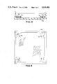
- FIG. 1 is an isometric view of one embodiment of the semiconductor package of the invention.
- FIG. 2 is a side section view of a jig used in forming the array of leads.
- FIG. 3 is a side section view of one embodiment of the invention.
- FIG. 4 is a side section exploded view illustrating an alternate method of construction.
- FIG. 5 is a side section view of a potting shell utilized in the invention.
- FIG. 6 is a top view of the potting shell of FIG. 5.
- FIG. 7 is a side section view of a semiconductor package made in accordance with the invention utilizing the potting shell shown in FIGS. 5 and 6.
- FIG. 8 is a top view of the lead arrangement of one embodiment of the invention.
- FIG. 9 is a top view of the lead arrangement of another embodiment of the invention.
- the improved semiconductor package of the invention is generally illustrated at 2.
- the package comprises an array of parallel, equally spaced apart, leads 14 which are bonded directly, and perpendicularly, to the integrated circuit die (not shown) within packaging material 12.
- the advantages of the package construction of the invention include high density spacing of leads for maximizing of board space utilization; ease of assembly of the finished package on the PC board using present chip carrier pick and place tooling to handle the assembly; and the assembly of leads and dies for different lead counts using the same tools--resulting in lower tooling costs, i.e., no lead frame tooling for every lead count.
- the advantages of the package of the invention include shorter traces on the PC board resulting in less loading of signals, faster switching, etc.; lower circuit board costs per function; lower lead inductance and capacitance; and good match of electrical parameters between pins or leads because of their uniform lengths.
- the package of the invention also possesses improved thermal characteristics with good thermal conductivity through the leads to the PC board and no thermal coefficient of expansion mismatch problems.
- one of the characteristics of the invention is the improved lead density.
- a 289 lead count surface mountable package would only require 0.3 square inches with the leads mounted on 25 mil centers while an equivalent prior art plastic leaded chip carrier having 25 mil center lead spacing would require 3.5 square inches, and a standard 50 mil center plastic leaded chip carrier would require 13.0 square inches.
- Package 2 as illustrated in FIG. 1 after molding in plastic would, in contrast, have exterior dimensions of only 0.55" ⁇ 0.55" ⁇ 0.1". As will be discussed below, even higher density of leads spacing is possible using one embodiment of the invention.
- the package of the invention is also characterized by improved heat dissipation.
- the heat dissipation for the package can be calculated as:
- the heat dissipation would equal 0.45299. If the device dissipates 10 watts, then the junctions would be 4.5° C. higher than the traces to which they are connected. This heat would be transferred to the copper traces on the PC board. Depending on the thickness of the laminates and the copper traces, the heat dissipation will vary.
- the best interconnect substrate would be an aluminum backed flex circuit. The heat would then go through perhaps 25 mils of polymer to an aluminum heat sink.
- Package 2 may be constructed by first placing the leads 14 into a grid workholder or jig 20 which will hold the array of leads in a parallel, equally spaced apart, arrangement with all the leads of even height for subsequent attachment thereto of the die.
- workholder or jig 20 is comprised of a three layered laminated device comprising ceramic layers 22, 24, and 26.
- Layers 24 and 26 are drilled precisely with a laser to provide, in each layer, a precise array of parallel, equally spaced apart, bores. In the preferred embodiment, eleven mil diameter holes are drilled on a spacing of 25 mils apart.
- Ceramic substrate layers 24 and 26 are preferably about 25 mils thick and, after drilling, are stacked back to back with the wider ends of the respective holes or bores 28a and 28b facing each other. Undrilled ceramic layer or substrate 22 is then attached to one side and the three layers or substrates are laminated together with adhesive to form the completed workholder or jig 20.
- the conical shape of the bore or hole drilled in each of the ceramic layers plus the bonding together of the two substrates to place the wider portions of the bores 28a and 28b in the middle of bore 28 permits jig or workholder 20 to hold each of the leads precisely perpendicular without providing undue friction or drag on the lead when the array of leads are subsequently removed from the jig or workholder after the lead array has been bonded together to form a unit as will be described below.
- each lead is placed in a hole or bore 28 in workholder 20 and cut off with a laser precisely 10 mils above the surface of workholder 20.
- the leads may be formed by winding off 10 mil diameter copper wire from a spool while the workholder is sitting on XY table so that it may be indexed to the next array location to permit the accurate, yet automatic, filling of workholder 20 with leads 14.
- die 10 may be attached to the array by placing it face down on the wires.
- Die 10 is preferably provided with a grid array top metallization layer similar to a "flip chip” or “bump chip” with high temperature solder at each of the contact pads in registry with the lead array in advance of the connection.
- the array of leads may be presoldered using a roller carrying high temperature solder paste that is passed over the tips of the leads while they are held in grid workholder 20.
- Die 10 is then placed or positioned on the array of leads by precisely aligning the edges of workholder 20 with the edges of die 10, and the solder is reflowed to attach the leads to the die with hot nitrogen or forming gas to melt the high temperature solder.
- the assembly is then removed from workholder 20, placed into a mold, and plastic is poured around the die and the array of leads attached thereto to form package 2 shown in FIG. 3.
- the flash is removed by mild abrasion on the bottom of the leads. Since there is no lead trim and form operation, however, the cost is reduced and the reliability is improved since lead trim and form creates cracks along the plastic/lead frame interface.
- the resulting package 2 comprises plastic material 12 surrounding die 10 and leads 14.
- Package 2 is also provided with standoffs 34 which protrude approximately 15 mils from the bottom of package 2.
- Standoffs 34 which may be located on the four corners of package 2, have a predetermined cross-section which will, in turn, lock into a mating pattern on a copper trace of the PC board to which package 2 will be ultimately attached. This will assure good alignment between leads 14 and the contact pads on the PC board.
- the traces on a PC board usually sit 3 mils higher than the base laminate leaving a 2 mil gap which would be taken up by reflow solder.
- Standoffs 34 may be all of the same cross-section or they may have different cross-sections to assure that package 2 may only be mounted or oriented in one way on the PC board to prevent improper connection of package 2 to the PC board.
- additional conducting layers may be placed on the die.
- the die could be first patterned with a polymer dielectric, such as a polyimide, and metal traces to bring the signals from existing bond pads on the perimeter of the die to the respective lead array sites.
- Another dielectric layer would then be added with vias and then the final lead attach pad metallized on top. While some of the electrical and thermal advantages of the invention, such as shorter lead length, etc., would not be realized in this construction, it would permit the interim use of conventional dies without complete redesign of the die layout. New die layouts would, of course, be designed to take maximum advantage of the direct lead connection possible in the practice of this invention.
- FIG. 4 an alternate embodiment is shown in which the array of leads is first surrounded by packaging material 12' prior to attachment of die 10 thereto.
- a premolded carrier may be back filled with epoxy.
- the premolded carrier could be made of metal with glass insulation around each lead going through a drilled hole.
- the package may be completed using conventional techniques for either hermetic or nonhermetic packaging as is well known to those skilled in the art.
- FIGS. 5-7 a preferred embodiment is shown in which the partially assembled package having the die 10 attached to leads 14 is placed in a potting shell 50.
- Standoff hemispherical bumps or spacers 52 are provided on the inside of the bottom wall of potting shell 50 to space die 10 from the bottom of potting shell 50 for a purpose to be described below.
- Hemicylindrical guides 54 are located on the side walls of potting shell 50 to assure proper positioning of die 10.
- Potting shell 50 may then be partially filled with an elastomeric silicon die gel 42. Die 10 is then placed in potting shell 50 positioned therein from the bottom and sidewalls, respectively, by hemispherical standoffs 52 and hemicylindrical guides 54. Potting shell 50 is then partially backfilled with more gel, cured, and then topped off with a potting solution 44. This, then, permits die 10 in potting shell 50 to be "floating" in a low stress situation. This type of arrangement allows outside dimensions of the potting shells to be standardized with different size guides and standoffs within the potting shell to permit the use of different size dies therein.
- package 2 in FIG. 8 illustrates placement of the leads in an array wherein equally spaced apart rows or columns configure the leads into a square or "orthogonal" arrangement as previously discussed with respect to FIG. 1. While this arrangement of the leads will provide a lead density far in excess of that now used in standard packages wherein the leads are placed around two or four edges of the package, the arrangement of leads 14 in package 2' shown in FIG. 9 will provide yet an even higher density by placing the leads in a triangle or hexagonal spacing.
- a 289 lead count surface mountable package with leads located on 25 mil centers would require 0.3 square inches.
- the same number of leads can be placed in approximately 87% of the space used by the same orthogonal array. This number is approximately the sine of 60°. This smaller spacing permits a package of the same size to have 320 connections rather than 289 using orthogonal spacing.
- the use of the preferred hexagonal spacing also improves the electrical characteristics of the package as well as increasing the number of leads which can be used in a given area for a given lead spacing.
- the axes of the leads would be 120° apart on a plane. Since one could go in a negative as well as a positive direction, one has a choice of routing a signal from a single contact in six different directions set at 60° apart rather than four at 90°. This leads to calculating the worst case routing situation as one 30° away from two of the six directions. This leads the path to be ⁇ 4/3 times longer than a direct path, compared to ⁇ 2 times longer for the orthogonal system. Since system speed is determined by the worst case, the hexagonal system is 20% faster.
- the invention provides an improved semiconductor package wherein the number of leads which may be attached to an integrated circuit die is radically increased without, however, increasing the overall size of the package by providing a preselected density of leads in an array of parallel and equally spaced apart leads which are then mounted directly to the die perpendicular to the plane of the die.
Landscapes
- Lead Frames For Integrated Circuits (AREA)
- Structures Or Materials For Encapsulating Or Coating Semiconductor Devices Or Solid State Devices (AREA)
- Coupling Device And Connection With Printed Circuit (AREA)
- Internal Circuitry In Semiconductor Integrated Circuit Devices (AREA)
- Ladders (AREA)
Abstract
Description
Claims (12)
Priority Applications (5)
| Application Number | Priority Date | Filing Date | Title |
|---|---|---|---|
| US06/655,476 US4616406A (en) | 1984-09-27 | 1984-09-27 | Process of making a semiconductor device having parallel leads directly connected perpendicular to integrated circuit layers therein |
| AT85306859T ATE59733T1 (en) | 1984-09-27 | 1985-09-26 | A METHOD OF MAKING A SEMICONDUCTOR DEVICE WITH CONDUCTOR PINS. |
| DE8585306859T DE3581049D1 (en) | 1984-09-27 | 1985-09-26 | A METHOD FOR PRODUCING A SEMICONDUCTOR ARRANGEMENT WITH LADDER PLUGS. |
| EP85306859A EP0179577B1 (en) | 1984-09-27 | 1985-09-26 | Method for making a semiconductor device having conductor pins |
| JP60214435A JPS6184854A (en) | 1984-09-27 | 1985-09-26 | Manufacture of semiconductor device and semiconductor package |
Applications Claiming Priority (1)
| Application Number | Priority Date | Filing Date | Title |
|---|---|---|---|
| US06/655,476 US4616406A (en) | 1984-09-27 | 1984-09-27 | Process of making a semiconductor device having parallel leads directly connected perpendicular to integrated circuit layers therein |
Publications (1)
| Publication Number | Publication Date |
|---|---|
| US4616406A true US4616406A (en) | 1986-10-14 |
Family
ID=24629033
Family Applications (1)
| Application Number | Title | Priority Date | Filing Date |
|---|---|---|---|
| US06/655,476 Expired - Lifetime US4616406A (en) | 1984-09-27 | 1984-09-27 | Process of making a semiconductor device having parallel leads directly connected perpendicular to integrated circuit layers therein |
Country Status (5)
| Country | Link |
|---|---|
| US (1) | US4616406A (en) |
| EP (1) | EP0179577B1 (en) |
| JP (1) | JPS6184854A (en) |
| AT (1) | ATE59733T1 (en) |
| DE (1) | DE3581049D1 (en) |
Cited By (32)
| Publication number | Priority date | Publication date | Assignee | Title |
|---|---|---|---|---|
| US4820976A (en) * | 1987-11-24 | 1989-04-11 | Advanced Micro Devices, Inc. | Test fixture capable of electrically testing an integrated circuit die having a planar array of contacts |
| US4916523A (en) * | 1988-09-19 | 1990-04-10 | Advanced Micro Devices, Inc. | Electrical connections via unidirectional conductive elastomer for pin carrier outside lead bond |
| US4916522A (en) * | 1988-04-21 | 1990-04-10 | American Telephone And Telegraph Company , At & T Bell Laboratories | Integrated circuit package using plastic encapsulant |
| US5135890A (en) * | 1989-06-16 | 1992-08-04 | General Electric Company | Method of forming a hermetic package having a lead extending through an aperture in the package lid and packaged semiconductor chip |
| US5541449A (en) * | 1994-03-11 | 1996-07-30 | The Panda Project | Semiconductor chip carrier affording a high-density external interface |
| US5543586A (en) * | 1994-03-11 | 1996-08-06 | The Panda Project | Apparatus having inner layers supporting surface-mount components |
| US5576931A (en) * | 1994-05-03 | 1996-11-19 | The Panda Project | Computer with two fans and two air circulation areas |
| US5575688A (en) * | 1992-12-01 | 1996-11-19 | Crane, Jr.; Stanford W. | High-density electrical interconnect system |
| US5634821A (en) * | 1992-12-01 | 1997-06-03 | Crane, Jr.; Stanford W. | High-density electrical interconnect system |
| US5691569A (en) * | 1995-12-20 | 1997-11-25 | Intel Corporation | Integrated circuit package that has a plurality of staggered pins |
| US5801421A (en) * | 1995-11-13 | 1998-09-01 | Micron Technology, Inc. | Staggered contact placement on CMOS chip |
| US5812797A (en) * | 1994-03-11 | 1998-09-22 | The Panda Project | Computer having a high density connector system |
| US5821457A (en) * | 1994-03-11 | 1998-10-13 | The Panda Project | Semiconductor die carrier having a dielectric epoxy between adjacent leads |
| US5819403A (en) * | 1994-03-11 | 1998-10-13 | The Panda Project | Method of manufacturing a semiconductor chip carrier |
| US5824950A (en) * | 1994-03-11 | 1998-10-20 | The Panda Project | Low profile semiconductor die carrier |
| US5909010A (en) * | 1996-08-21 | 1999-06-01 | Nec Corporation | Chip size package |
| US5937276A (en) * | 1996-12-13 | 1999-08-10 | Tessera, Inc. | Bonding lead structure with enhanced encapsulation |
| US6078102A (en) * | 1998-03-03 | 2000-06-20 | Silicon Bandwidth, Inc. | Semiconductor die package for mounting in horizontal and upright configurations |
| US6141869A (en) * | 1998-10-26 | 2000-11-07 | Silicon Bandwidth, Inc. | Apparatus for and method of manufacturing a semiconductor die carrier |
| US6229209B1 (en) | 1995-02-23 | 2001-05-08 | Matsushita Electric Industrial Co., Ltd. | Chip carrier |
| US6307258B1 (en) | 1998-12-22 | 2001-10-23 | Silicon Bandwidth, Inc. | Open-cavity semiconductor die package |
| US20020014004A1 (en) * | 1992-10-19 | 2002-02-07 | Beaman Brian Samuel | High density integrated circuit apparatus, test probe and methods of use thereof |
| US6384477B2 (en) * | 1997-04-26 | 2002-05-07 | Glotech Inc. | Multiple line grid array package |
| US6397460B1 (en) | 1999-03-10 | 2002-06-04 | Micron Technology, Inc. | Electrical connector |
| US20020093351A1 (en) * | 2001-01-18 | 2002-07-18 | Holcombe Brent A. | Method for constructing a flex-rigid laminate probe |
| US6448106B1 (en) * | 1999-11-09 | 2002-09-10 | Fujitsu Limited | Modules with pins and methods for making modules with pins |
| US6472724B1 (en) * | 1999-04-19 | 2002-10-29 | Nec Corporation | Electronic device structure capable of preventing malfunction caused by electromagnetic wave coming from outside |
| US20040158979A1 (en) * | 1996-07-09 | 2004-08-19 | Takaaki Higashida | Method of manufacturing a semiconductor element-mounting board |
| US6830177B2 (en) * | 2001-09-10 | 2004-12-14 | General Dynamics Information Systems, Inc. | Method and apparatus to compliantly interconnect commercial-off-the-shelf chip scale packages and printed wiring boards |
| US20050062492A1 (en) * | 2001-08-03 | 2005-03-24 | Beaman Brian Samuel | High density integrated circuit apparatus, test probe and methods of use thereof |
| US20110204508A1 (en) * | 2010-02-22 | 2011-08-25 | In Sang Yoon | Semiconductor packaging system with an aligned interconnect and method of manufacture thereof |
| CN116117266A (en) * | 2022-12-23 | 2023-05-16 | 北京卫星制造厂有限公司 | Micro-spring pin quick assembly tool and method for integrated circuit |
Families Citing this family (3)
| Publication number | Priority date | Publication date | Assignee | Title |
|---|---|---|---|---|
| US5260601A (en) * | 1988-03-14 | 1993-11-09 | Texas Instruments Incorporated | Edge-mounted, surface-mount package for semiconductor integrated circuit devices |
| US4975763A (en) * | 1988-03-14 | 1990-12-04 | Texas Instruments Incorporated | Edge-mounted, surface-mount package for semiconductor integrated circuit devices |
| CN114999930B (en) * | 2022-05-25 | 2025-08-19 | 西安微电子技术研究所 | Appearance processing method of epoxy resin encapsulated circuit |
Citations (6)
| Publication number | Priority date | Publication date | Assignee | Title |
|---|---|---|---|---|
| US3273029A (en) * | 1963-08-23 | 1966-09-13 | Hoffman Electronics Corp | Method of attaching leads to a semiconductor body and the article formed thereby |
| US4074342A (en) * | 1974-12-20 | 1978-02-14 | International Business Machines Corporation | Electrical package for lsi devices and assembly process therefor |
| US4196444A (en) * | 1976-12-03 | 1980-04-01 | Texas Instruments Deutschland Gmbh | Encapsulated power semiconductor device with single piece heat sink mounting plate |
| US4312116A (en) * | 1980-04-14 | 1982-01-26 | International Business Machines Corporation | Method of sealing an electronic module in a cap |
| US4407007A (en) * | 1981-05-28 | 1983-09-27 | International Business Machines Corporation | Process and structure for minimizing delamination in the fabrication of multi-layer ceramic substrate |
| US4451842A (en) * | 1980-12-29 | 1984-05-29 | Rockwell International Corporation | Large scale integrated focal plane |
Family Cites Families (5)
| Publication number | Priority date | Publication date | Assignee | Title |
|---|---|---|---|---|
| GB825654A (en) * | 1955-10-07 | 1959-12-16 | Texas Instruments Inc | Method of manufacturing electrical semiconductor devices |
| US3444619A (en) * | 1966-05-16 | 1969-05-20 | Robert B Lomerson | Method of assembling leads in an apertured support |
| CH560999A5 (en) * | 1973-08-16 | 1975-04-15 | Bbc Brown Boveri & Cie | |
| DE2936816A1 (en) * | 1979-08-17 | 1981-03-26 | BBC Aktiengesellschaft Brown, Boveri & Cie., Baden, Aargau | High current silicon semiconductor cooling system - has wires soldered to metallised islands on surface of silicon disc, extending outwards |
| JPS6018145B2 (en) * | 1980-09-22 | 1985-05-09 | 株式会社日立製作所 | Resin-encapsulated semiconductor device |
-
1984
- 1984-09-27 US US06/655,476 patent/US4616406A/en not_active Expired - Lifetime
-
1985
- 1985-09-26 DE DE8585306859T patent/DE3581049D1/en not_active Expired - Lifetime
- 1985-09-26 AT AT85306859T patent/ATE59733T1/en not_active IP Right Cessation
- 1985-09-26 JP JP60214435A patent/JPS6184854A/en active Pending
- 1985-09-26 EP EP85306859A patent/EP0179577B1/en not_active Expired - Lifetime
Patent Citations (6)
| Publication number | Priority date | Publication date | Assignee | Title |
|---|---|---|---|---|
| US3273029A (en) * | 1963-08-23 | 1966-09-13 | Hoffman Electronics Corp | Method of attaching leads to a semiconductor body and the article formed thereby |
| US4074342A (en) * | 1974-12-20 | 1978-02-14 | International Business Machines Corporation | Electrical package for lsi devices and assembly process therefor |
| US4196444A (en) * | 1976-12-03 | 1980-04-01 | Texas Instruments Deutschland Gmbh | Encapsulated power semiconductor device with single piece heat sink mounting plate |
| US4312116A (en) * | 1980-04-14 | 1982-01-26 | International Business Machines Corporation | Method of sealing an electronic module in a cap |
| US4451842A (en) * | 1980-12-29 | 1984-05-29 | Rockwell International Corporation | Large scale integrated focal plane |
| US4407007A (en) * | 1981-05-28 | 1983-09-27 | International Business Machines Corporation | Process and structure for minimizing delamination in the fabrication of multi-layer ceramic substrate |
Non-Patent Citations (2)
| Title |
|---|
| Blodgett, Jr., A. J., "Microelectronic Packaging" in Scientific American, vol. 249 No. 1, Jul. 1983, pp. 86-96. |
| Blodgett, Jr., A. J., Microelectronic Packaging in Scientific American, vol. 249 No. 1, Jul. 1983, pp. 86 96. * |
Cited By (116)
| Publication number | Priority date | Publication date | Assignee | Title |
|---|---|---|---|---|
| US4820976A (en) * | 1987-11-24 | 1989-04-11 | Advanced Micro Devices, Inc. | Test fixture capable of electrically testing an integrated circuit die having a planar array of contacts |
| US4916522A (en) * | 1988-04-21 | 1990-04-10 | American Telephone And Telegraph Company , At & T Bell Laboratories | Integrated circuit package using plastic encapsulant |
| US4916523A (en) * | 1988-09-19 | 1990-04-10 | Advanced Micro Devices, Inc. | Electrical connections via unidirectional conductive elastomer for pin carrier outside lead bond |
| US5135890A (en) * | 1989-06-16 | 1992-08-04 | General Electric Company | Method of forming a hermetic package having a lead extending through an aperture in the package lid and packaged semiconductor chip |
| US20080111569A1 (en) * | 1992-10-19 | 2008-05-15 | International Business Machines Corporation | High density integrated circuit apparatus, test probe and methods of use thereof |
| US20080106284A1 (en) * | 1992-10-19 | 2008-05-08 | International Business Machines Corporation | High density integrated circuit apparatus, test probe and methods of use thereof |
| US20080106282A1 (en) * | 1992-10-19 | 2008-05-08 | International Business Machines Corporation | High density integrated circuit apparatus, test probe and methods of use thereof |
| US20080106281A1 (en) * | 1992-10-19 | 2008-05-08 | International Business Machines Corporation | High density integrated circuit apparatus, test probe and methods of use thereof |
| US20080106285A1 (en) * | 1992-10-19 | 2008-05-08 | International Business Machines Corporation | High density integrated circuit apparatus, test probe and methods of use thereof |
| US20080106872A1 (en) * | 1992-10-19 | 2008-05-08 | International Business Machines Corporation | High density integrated circuit apparatus, test probe and methods of use thereof |
| US20080100318A1 (en) * | 1992-10-19 | 2008-05-01 | International Business Machines Corporation | High density integrated circuit apparatus, test probe and methods of use thereof |
| US20080100316A1 (en) * | 1992-10-19 | 2008-05-01 | International Business Machines Corporation | High density integrated circuit apparatus, test probe and methods of use thereof |
| US20080100317A1 (en) * | 1992-10-19 | 2008-05-01 | International Business Machines Corporation | High density integrated circuit apparatus, test probe and methods of use thereof |
| US20080048697A1 (en) * | 1992-10-19 | 2008-02-28 | International Business Machines Corporation | High density integrated circuit apparatus, test probe and methods of use thereof |
| US20080048690A1 (en) * | 1992-10-19 | 2008-02-28 | International Business Machines Corporation | High density integrated circuit apparatus, test probe and methods of use thereof |
| US20080047741A1 (en) * | 1992-10-19 | 2008-02-28 | International Business Machines Corporation | High density integrated circuit apparatus, test probe and methods of use thereof |
| US20080048691A1 (en) * | 1992-10-19 | 2008-02-28 | International Business Machines Corporation | High density integrated circuit apparatus, test probe and methods of use thereof |
| US20070271781A9 (en) * | 1992-10-19 | 2007-11-29 | Beaman Brian S | High density integrated circuit apparatus, test probe and methods of use thereof |
| US20080106283A1 (en) * | 1992-10-19 | 2008-05-08 | International Business Machines Corporation | High density integrated circuit apparatus, test probe and methods of use thereof |
| US20080106291A1 (en) * | 1992-10-19 | 2008-05-08 | Beaman Brian S | High density integrated circuit apparatus, test probe and methods of use thereof |
| US20080112144A1 (en) * | 1992-10-19 | 2008-05-15 | International Business Machines Corporation | High density integrated circuit apparatus, test probe and methods of use thereof |
| US20100052715A1 (en) * | 1992-10-19 | 2010-03-04 | International Business Machines Corporation | High density integrated circuit apparatus, test probe and methods of use thereof |
| US20100045320A1 (en) * | 1992-10-19 | 2010-02-25 | International Business Machines Corporation | High density integrated circuit apparatus, test probe and methods of use thereof |
| US20080112147A1 (en) * | 1992-10-19 | 2008-05-15 | International Business Machines Corporation | High density integrated circuit apparatus, test probe and methods of use thereof |
| US20080121879A1 (en) * | 1992-10-19 | 2008-05-29 | Brian Samuel Beaman | High density integrated circuit apparatus, test probe and methods of use thereof |
| US20080117611A1 (en) * | 1992-10-19 | 2008-05-22 | International Business Machines Corporation | High density integrated circuit apparatus, test probe and methods of use thereof |
| US20100045266A1 (en) * | 1992-10-19 | 2010-02-25 | International Business Machines Corporation | High density integrated circuit apparatus, test probe and methods of use thereof |
| US20080111570A1 (en) * | 1992-10-19 | 2008-05-15 | International Business Machines Corporation | High density integrated circuit apparatus, test probe and methods of use thereof |
| US20100045317A1 (en) * | 1992-10-19 | 2010-02-25 | International Business Machines Corporation | High density integrated circuit apparatus, test probe and methods of use thereof |
| US20080112149A1 (en) * | 1992-10-19 | 2008-05-15 | International Business Machines Corporation | High density integrated circuit apparatus, test probe and methods of use thereof |
| US20080112146A1 (en) * | 1992-10-19 | 2008-05-15 | International Business Machines Corporation | High density integrated circuit apparatus, test probe and methods of use thereof |
| US20100045324A1 (en) * | 1992-10-19 | 2010-02-25 | International Business Machines Corporation | High density integrated circuit apparatus, test probe and methods of use thereof |
| US20080112148A1 (en) * | 1992-10-19 | 2008-05-15 | International Business Machines Corporation | High density integrated circuit apparatus, test probe and methods of use thereof |
| US20020014004A1 (en) * | 1992-10-19 | 2002-02-07 | Beaman Brian Samuel | High density integrated circuit apparatus, test probe and methods of use thereof |
| US20100045321A1 (en) * | 1992-10-19 | 2010-02-25 | International Business Machines Corporation | High density integrated circuit apparatus, test probe and methods of use thereof |
| US20080112145A1 (en) * | 1992-10-19 | 2008-05-15 | International Business Machines Corporation | High density integrated circuit apparatus, test probe and methods of use thereof |
| US20090315579A1 (en) * | 1992-10-19 | 2009-12-24 | International Business Machines Corporation | High density integrated circuit apparatus, test probe and methods of use thereof |
| US20090128176A1 (en) * | 1992-10-19 | 2009-05-21 | Brian Samuel Beaman | High density integrated circuit apparatus, test probe and methods of use thereof |
| US20080132094A1 (en) * | 1992-10-19 | 2008-06-05 | International Business Machines Corporation | High density integrated circuit apparatus, test probe and methods of use thereof |
| US20080129319A1 (en) * | 1992-10-19 | 2008-06-05 | International Business Machines Corporation | High density integrated circuit apparatus, test probe and methods of use thereof |
| US20080129320A1 (en) * | 1992-10-19 | 2008-06-05 | International Business Machines Corporation | High density integrated circuit apparatus, test probe and methods of use thereof |
| US20080123310A1 (en) * | 1992-10-19 | 2008-05-29 | International Business Machines Corporation | High density integrated circuit apparatus, test probe and methods of use thereof |
| US20080117613A1 (en) * | 1992-10-19 | 2008-05-22 | International Business Machines Corporation | High density integrated circuit apparatus, test probe and methods of use thereof |
| US20100045318A1 (en) * | 1992-10-19 | 2010-02-25 | International Business Machines Corporation | High density integrated circuit apparatus, test probe and methods of use thereof |
| US20080116912A1 (en) * | 1992-10-19 | 2008-05-22 | International Business Machines Corporation | High density integrated circuit apparatus, test probe and methods of use thereof |
| US20080116913A1 (en) * | 1992-10-19 | 2008-05-22 | International Business Machines Corporation | High density integrated circuit apparatus, test probe and methods of use thereof |
| US20080117612A1 (en) * | 1992-10-19 | 2008-05-22 | International Business Machines Corporation | High density integrated circuit apparatus, test probe and methods of use thereof |
| US5967850A (en) * | 1992-12-01 | 1999-10-19 | Crane, Jr.; Stanford W. | High-density electrical interconnect system |
| US6203347B1 (en) | 1992-12-01 | 2001-03-20 | Silicon Bandwidth Inc. | High-density electrical interconnect system |
| US5575688A (en) * | 1992-12-01 | 1996-11-19 | Crane, Jr.; Stanford W. | High-density electrical interconnect system |
| US5634821A (en) * | 1992-12-01 | 1997-06-03 | Crane, Jr.; Stanford W. | High-density electrical interconnect system |
| US5641309A (en) * | 1992-12-01 | 1997-06-24 | Crane, Jr.; Stanford W. | High-density electrical interconnect system |
| US5951320A (en) * | 1992-12-01 | 1999-09-14 | Crane, Jr.; Stanford W. | Electrical interconnect system with wire receiving portion |
| US6554651B2 (en) | 1992-12-01 | 2003-04-29 | Stanford W. Crane, Jr. | High-density electrical interconnect system |
| US5892280A (en) * | 1994-03-11 | 1999-04-06 | Crane, Jr.; Stanford W. | Semiconductor chip carrier affording a high-density external interface |
| US5819403A (en) * | 1994-03-11 | 1998-10-13 | The Panda Project | Method of manufacturing a semiconductor chip carrier |
| US5541449A (en) * | 1994-03-11 | 1996-07-30 | The Panda Project | Semiconductor chip carrier affording a high-density external interface |
| US6828511B2 (en) | 1994-03-11 | 2004-12-07 | Silicon Bandwidth Inc. | Prefabricated semiconductor chip carrier |
| US20040140542A1 (en) * | 1994-03-11 | 2004-07-22 | Silicon Bandwidth, Inc. | Prefabricated semiconductor chip carrier |
| US6097086A (en) * | 1994-03-11 | 2000-08-01 | Silicon Bandwidth, Inc. | Semiconductor chip carrier including an interconnect component interface |
| US6073229A (en) * | 1994-03-11 | 2000-06-06 | The Panda Project | Computer system having a modular architecture |
| US6977432B2 (en) | 1994-03-11 | 2005-12-20 | Quantum Leap Packaging, Inc. | Prefabricated semiconductor chip carrier |
| US5543586A (en) * | 1994-03-11 | 1996-08-06 | The Panda Project | Apparatus having inner layers supporting surface-mount components |
| US7103753B2 (en) * | 1994-03-11 | 2006-09-05 | Silicon Bandwith Inc. | Backplane system having high-density electrical connectors |
| US20040010638A1 (en) * | 1994-03-11 | 2004-01-15 | Silicon Bandwidth, Inc. | Modular architecture for high bandwidth computers |
| US5824950A (en) * | 1994-03-11 | 1998-10-20 | The Panda Project | Low profile semiconductor die carrier |
| US7183646B2 (en) | 1994-03-11 | 2007-02-27 | Silicon Bandwidth, Inc. | Semiconductor chip carrier affording a high-density external interface |
| US6339191B1 (en) | 1994-03-11 | 2002-01-15 | Silicon Bandwidth Inc. | Prefabricated semiconductor chip carrier |
| US5821457A (en) * | 1994-03-11 | 1998-10-13 | The Panda Project | Semiconductor die carrier having a dielectric epoxy between adjacent leads |
| US20080005442A1 (en) * | 1994-03-11 | 2008-01-03 | The Panda Project | Backplane system having high-density electrical connectors |
| US5822551A (en) * | 1994-03-11 | 1998-10-13 | The Panda Project | Passive backplane capable of being configured to a variable data path width corresponding to a data size of the pluggable CPU board |
| US5812797A (en) * | 1994-03-11 | 1998-09-22 | The Panda Project | Computer having a high density connector system |
| US7803020B2 (en) | 1994-03-11 | 2010-09-28 | Crane Jr Stanford W | Backplane system having high-density electrical connectors |
| US6574726B2 (en) | 1994-03-11 | 2003-06-03 | Silicon Bandwidth, Inc. | Modular architecture for high bandwidth computers |
| US5696027A (en) * | 1994-03-11 | 1997-12-09 | The Panda Project | Method of manufacturing a semiconductor chip carrier affording a high-density external interface |
| US20100323536A1 (en) * | 1994-03-11 | 2010-12-23 | Wolpass Capital Inv., L.L.C. | Backplane system having high-density electrical connectors |
| US5659953A (en) * | 1994-03-11 | 1997-08-26 | The Panda Project | Method of manufacturing an apparatus having inner layers supporting surface-mount components |
| US6577003B1 (en) | 1994-03-11 | 2003-06-10 | Silicon Bandwidth, Inc. | Semiconductor chip carrier affording a high-density external interface |
| US20040007774A1 (en) * | 1994-03-11 | 2004-01-15 | Silicon Bandwidth, Inc. | Semiconductor chip carrier affording a high-density external interface |
| US5781408A (en) * | 1994-05-03 | 1998-07-14 | The Panda Project | Computer system having a motorized door mechanism |
| US5576931A (en) * | 1994-05-03 | 1996-11-19 | The Panda Project | Computer with two fans and two air circulation areas |
| US6229209B1 (en) | 1995-02-23 | 2001-05-08 | Matsushita Electric Industrial Co., Ltd. | Chip carrier |
| US6365499B1 (en) | 1995-02-23 | 2002-04-02 | Matsushita Electric Industrial Co., Ltd. | Chip carrier and method of manufacturing and mounting the same |
| US6372547B2 (en) * | 1995-02-23 | 2002-04-16 | Matsushita Electric Industrial Co., Ltd. | Method for manufacturing electronic device with resin layer between chip carrier and circuit wiring board |
| US5801421A (en) * | 1995-11-13 | 1998-09-01 | Micron Technology, Inc. | Staggered contact placement on CMOS chip |
| US5691569A (en) * | 1995-12-20 | 1997-11-25 | Intel Corporation | Integrated circuit package that has a plurality of staggered pins |
| US7036221B2 (en) | 1996-07-09 | 2006-05-02 | Matsushita Electric Industrial Co., Ltd. | Method of manufacturing a semiconductor element-mounting board |
| US20040158979A1 (en) * | 1996-07-09 | 2004-08-19 | Takaaki Higashida | Method of manufacturing a semiconductor element-mounting board |
| US5909010A (en) * | 1996-08-21 | 1999-06-01 | Nec Corporation | Chip size package |
| US5937276A (en) * | 1996-12-13 | 1999-08-10 | Tessera, Inc. | Bonding lead structure with enhanced encapsulation |
| US6384477B2 (en) * | 1997-04-26 | 2002-05-07 | Glotech Inc. | Multiple line grid array package |
| US6078102A (en) * | 1998-03-03 | 2000-06-20 | Silicon Bandwidth, Inc. | Semiconductor die package for mounting in horizontal and upright configurations |
| US6857173B1 (en) | 1998-10-26 | 2005-02-22 | Silicon Bandwidth, Inc. | Apparatus for and method of manufacturing a semiconductor die carrier |
| US6141869A (en) * | 1998-10-26 | 2000-11-07 | Silicon Bandwidth, Inc. | Apparatus for and method of manufacturing a semiconductor die carrier |
| US6475832B2 (en) | 1998-12-22 | 2002-11-05 | Silicon Bandwidth, Inc. | Open-cavity semiconductor die package |
| US6709891B2 (en) | 1998-12-22 | 2004-03-23 | Silicon Bandwidth Inc. | Open-cavity semiconductor die package |
| US6307258B1 (en) | 1998-12-22 | 2001-10-23 | Silicon Bandwidth, Inc. | Open-cavity semiconductor die package |
| US20070037418A1 (en) * | 1999-03-10 | 2007-02-15 | Salman Akram | Process of forming socket contacts |
| US7183194B2 (en) | 1999-03-10 | 2007-02-27 | Micron Technology, Inc. | Method of forming socket contacts |
| US20030037870A1 (en) * | 1999-03-10 | 2003-02-27 | Salman Akram | Electrical connector |
| US7165322B1 (en) | 1999-03-10 | 2007-01-23 | Micron Technology, Inc. | Process of forming socket contacts |
| US6397460B1 (en) | 1999-03-10 | 2002-06-04 | Micron Technology, Inc. | Electrical connector |
| US6725536B1 (en) * | 1999-03-10 | 2004-04-27 | Micron Technology, Inc. | Methods for the fabrication of electrical connectors |
| US6729027B1 (en) | 1999-03-10 | 2004-05-04 | Micron Technology, Inc. | Method of forming recessed socket contacts |
| US6735855B2 (en) | 1999-03-10 | 2004-05-18 | Micron Technology, Inc. | Methods for electrical connector |
| US6648654B1 (en) | 1999-03-10 | 2003-11-18 | Micron Technology, Inc. | Electrical connector |
| US6757972B1 (en) | 1999-03-10 | 2004-07-06 | Micron Technology, Inc. | Method of forming socket contacts |
| US20040211061A1 (en) * | 1999-03-10 | 2004-10-28 | Farnworth Warren M. | Method of forming socket contacts |
| US6472724B1 (en) * | 1999-04-19 | 2002-10-29 | Nec Corporation | Electronic device structure capable of preventing malfunction caused by electromagnetic wave coming from outside |
| US6448106B1 (en) * | 1999-11-09 | 2002-09-10 | Fujitsu Limited | Modules with pins and methods for making modules with pins |
| US20020093351A1 (en) * | 2001-01-18 | 2002-07-18 | Holcombe Brent A. | Method for constructing a flex-rigid laminate probe |
| US20050062492A1 (en) * | 2001-08-03 | 2005-03-24 | Beaman Brian Samuel | High density integrated circuit apparatus, test probe and methods of use thereof |
| US6830177B2 (en) * | 2001-09-10 | 2004-12-14 | General Dynamics Information Systems, Inc. | Method and apparatus to compliantly interconnect commercial-off-the-shelf chip scale packages and printed wiring boards |
| US20110204508A1 (en) * | 2010-02-22 | 2011-08-25 | In Sang Yoon | Semiconductor packaging system with an aligned interconnect and method of manufacture thereof |
| US8497575B2 (en) * | 2010-02-22 | 2013-07-30 | Stats Chippac Ltd. | Semiconductor packaging system with an aligned interconnect and method of manufacture thereof |
| CN116117266A (en) * | 2022-12-23 | 2023-05-16 | 北京卫星制造厂有限公司 | Micro-spring pin quick assembly tool and method for integrated circuit |
Also Published As
| Publication number | Publication date |
|---|---|
| EP0179577A2 (en) | 1986-04-30 |
| ATE59733T1 (en) | 1991-01-15 |
| EP0179577B1 (en) | 1991-01-02 |
| JPS6184854A (en) | 1986-04-30 |
| DE3581049D1 (en) | 1991-02-07 |
| EP0179577A3 (en) | 1987-07-29 |
Similar Documents
| Publication | Publication Date | Title |
|---|---|---|
| US4616406A (en) | Process of making a semiconductor device having parallel leads directly connected perpendicular to integrated circuit layers therein | |
| US5247423A (en) | Stacking three dimensional leadless multi-chip module and method for making the same | |
| US6451626B1 (en) | Three-dimensional stacked semiconductor package | |
| KR100231366B1 (en) | Semiconductor package stack module and manufacturing method | |
| US6765287B1 (en) | Three-dimensional stacked semiconductor package | |
| US5289346A (en) | Peripheral to area adapter with protective bumper for an integrated circuit chip | |
| US3872583A (en) | LSI chip package and method | |
| US6396136B2 (en) | Ball grid package with multiple power/ground planes | |
| US4727410A (en) | High density integrated circuit package | |
| US5942795A (en) | Leaded substrate carrier for integrated circuit device and leaded substrate carrier device assembly | |
| KR100206893B1 (en) | Semiconductor package and manufacturing method | |
| US6339254B1 (en) | Stacked flip-chip integrated circuit assemblage | |
| KR100372153B1 (en) | Multi-layer lead frame | |
| EP0155044A2 (en) | Plastic pin grid array chip carrier | |
| US5401688A (en) | Semiconductor device of multichip module-type | |
| JPH08213543A (en) | Multi-die package equipment | |
| JPH0754845B2 (en) | Stepped electronic device package | |
| KR20050037430A (en) | Semiconductor package device and method of formation and testing | |
| JP2001085602A (en) | Multi-chip semiconductor module and manufacturing method thereof | |
| US20070035003A1 (en) | Three-dimensional stack manufacture for integrated circuit devices and method of manufacture | |
| US5989935A (en) | Column grid array for semiconductor packaging and method | |
| US6669738B2 (en) | Low profile semiconductor package | |
| JP3450477B2 (en) | Semiconductor device and manufacturing method thereof | |
| CN215220719U (en) | Double-sided packaging structure | |
| KR100199286B1 (en) | Chip Scale Package with Grooved Printed Circuit Board |
Legal Events
| Date | Code | Title | Description |
|---|---|---|---|
| AS | Assignment |
Owner name: ADVANCED MICRO DEVICES, INC., 901 THOMPSON PLACE, Free format text: ASSIGNMENT OF ASSIGNORS INTEREST.;ASSIGNOR:BROWN, CANDICE H.;REEL/FRAME:004320/0530 Effective date: 19840926 |
|
| STCF | Information on status: patent grant |
Free format text: PATENTED CASE |
|
| FEPP | Fee payment procedure |
Free format text: PAYOR NUMBER ASSIGNED (ORIGINAL EVENT CODE: ASPN); ENTITY STATUS OF PATENT OWNER: LARGE ENTITY |
|
| FPAY | Fee payment |
Year of fee payment: 4 |
|
| FPAY | Fee payment |
Year of fee payment: 8 |
|
| AS | Assignment |
Owner name: MUTOH AMERICA INC., ARKANSAS Free format text: MERGER AND CHANGE OF NAME;ASSIGNOR:KURTA CORPORATION;REEL/FRAME:008382/0146 Effective date: 19950306 |
|
| FPAY | Fee payment |
Year of fee payment: 12 |