US4567640A - Method of fabricating high density CMOS devices - Google Patents
Method of fabricating high density CMOS devices Download PDFInfo
- Publication number
- US4567640A US4567640A US06/612,927 US61292784A US4567640A US 4567640 A US4567640 A US 4567640A US 61292784 A US61292784 A US 61292784A US 4567640 A US4567640 A US 4567640A
- Authority
- US
- United States
- Prior art keywords
- well region
- substrate
- type material
- spaced apart
- area
- Prior art date
- Legal status (The legal status is an assumption and is not a legal conclusion. Google has not performed a legal analysis and makes no representation as to the accuracy of the status listed.)
- Expired - Lifetime
Links
- 238000004519 manufacturing process Methods 0.000 title description 2
- 238000000034 method Methods 0.000 claims abstract description 33
- 239000000463 material Substances 0.000 claims abstract description 21
- 239000000758 substrate Substances 0.000 claims abstract description 21
- XUIMIQQOPSSXEZ-UHFFFAOYSA-N Silicon Chemical compound [Si] XUIMIQQOPSSXEZ-UHFFFAOYSA-N 0.000 claims abstract description 16
- 229910052710 silicon Inorganic materials 0.000 claims abstract description 16
- 239000010703 silicon Substances 0.000 claims abstract description 16
- 230000000873 masking effect Effects 0.000 claims abstract description 12
- 150000004767 nitrides Chemical class 0.000 claims description 10
- 230000000295 complement effect Effects 0.000 claims description 7
- 239000004065 semiconductor Substances 0.000 claims description 7
- 229910052581 Si3N4 Inorganic materials 0.000 claims description 6
- HQVNEWCFYHHQES-UHFFFAOYSA-N silicon nitride Chemical compound N12[Si]34N5[Si]62N3[Si]51N64 HQVNEWCFYHHQES-UHFFFAOYSA-N 0.000 claims description 6
- -1 arsenic ions Chemical class 0.000 claims description 4
- 229910052751 metal Inorganic materials 0.000 claims description 4
- 239000002184 metal Substances 0.000 claims description 4
- OAICVXFJPJFONN-UHFFFAOYSA-N Phosphorus Chemical compound [P] OAICVXFJPJFONN-UHFFFAOYSA-N 0.000 claims description 2
- 229910052782 aluminium Inorganic materials 0.000 claims description 2
- XAGFODPZIPBFFR-UHFFFAOYSA-N aluminium Chemical compound [Al] XAGFODPZIPBFFR-UHFFFAOYSA-N 0.000 claims description 2
- 229910052785 arsenic Inorganic materials 0.000 claims description 2
- 238000004518 low pressure chemical vapour deposition Methods 0.000 claims description 2
- 229910052698 phosphorus Inorganic materials 0.000 claims description 2
- 239000011574 phosphorus Substances 0.000 claims description 2
- 229910044991 metal oxide Inorganic materials 0.000 claims 6
- 150000004706 metal oxides Chemical class 0.000 claims 6
- 238000005530 etching Methods 0.000 claims 2
- 239000012808 vapor phase Substances 0.000 claims 1
- 239000012535 impurity Substances 0.000 description 8
- 238000002513 implantation Methods 0.000 description 7
- 150000002500 ions Chemical class 0.000 description 7
- VYPSYNLAJGMNEJ-UHFFFAOYSA-N Silicium dioxide Chemical compound O=[Si]=O VYPSYNLAJGMNEJ-UHFFFAOYSA-N 0.000 description 6
- 229920002120 photoresistant polymer Polymers 0.000 description 5
- 229910052796 boron Inorganic materials 0.000 description 3
- 238000005468 ion implantation Methods 0.000 description 3
- 229910021420 polycrystalline silicon Inorganic materials 0.000 description 3
- 239000000377 silicon dioxide Substances 0.000 description 3
- 230000015572 biosynthetic process Effects 0.000 description 2
- 229920005591 polysilicon Polymers 0.000 description 2
- ZOXJGFHDIHLPTG-UHFFFAOYSA-N Boron Chemical compound [B] ZOXJGFHDIHLPTG-UHFFFAOYSA-N 0.000 description 1
- 230000015556 catabolic process Effects 0.000 description 1
- 230000007812 deficiency Effects 0.000 description 1
- 238000009792 diffusion process Methods 0.000 description 1
- 230000003467 diminishing effect Effects 0.000 description 1
- 239000002019 doping agent Substances 0.000 description 1
- 230000005669 field effect Effects 0.000 description 1
- 230000036039 immunity Effects 0.000 description 1
- 239000007943 implant Substances 0.000 description 1
- 238000002955 isolation Methods 0.000 description 1
- 230000003647 oxidation Effects 0.000 description 1
- 238000007254 oxidation reaction Methods 0.000 description 1
- 238000002161 passivation Methods 0.000 description 1
- 230000035515 penetration Effects 0.000 description 1
- 230000002250 progressing effect Effects 0.000 description 1
- 230000001681 protective effect Effects 0.000 description 1
- 235000012239 silicon dioxide Nutrition 0.000 description 1
- 238000005549 size reduction Methods 0.000 description 1
- 210000000707 wrist Anatomy 0.000 description 1
Images

Classifications
-
- H—ELECTRICITY
- H10—SEMICONDUCTOR DEVICES; ELECTRIC SOLID-STATE DEVICES NOT OTHERWISE PROVIDED FOR
- H10D—INORGANIC ELECTRIC SEMICONDUCTOR DEVICES
- H10D84/00—Integrated devices formed in or on semiconductor substrates that comprise only semiconducting layers, e.g. on Si wafers or on GaAs-on-Si wafers
- H10D84/01—Manufacture or treatment
- H10D84/0123—Integrating together multiple components covered by H10D12/00 or H10D30/00, e.g. integrating multiple IGBTs
- H10D84/0126—Integrating together multiple components covered by H10D12/00 or H10D30/00, e.g. integrating multiple IGBTs the components including insulated gates, e.g. IGFETs
- H10D84/0165—Integrating together multiple components covered by H10D12/00 or H10D30/00, e.g. integrating multiple IGBTs the components including insulated gates, e.g. IGFETs the components including complementary IGFETs, e.g. CMOS devices
- H10D84/0191—Manufacturing their doped wells
-
- H—ELECTRICITY
- H10—SEMICONDUCTOR DEVICES; ELECTRIC SOLID-STATE DEVICES NOT OTHERWISE PROVIDED FOR
- H10D—INORGANIC ELECTRIC SEMICONDUCTOR DEVICES
- H10D84/00—Integrated devices formed in or on semiconductor substrates that comprise only semiconducting layers, e.g. on Si wafers or on GaAs-on-Si wafers
- H10D84/01—Manufacture or treatment
- H10D84/02—Manufacture or treatment characterised by using material-based technologies
- H10D84/03—Manufacture or treatment characterised by using material-based technologies using Group IV technology, e.g. silicon technology or silicon-carbide [SiC] technology
- H10D84/038—Manufacture or treatment characterised by using material-based technologies using Group IV technology, e.g. silicon technology or silicon-carbide [SiC] technology using silicon technology, e.g. SiGe
Definitions
- CMOS transistors with self-aligned field regions are achieved without using any additional masking steps other than the mask required to form the well-known p-well region.
- a minimum of space is needed to separate n-channel and p-channel transistors resulting in a chip size reduction heretofore unachievable.
- CMOS field-effect transistors exhibit the characteristics of high switching speeds and high noise immunity over a wide range of power supply voltages. As such, they are commonly used in such devices as wrist watches, hand-held calculators and in other environments where low power consumption is desirable.
- CMOS devices have used field oxides and densely doped substrates and wells to reduce leakage between neighboring active MOS areas. But such devices generally exhibit unsatisfactory AC performance, as such devices exhibit high threshold voltages and high capacitance.
- U.S. Pat. No. 4,013,484 discloses and claims a method of forming channel stops while reducing the number of additional masking steps previously required. In doing so, the referenced patent forms channel stops of opposite conductivity type in the silicon substrate between the first and second spaced apart active regions.
- certain deficiencies persist.
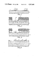
- FIGS. 1-8 sequentially depict the processing steps employed in carrying out the method of the present invention.
- CMOS complementary metal-oxide-semiconductor
- an n-type silicon substrate typically having a resistivity of 0.9 to 1.2 ohms-cm is shown as element 10 over which rests a thin layer of silicon dioxide (SiO 2 ), which can be grown in dry or steam conditions typically to a thickness of approximately 300-500 A.
- SiO 2 silicon dioxide
- a short p-channel transistor with masked channel length of 2.5 ⁇ m can be made without additional channel implantation.
- other n-type silicon bodies can be employed with various resistivities in practicing the present invention.
- a silicon nitride film is deposited preferably within the thickness range of between approximately 1,000-1,500 A in a conventional manner over which is applied photoresist which is exposed and thus hardened in imagewise configuration employing standard photolithographic techniques.
- the nitride and protective photoresist remain as areas 2 and 3 and 4 and 5, hereinafter referred to as "first and second regions", which will be sites for later configured transistors.
- resist 3 and 5 is shown as having been removed to expose nitride areas 2 and 4.
- a field oxide 6 is grown over the entire surface to uniformly grown to a thickness approximately above 2,000 A.
- this oxide serves as a mask against subsequent field implantation.
- the field oxide typically does not grow over nitride and, as such, its cross-sectional profile is typified by that shown in FIG. 2.
- Layer 7 is next applied over field oxide 6 which can be any material which can be selectively etched either with field oxide 6 or individually while leaving the field oxide intact.
- field oxide 6 can be any material which can be selectively etched either with field oxide 6 or individually while leaving the field oxide intact.
- materials such as LPCVD oxide or VAPOX oxide, as well as metal films such as aluminum films, can be employed generally in a thickness range of between approximately 0.5 ⁇ m to 1.0 ⁇ m.
- oxide layer 6 is exposed by applying photoresist 9 over etchable layer 7.
- exposed region 8 is approximately 10 ⁇ m or greater in width and is used for the ion implantation of p-type materials such as boron ions 11. These ions are used to form the p-well region and are generally applied to the surface in doses of approximately 3 ⁇ 10 12 to 1 ⁇ 10 13 ions/cm 2 resulting in a p-well bulk concentration after drive-in of approximately 5 ⁇ 10 15 to 2 ⁇ 10 16 ions/cm 3 .
- oxide 6 and etchable layer 7 are further removed below photoresist 9 to expose areas 12 as depicted in FIG. 3.
- the width of area 12 along silicon body 10 is configured to be equal to approximately the width of the soon to be formed p-well region.
- the width of area 12 should be approximately equal to the depth of the later formed p-well junction divided by ⁇ 2.
- the width of region 12 would be approximately 1.4 to 5.0 ⁇ m.
- p-type impurity 11 When p-type impurity 11 was implanted within region 8, it was done at an energy level high enough so that the impurity penetrated nitride layer 4, but the energy level was not high enough to enable the impurity to penetrate oxide layer 7. Thus, all of the p-type impurity was in an area surrounding nitride layer 4, which is then subjected to a drive-in cycle to implant the impurity such as boron ions to define p-well region 13 which, for purposes of illustration, is formed to a depth of between approximately 2 to 7 ⁇ m.
- etchable layer 7 and photoresist layer 9 can be removed prior to the carrying out of the drive-in cycle, which is preferably performed at temperatures between approximately 1100°-1200° C.
- further implantation is carried out preferably with either boron or BF 2 + ions 14 at an energy low enough to allow implantation at p-well 13, but not in regions covered by either oxide or nitride, shown in FIG. 5 as regions 4, 2 and 6.
- these later applied dopants are employed in the dose range of approximately 2 ⁇ 10 12 to 8 ⁇ 10 12 ions/cm 2 .
- a field implantation has been achieved which is completely self-aligned and defined by the actual boundary established by the p-well lateral diffusion.
- No secondary masks were required to form elaborate high density channel stops, i.e., at densities of approximately 3 ⁇ 10 16 ions/cm 3 , the lateral spacing of p-well 13 being somewhat independent of the depth of the p-well, which is in marked contrast to the processes employed by the prior art.
- the p-well can be doped to increase its field threshold voltage with no additional masking steps other than the single masking step used to form the p-well region itself.
- an opposite impurity type 15 such as phosphorus or arsenic ions are uniformly applied to the surface of silicon substrate 10 at an energy level which is high enough to achieve implantation but low enough so that penetration cannot be carried out through nitride layers 2 and 4.
- ions 15 are implanted within p-well region 13 and n-type region 16 to enhance the p-field threshold voltage even further.
- a second field oxide layer 17 is grown to a thickness of approximately 0.5 to 1.5 ⁇ m by, for example, the conventional steam oxidation process. As noted, the oxide does not grow above nitride layers 2 and 4 which are the sites of the later formed active elements. In progressing to FIG. 8, nitride layers 2 and 4 are removed prior to formation of the active devices.
- the active devices are fabricated by reference to FIG. 8.
- a gate oxide 18 and polycrystalline silicon gate electrode 19 are shown disposed above and between source and drain regions 20 and 21 of the n-channel device in p-well 13.
- the source and drain regions are formed in alignment with gate 19 and field oxide 17.
- gate oxide 22 and polysilicon gate electrode 23 for the p-channel device are shown in alignment with the source and drain regions 24 and 25 which are, in turn, formed in alignment with field oxide 17.
- Leads 27 can then be applied which are isolated by oxide layer 29 and the structure completed by passivation layer 28.
- the ion implantation carried out in conjunction with reference to FIG. 5 is applied uniformly over the surface of the silicon substrate and is thus implanted into the p-well region without any additional masking steps.
- This implantation virtually completely eliminates weak field regions which appear laterally in prior art p-well containing structures. It further eliminates any weak field inversion regions and thus stray leakage channels from polysilicon or metal electrodes placed atop the active areas.
- both the n-channel and p-channel field regions are shown as being self-aligned without using extra masks other than the standard p-well mask shown in FIG. 3.
Landscapes
- Metal-Oxide And Bipolar Metal-Oxide Semiconductor Integrated Circuits (AREA)
Abstract
Description
Claims (13)
Priority Applications (1)
| Application Number | Priority Date | Filing Date | Title |
|---|---|---|---|
| US06/612,927 US4567640A (en) | 1984-05-22 | 1984-05-22 | Method of fabricating high density CMOS devices |
Applications Claiming Priority (1)
| Application Number | Priority Date | Filing Date | Title |
|---|---|---|---|
| US06/612,927 US4567640A (en) | 1984-05-22 | 1984-05-22 | Method of fabricating high density CMOS devices |
Publications (1)
| Publication Number | Publication Date |
|---|---|
| US4567640A true US4567640A (en) | 1986-02-04 |
Family
ID=24455166
Family Applications (1)
| Application Number | Title | Priority Date | Filing Date |
|---|---|---|---|
| US06/612,927 Expired - Lifetime US4567640A (en) | 1984-05-22 | 1984-05-22 | Method of fabricating high density CMOS devices |
Country Status (1)
| Country | Link |
|---|---|
| US (1) | US4567640A (en) |
Cited By (3)
| Publication number | Priority date | Publication date | Assignee | Title |
|---|---|---|---|---|
| US4710265A (en) * | 1985-11-30 | 1987-12-01 | Nippon Gakki Seizo Kabushiki Kaisha | Method of producing semiconductor integrated circuit having parasitic channel stopper region |
| US4713329A (en) * | 1985-07-22 | 1987-12-15 | Data General Corporation | Well mask for CMOS process |
| US4925806A (en) * | 1988-03-17 | 1990-05-15 | Northern Telecom Limited | Method for making a doped well in a semiconductor substrate |
Citations (26)
| Publication number | Priority date | Publication date | Assignee | Title |
|---|---|---|---|---|
| US3983620A (en) * | 1975-05-08 | 1976-10-05 | National Semiconductor Corporation | Self-aligned CMOS process for bulk silicon and insulating substrate device |
| US4013484A (en) * | 1976-02-25 | 1977-03-22 | Intel Corporation | High density CMOS process |
| US4043025A (en) * | 1975-05-08 | 1977-08-23 | National Semiconductor Corporation | Self-aligned CMOS process for bulk silicon and insulating substrate device |
| US4045259A (en) * | 1976-10-26 | 1977-08-30 | Harris Corporation | Process for fabricating diffused complementary field effect transistors |
| US4047284A (en) * | 1975-05-08 | 1977-09-13 | National Semiconductor Corporation | Self-aligned CMOS process for bulk silicon and insulating substrate device |
| US4131907A (en) * | 1977-09-28 | 1978-12-26 | Ouyang Paul H | Short-channel V-groove complementary MOS device |
| US4135955A (en) * | 1977-09-21 | 1979-01-23 | Harris Corporation | Process for fabricating high voltage cmos with self-aligned guard rings utilizing selective diffusion and local oxidation |
| US4143388A (en) * | 1976-05-18 | 1979-03-06 | Matsushita Electric Industrial Co., Ltd. | Mos type semiconductor device |
| US4152717A (en) * | 1975-07-18 | 1979-05-01 | Tokyo Shibaura Electric Co., Ltd. | Complementary MOSFET device |
| US4183134A (en) * | 1977-02-15 | 1980-01-15 | Westinghouse Electric Corp. | High yield processing for silicon-on-sapphire CMOS integrated circuits |
| US4282648A (en) * | 1980-03-24 | 1981-08-11 | Intel Corporation | CMOS process |
| US4295266A (en) * | 1980-06-30 | 1981-10-20 | Rca Corporation | Method of manufacturing bulk CMOS integrated circuits |
| US4306916A (en) * | 1979-09-20 | 1981-12-22 | American Microsystems, Inc. | CMOS P-Well selective implant method |
| US4314857A (en) * | 1979-07-31 | 1982-02-09 | Mitel Corporation | Method of making integrated CMOS and CTD by selective implantation |
| US4335504A (en) * | 1980-09-24 | 1982-06-22 | Rockwell International Corporation | Method of making CMOS devices |
| US4372033A (en) * | 1981-09-08 | 1983-02-08 | Ncr Corporation | Method of making coplanar MOS IC structures |
| US4373253A (en) * | 1981-04-13 | 1983-02-15 | National Semiconductor Corporation | Integrated CMOS process with JFET |
| US4376336A (en) * | 1980-08-12 | 1983-03-15 | Tokyo Shibaura Denki Kabushiki Kaisha | Method for fabricating a semiconductor device |
| US4382827A (en) * | 1981-04-27 | 1983-05-10 | Ncr Corporation | Silicon nitride S/D ion implant mask in CMOS device fabrication |
| US4385947A (en) * | 1981-07-29 | 1983-05-31 | Harris Corporation | Method for fabricating CMOS in P substrate with single guard ring using local oxidation |
| US4391650A (en) * | 1980-12-22 | 1983-07-05 | Ncr Corporation | Method for fabricating improved complementary metal oxide semiconductor devices |
| US4406710A (en) * | 1981-10-15 | 1983-09-27 | Davies Roderick D | Mask-saving technique for forming CMOS source/drain regions |
| US4409726A (en) * | 1982-04-08 | 1983-10-18 | Philip Shiota | Method of making well regions for CMOS devices |
| US4412375A (en) * | 1982-06-10 | 1983-11-01 | Intel Corporation | Method for fabricating CMOS devices with guardband |
| US4420872A (en) * | 1980-12-23 | 1983-12-20 | U.S. Philips Corporation | Method of manufacturing a semiconductor device |
| US4450021A (en) * | 1982-02-22 | 1984-05-22 | American Microsystems, Incorporated | Mask diffusion process for forming Zener diode or complementary field effect transistors |
-
1984
- 1984-05-22 US US06/612,927 patent/US4567640A/en not_active Expired - Lifetime
Patent Citations (26)
| Publication number | Priority date | Publication date | Assignee | Title |
|---|---|---|---|---|
| US3983620A (en) * | 1975-05-08 | 1976-10-05 | National Semiconductor Corporation | Self-aligned CMOS process for bulk silicon and insulating substrate device |
| US4043025A (en) * | 1975-05-08 | 1977-08-23 | National Semiconductor Corporation | Self-aligned CMOS process for bulk silicon and insulating substrate device |
| US4047284A (en) * | 1975-05-08 | 1977-09-13 | National Semiconductor Corporation | Self-aligned CMOS process for bulk silicon and insulating substrate device |
| US4152717A (en) * | 1975-07-18 | 1979-05-01 | Tokyo Shibaura Electric Co., Ltd. | Complementary MOSFET device |
| US4013484A (en) * | 1976-02-25 | 1977-03-22 | Intel Corporation | High density CMOS process |
| US4143388A (en) * | 1976-05-18 | 1979-03-06 | Matsushita Electric Industrial Co., Ltd. | Mos type semiconductor device |
| US4045259A (en) * | 1976-10-26 | 1977-08-30 | Harris Corporation | Process for fabricating diffused complementary field effect transistors |
| US4183134A (en) * | 1977-02-15 | 1980-01-15 | Westinghouse Electric Corp. | High yield processing for silicon-on-sapphire CMOS integrated circuits |
| US4135955A (en) * | 1977-09-21 | 1979-01-23 | Harris Corporation | Process for fabricating high voltage cmos with self-aligned guard rings utilizing selective diffusion and local oxidation |
| US4131907A (en) * | 1977-09-28 | 1978-12-26 | Ouyang Paul H | Short-channel V-groove complementary MOS device |
| US4314857A (en) * | 1979-07-31 | 1982-02-09 | Mitel Corporation | Method of making integrated CMOS and CTD by selective implantation |
| US4306916A (en) * | 1979-09-20 | 1981-12-22 | American Microsystems, Inc. | CMOS P-Well selective implant method |
| US4282648A (en) * | 1980-03-24 | 1981-08-11 | Intel Corporation | CMOS process |
| US4295266A (en) * | 1980-06-30 | 1981-10-20 | Rca Corporation | Method of manufacturing bulk CMOS integrated circuits |
| US4376336A (en) * | 1980-08-12 | 1983-03-15 | Tokyo Shibaura Denki Kabushiki Kaisha | Method for fabricating a semiconductor device |
| US4335504A (en) * | 1980-09-24 | 1982-06-22 | Rockwell International Corporation | Method of making CMOS devices |
| US4391650A (en) * | 1980-12-22 | 1983-07-05 | Ncr Corporation | Method for fabricating improved complementary metal oxide semiconductor devices |
| US4420872A (en) * | 1980-12-23 | 1983-12-20 | U.S. Philips Corporation | Method of manufacturing a semiconductor device |
| US4373253A (en) * | 1981-04-13 | 1983-02-15 | National Semiconductor Corporation | Integrated CMOS process with JFET |
| US4382827A (en) * | 1981-04-27 | 1983-05-10 | Ncr Corporation | Silicon nitride S/D ion implant mask in CMOS device fabrication |
| US4385947A (en) * | 1981-07-29 | 1983-05-31 | Harris Corporation | Method for fabricating CMOS in P substrate with single guard ring using local oxidation |
| US4372033A (en) * | 1981-09-08 | 1983-02-08 | Ncr Corporation | Method of making coplanar MOS IC structures |
| US4406710A (en) * | 1981-10-15 | 1983-09-27 | Davies Roderick D | Mask-saving technique for forming CMOS source/drain regions |
| US4450021A (en) * | 1982-02-22 | 1984-05-22 | American Microsystems, Incorporated | Mask diffusion process for forming Zener diode or complementary field effect transistors |
| US4409726A (en) * | 1982-04-08 | 1983-10-18 | Philip Shiota | Method of making well regions for CMOS devices |
| US4412375A (en) * | 1982-06-10 | 1983-11-01 | Intel Corporation | Method for fabricating CMOS devices with guardband |
Cited By (3)
| Publication number | Priority date | Publication date | Assignee | Title |
|---|---|---|---|---|
| US4713329A (en) * | 1985-07-22 | 1987-12-15 | Data General Corporation | Well mask for CMOS process |
| US4710265A (en) * | 1985-11-30 | 1987-12-01 | Nippon Gakki Seizo Kabushiki Kaisha | Method of producing semiconductor integrated circuit having parasitic channel stopper region |
| US4925806A (en) * | 1988-03-17 | 1990-05-15 | Northern Telecom Limited | Method for making a doped well in a semiconductor substrate |
Similar Documents
| Publication | Publication Date | Title |
|---|---|---|
| US4013484A (en) | High density CMOS process | |
| US6163053A (en) | Semiconductor device having opposite-polarity region under channel | |
| US5880502A (en) | Low and high voltage CMOS devices and process for fabricating same | |
| US4566175A (en) | Method of making insulated gate field effect transistor with a lightly doped drain using oxide sidewall spacer and double implantations | |
| KR930010121B1 (en) | Process for forming high and low voltage CMOS transistors on a single integrated circuit chip | |
| US4342149A (en) | Method of making very short channel length MNOS and MOS devices by double implantation of one conductivity type subsequent to other type implantation | |
| US4745079A (en) | Method for fabricating MOS transistors having gates with different work functions | |
| US4525920A (en) | Method of making CMOS circuits by twin tub process and multiple implantations | |
| US4385947A (en) | Method for fabricating CMOS in P substrate with single guard ring using local oxidation | |
| US4637124A (en) | Process for fabricating semiconductor integrated circuit device | |
| US3898105A (en) | Method for making FET circuits | |
| US4402761A (en) | Method of making self-aligned gate MOS device having small channel lengths | |
| US4562638A (en) | Method for the simultaneous manufacture of fast short channel and voltage-stable MOS transistors in VLSI circuits | |
| US4891326A (en) | Semiconductor device and a process for manufacturing the same | |
| US4135955A (en) | Process for fabricating high voltage cmos with self-aligned guard rings utilizing selective diffusion and local oxidation | |
| EP0218408A2 (en) | Process for forming lightly-doped-grain (LDD) structure in integrated circuits | |
| US5970338A (en) | Method of producing an EEPROM semiconductor structure | |
| GB1603050A (en) | Semiconductor device and a method for making such device | |
| US4713329A (en) | Well mask for CMOS process | |
| US4131907A (en) | Short-channel V-groove complementary MOS device | |
| US4294002A (en) | Making a short-channel FET | |
| US4485390A (en) | Narrow channel FET | |
| JPS55151363A (en) | Mos semiconductor device and fabricating method of the same | |
| EP0091256A2 (en) | CMOS device | |
| US4567640A (en) | Method of fabricating high density CMOS devices |
Legal Events
| Date | Code | Title | Description |
|---|---|---|---|
| AS | Assignment |
Owner name: DATA GENERAL CORPORATION, 4400 COMPUTER DRIVE, WES Free format text: ASSIGNMENT OF ASSIGNORS INTEREST.;ASSIGNORS:FANG, ROBERT C. Y.;WANG, JERRY S. H.;REEL/FRAME:004296/0610 Effective date: 19840507 |
|
| STCF | Information on status: patent grant |
Free format text: PATENTED CASE |
|
| FEPP | Fee payment procedure |
Free format text: PAYOR NUMBER ASSIGNED (ORIGINAL EVENT CODE: ASPN); ENTITY STATUS OF PATENT OWNER: LARGE ENTITY |
|
| FPAY | Fee payment |
Year of fee payment: 4 |
|
| FPAY | Fee payment |
Year of fee payment: 8 |
|
| FPAY | Fee payment |
Year of fee payment: 12 |